Note: Descriptions are shown in the official language in which they were submitted.
CA 02961906 2017-03-20
WO 2016/073145 PCT/US2015/055181
1
METHOD AND APPARATUS INCLUDING A BALANCED DC BUS FOR PROVIDING POWER
IN AN ARC WELDER
RELATED APPLICATIONS
[1] This is a continuation-in-part of, and claims the benefit of the filing
date of,
U.S. Patent Application No. 13839235, filed on March 15, 2013, which claims
priority of
provisional application 61674780, filed 7/23/2012, and this application is a
continuation-in-
part of, and claims the benefit of the filing date of, U.S. Patent Application
No. 14469788,
filed on August 27, 2014.
FIELD OF THE INVENTION
[2] The present disclosure relates generally to the art of welding type
power
supplies. More specifically, it relates to welding type power supplies that
include multiple
power processing circuits, such as an inverter type power supply. It has
features and controls
that allow it to be reconfigured as part of a modular welding type power
supply system.
BACKGROUND OF THE INVENTION
[3] There are many known types of welding-type power supplies. Welding-type
power, as used herein, refers to power suitable for electric arc welding,
plasma arc cutting or
induction heating. Welding type system, as used herein, is a system that can
provide welding
type power, and can include control and power circuitry, wire feeders, and
ancillary
equipment. Welding-type power supply, as used herein, is a power supply that
can provide
welding type power.
[4] Providing welding-type power, and designing systems to provide welding
type
power, provides unique challenges. Welding type systems will often be moved
from one
location to another, and be used with different inputs, such as single or
three phase, or 115V,
230V, 460V, 575V, etc., or 50hz or 60hz signals. Power supplies that are
designed for a
single input cannot provide a consistent output across different input
voltages, and
CA 02961906 2017-03-20
WO 2016/073145 PCT/US2015/055181
2
components in these power supplies that operate safely at a particular input
level can be
damaged when operating at an alternative input level. Also, power supplies for
most fields
are designed for relatively steady loads. Welding, on the other hand, is a
very dynamic
process and numerous variables affect output current and load, such as arc
length, electrode
type, shield type, air currents, dirt on the work piece, puddle size, weld
orientation, operator
technique, and lastly the type of welding process determined to be most
suitable for the
application. These variables constantly change, and lead to a constantly
changing and
unpredictable output current and voltage. Power supplies for many fields are
designed for
low-power outputs. Welding-type power supplies are high power and present many
problems,
such as switching losses, line losses, heat damage, inductive losses, and the
creation of
electromagnetic interference. Accordingly, welding-type power supply designers
face many
unique challenges.
[5] Additionally, welding-type power supplies or systems are often sold for
one or
more particular processes, such as stick, TIG, MIG, pulse, sub-arc, heating,
cutting, and the
maximum output power or current can be anywhere from one hundred or less amps,
to five
hundred or more. The maximum output of a particular welding-type system is
chosen for the
process and/or commercial market for which it is intended. While welding type
power is a
high power level, some welding type systems must provide power and/or output
current than
others. For example, the required output of a 300 amp stick welding system is
different from
the required output of a 600 amp MIG welding system.
[6] Prior art welding type systems have typically been designed for a
particular
output, and the power circuitry, controller, output circuitry, etc., are
designed with the
maximum output power in mind. A 100 amp system might be different from a 200
amp
machine, which is different from a 300 amp machine and so forth. Thus, a
welding type
system is often designed from the ground up. Other times, in an effort to
reduce the attending
engineering costs, a welding-type power supply is scaled up for a higher
output by increasing
switch capacities, or placing switches in parallel. However, there are limits
to this sort of
scaling up, and it gets ever more costly for components to tolerate ever
greater currents. Both
of these approaches in designing new welding type systems required extensive
design,
engineering, and testing, and were thus relatively expensive.
3
[7] USP 6713721, which may be referred to for details, entitled Method of
Designing and
Manufacturing Welding-Type Power Supplies, issued to Albrecht on March 30,
2004, teaches to use
a single power topology with a given output current, and then to place modules
in parallel as needed
to obtain a desired output current. For example, if each module produces 250
amps, and 750 amps is
needed, then three parallel modules are used. While using modules in parallel
as taught in USP
6713721 provides for increased output current, the output voltage for multiple
modules is no higher
than the output voltage for a single module.
[8] One prior art welding type power supply that is well suited for
portability and for receiving
different input voltages is a multi-stage system with a preregulator to
condition the input power and
provide a stable bus, and an output circuit that converts or transforms the
stable bus to a welding-type
output. Examples of such welding-type systems are described in USP 7049546
(Thommes) and USP
6987242 (Geissler), and US Patent Publication 20090230941 (Vogel), all three
of which are owned
by the owner of this disclosure, and may be referred to for details. Millers
welders with the
Autoline feature include some of the features of this prior art.
[9] There are many types of welding type power supplies that can provide a
welding type power
output from an AC or DC source of power. One general category of power supply
is known as a
switched-mode power supply that utilizes power semiconductor switches to chop
a DC source of
power and convert this chopped power to a voltage and/or current suitable for
welding.
[10] One type of switched-mode power supply is commonly known in the welding
industry is an
inverter type power supply. An inverter type power supply chops the source of
DC power and
applies to the primary of a transformer. The frequency of the chopped voltage
is typically much
higher than the AC line frequency (50 t 60Hz), commonly used as a source of
power. Typical
switching frequencies are in the range of 20 KHz to 100 KHz. This higher
frequency allows the
inverter transformer to be much smaller than a comparable line frequency
transformer. The
secondary of the transformer transforms the chopped voltage to a voltage and
current level suitable
for welding. Typically, the secondary of the transformer is connected to a
rectifier and converted to
DC and fed to a smoothing inductor to filter the output. This smoothed output
is then used as the
output of the welding type power supply. For some welding type power sources,
the DC output is
further processed and converted to an AC welding type output such as for AC
GTAW.
CA 2961906 2019-04-30
4
[11] There are many circuit topologies that can be used for an inverter
based welding type power
supply. Amongst these are topologies commonly known as forward circuit, full-
bridge, half-bridge,
flyback, and others. The source of DC power for these types of power supplies
is typically derived
by rectifying a source of AC line power. An inverter type power supply may
also include a pre-
regulator circuit following the rectifier and preceding the inverter circuit.
The pre-regulator circuit
can serve the function of providing a regulated DC bus voltage to the inverter
circuit that may be at a
voltage level different from the raw rectified AC voltage. This pre-regulator
circuit may also include
a power factor control that can be used to improve the power factor of the
current drawn from the AC
line. One prior art welding type power supply that uses PWM control of the
output is described in
US patent 8455794, which may be referred to for further details.
1121 Figure 1 shows a simplified schematic for an inverter based welding
type power supply
consistent with those shown in USPs 7049546 and 6987242. AC line voltage is
rectified, shown with
three phase AC, could alternately be single phase. Typical values for AC line
voltage can range from
115AC or lower to 600 VAC. The inverter power supply may be designed for a
single nominal AC
line voltage or for a range of AC line voltages. The rectifier may include a
filter capacitor, shown as
C3, and provide an output voltage (Vrectified).
[13] A pre-regulator may be included to provide a regulated bus voltage (Vbus)
which may be
regulated to a voltage greater than the peak of the rectified AC line voltage.
The pre-regulator circuit
may also contain a power factor correction circuit or control to improve the
power factor for the
current or power drawn from the AC line. Figure 1 shows a boost converter
circuit arrangement for
the pre-regulator. The switching of power semi-conductor Z3 is controlled by
the gate drive signal
provided by the pre-regulator/inverter control. The switching of Z3 can be
controlled in such a
manner to provide a regulated Vbus as well as perform power factor correction.
CA 2961906 2019-04-30
CA 02961906 2017-03-20
WO 2016/073145 PCT/US2015/055181
[14] The inverter topology shown is a half-bridge circuit with the primary
of the
high frequency inverter transformer, TI, connected between the center point of
capacitors Cl
& C2 and the junction between power semiconductor switches Z1 & Z2. Power
semiconductor switches are switched on and off by a gate drive circuit which
is shown as part
of the inverter control. The switching frequency and ON/OFF ratio (or duty
cycle, D) of the
power semiconductor switches is controlled by the inverter control to provide
a regulated
output voltage and/or current of the welding type power supply. Z1 & Z2
alternately chop the
DC bus voltage and create a high frequency AC voltage on the primary of the
transformer.
For the half-bridge circuit shown the bus voltage is split in half by the two
capacitors, so
effectively when either Z1 or Z2 is switched on, one half of Vbus is applied
across the
primary of the transformer. The transformer transforms the voltage to a level
suitable for
welding. The center tapped secondary of the transformer is connected to a
diode rectifier (D2,
D3) which rectifies the secondary high frequency AC voltage to create a DC
output. The DC
output is filtered by inductor Li to provide a smoothed output current to a
welding arc.
Additional components and circuits not shown in Figure 1 may be included such
as snubbers
and pre-charge circuits, EMI filters, gate drive circuits, control power
supplies and various
other circuits.
[15] A current sensor (CS1) provides a feedback signal indicative of the
output current
(lout). Voltage feedback is also provided to the inverter control circuit,
V_out. The inverter
control may also provide other functions such as monitoring thermal sensors,
controlling
cooling fans, receiving and sending various status and control signals to
other circuits and
controls such as a welding control. The weld controller shown allows the user
to select and
control a welding process, and may provide various signals, indicators,
controls, meters,
computer interfaces, etc. to allow the user to set up and configure the
welding type power
supply as required for a given welding process. The weld controller typically
will provide a
command signal to the inverter control, indicated as I_ref. This command
signal may be an
output current level for the power supply or may be a more complex waveform or
signal
dependant on the particular weld process and user inputs, voltage and current
feedback
signals and other conditions at the welding arc. Voltage feedback, current
feedback, and other
signals may be provided to the weld control.
CA 02961906 2017-03-20
WO 2016/073145 PCT/US2015/055181
6
[16] Welding type power supplies such as shown in Figure 1 are often
designed to
operate from industrial level AC power such as 230, 460 or 575VAC. As such the
bus voltage
Vbus may be greater than 900 Volts. This level of bus voltage may require
power
semiconductor switches (Z1,Z2,Z3) that have voltage ratings on the order of
1200Volts.
Circuits such as snubbers, slow voltage transition (SVT) or other circuits may
be required to
reduce switching losses within the power semiconductors because of the bus
voltage level. In
addition a series arrangement of bulk capacitors (Cl ,C2) may be required to
attain sufficient
voltage rating. These capacitors may not share the voltage perfectly and end
up with a
mismatch voltage level.
[17] Welding type power supplies are often designed with components that
can
handle the full range of input voltage and power and provide a given welding
type power
output. This may not be optimum for certain applications, making the welding
type power
supply more complex or expensive than may be necessary.
[18] It can be desirable to have a welding type power supply that can
handle a
range of inputs such as illustrated above, yet use lower voltage power
semiconductors which
may switch more efficiently and reduce or eliminate the need for snubbers and
other circuits
to reduce switching losses. It can also be desirable to maintain a well
balanced sharing of
voltage for bus capacitors when a series arrangement is used. It can also be
desirable to
provide a welding type power supply that can be readily adapted for different
input voltages
and power levels along with various welding outputs.
[19] Accordingly, a welding-type system having a power topology comprised of a
modular
system, preferably one that can provide a desired output current greater than
the output of any
one module, and/or an output voltage greater than the output voltage of any
one module is
desired. Preferably, the system maintains the advantages of prior art
portable, universal input
systems, but also avoids some of the deficiencies of the prior art is desired.
SUMMARY OF THE PRESENT INVENTION
[20] According to a first aspect of the disclosure a welding-type power
supply
includes a controller, a preregulator, a preregulator bus, and an output
converter. The
CA 02961906 2017-03-20
WO 2016/073145 PCT/US2015/055181
7
controller has a preregulator control output and an output converter control
output. The
preregulator receives a range of inputs voltages as a power input, and
receives the
preregulator control output as a control input, and provides a preregulator
power output
signal. The preregulator includes a plurality of stacked boost circuits. The
preregulator bus
receives the preregulator output signal. The output converter receives the
preregulator bus as
a power signal and receives the output converter control output as a control
input. The output
converter provides a welding type power output, and includes at least one
stacked inverter
circuit.
[21] According to a second aspect of the disclosure a welding-type power
supply
includes a controller, a preregulator, a preregulator bus, and an output
converter. The
controller has a preregulator control output and an output converter control
output. The
preregulator receives a range of inputs voltages as a power input, and
receives the
preregulator control output as a control input, and provides a preregulator
power output
signal. The preregulator includes a stacked boost circuit. The preregulator
bus receives the
preregulator output signal. The output converter receives the preregulator bus
as a power
signal and receives the output converter control output as a control input.
The output
converter provides a welding type power output, and includes at least one
stacked inverter
circuit.
[22] The controller includes a bus voltage balancing module in another
embodiment. The bus voltage balancing module includes one or both of an
integrator and an
accumulator in various embodiments, and/or receives feedback from the pre-
regulator and
output converter in various embodiments.
[23] According to a third of the disclosure a welding-type power supply
includes a
controller, a preregulator, a preregulator bus, and an output converter. The
controller has a
preregulator control output and an output converter control output. The
controller includes a
bus voltage balancing module, and the preregulator control output is
responsive to the bus
voltage balancing module. The preregulator receives a range of inputs voltages
as a power
input, and receives the preregulator control output as a control input, and
provides a
preregulator power output signal. The preregulator provides a preregulator
output signal and
provides feedback to the bus voltage balancing module. The preregulator
includes at least one
CA 02961906 2017-03-20
WO 2016/073145 PCT/US2015/055181
8
stacked boost circuit. The preregulator bus receives the preregulator output
signal. The output
converter receives the preregulator bus as a power signal and receives the
output converter
control output as a control input. The output converter provides a welding
type power output,
and includes at least one stacked inverter circuit.
[24] The preregulator bus is voltage regulated in one embodiment.
[25] The output converter includes a dual stacked inverter in another
embodiment.
[26] The plurality of stacked boost circuits is a dual stacked boost
circuit, a triple
stacked boost circuit, or more than three stacked boost circuits in various
embodiments.
[27] The controller includes a current balance module and/or an output
converter
flux balancing module in various embodiments.
[28] The controller includes a start up module and/or a power down module
in
other embodiments.
[29] The controller includes a power circuit configuration detection
module, and
one or both of the preregulator control output and the output converter
control output are
responsive to the power circuit configuration detection module in another
embodiment.
[30] The welding-type power also has a user-notification module responsive
to the
power circuit configuration detection module and an auxiliary power circuit
detection module
in another embodiment.
[31] The welding-type power supply also includes a synthetic auxiliary ac
power
circuit having an ac adjustable frequency auxiliary power output and/or a
variable speed
cooling fan receives auxiliary power output and blows air toward at least part
of the
preregulator and the output converter in another embodiment.
[32] The output converter includes a stacked full bridge inverter in
another
embodiment.
CA 02961906 2017-03-20
WO 2016/073145 PCT/US2015/055181
9
[33] According to another aspect of the disclosure a welding-type power
supply
includes a bus (which can but need not be preregulated), an output converter,
and a controller.
The output converter receives the bus and provides a welding type power
output. the bus also
has a control input, and switches in the output converter are controlled by
the control input.
The controller receives bus feedback signal indicative of a plurality of bus
voltages. The
controller also has a converter control output connected to the control input.
A bus voltage
balancing module in the converter includes a scaled correction module
responsive to the bus
feedback signal, and the converter control output is responsive to the bus
voltage balancing
module.
[34] According to another aspect of the disclosure a method of providing
welding-
type power includes providing a bus (which can but need not be preregulated)
and converting
the bus using a switched converter to a welding type power output. The
converting is
controlled in response to bus feedback indicative of a plurality of bus
voltages, by adjusting
pulse widths of switches in the converter in proportion, over a range, to a
difference between
the plurality of bus voltages to balance the bus.
[35] According to another aspect of the disclosure a welding-type power
supply
includes a bus (which can but need not be preregulated), an output converter,
and a controller.
The output converter receives the bus and provides a welding type power output
in response
to a control input because switches in the output converter are controlled by
the control input.
The controller receives load feedback indicative of a load output, and
provides a converter
control output connected to the control input. The controller has a bus
voltage balancing
module that includes a load proportional gain module responsive to the load.
[36] According to another aspect of the disclosure a method of providing
welding-
type power includes providing a split preregulated bus having first and second
bus voltages,
and converting the preregulated bus using a stacked inverter to a welding type
power output.
A first inverter receives the first bus voltage and a second inverter receives
the second bus
voltage. The converting is controlled in response to bus feedback indicative
of the first and
second of bus voltages by adjusting pulse widths of switches in the converter
in proportion,
over a range, to a difference between the plurality of bus voltages to balance
the preregulated
10
bus. Load feedback indicative of a load output is received, and pulse widths
of switches are adjusted in
the converter in inverse proportion, over a range, to the load feedback.
[37] The controller also receives load feedback indicative of a load
output, and the bus voltage
balancing module includes a load proportional gain module responsive to the
load feedback in one
embodiment.
[38] The controller further receives feedback indicative of an open circuit
voltage (OCV) or load
condition, and the bus voltage balancing module includes a duty cycle limiting
module responsive to the
open circuit voltage (OCV) feedback in another embodiment.
[39] A preregulator provides power to the preregulator bus in one
embodiment.
[40] The bus is a split bus with a first bus voltage and a second bus
voltage and the bus feedback
signal is responsive to a difference between the first and second bus voltages
exceeding a threshold in
another embodiment.
[41] The switched converter is a stacked inverter having at least two
inverter and the preregulated
bus is a split bus having two bus voltages, each feeding an inverter and the
plurality of bus voltages are
the two bus voltages, each feeding an inverter and the plurality of bus
voltages are the two bus voltages,
and the adjusting includes providing a greater pulse width a first one of the
two inverters, wherein the
first one of the two inverters receives a bus voltage that is greater than a
second bus voltage received by
a second inverter, wherein the pulse width is greater in proportion, over a
range, to a difference
between the plurality of bus voltages, thereby balancing the preregulated bus,
in various embodiments.
[42] Load feedback indicative of a load output is received, and the pulse
widths are adjusted in
inverse proportion, over a range, to the load feedback, in another embodiment.
[43] OCV feedback indicative of an OCV or load condition is received, and
the duty cycle of the
switched converter is limited in response to the OCV feedback in one
embodiment.
CA 2961906 2018-06-20
CA 02961906 2017-03-20
WO 2016/073145 PCT/US2015/055181
11
[44] The controller receives a bus feedback signal indicative of a
plurality of bus
voltages, and the bus voltage balancing module includes a scaled correction
module
responsive to the bus feedback signal, and the converter control output is
responsive to the
bus voltage balancing module, in various embodiments.
BRIEF DESCRIPTION OF THE DRAWINGS
[45] Figure 1 is schematic for a prior art inverter based welding type
power supply;
[46] Figure 2 is a dual stacked boost pre-regulator power circuit in
accordance with
the preferred embodiment;
[47] Figure 3 is a single stacked boost pre-regulator power circuit in
accordance
with the preferred embodiment;
[48] Figure 4 is a dual stacked full bridge inverter output converter in
accordance
with the preferred embodiment;
[49] Figure 5 is a stacked full bridge inverter output converter in accordance
with the
preferred embodiment;
[50] Figure 6 is a block diagram of a welding-type power supply in
accordance
with the preferred embodiment;
[51] Figure 7 is a controller for a pre-regulator in accordance with the
preferred
embodiment;
[52] Figure 8 is a controller for a stacked boost pre-regulator circuit in
accordance
with the preferred embodiment;
[53] Figure 9 is a control loop for a dual stacked boost pre-regulator
circuit in
accordance with the preferred embodiment;
CA 02961906 2017-03-20
WO 2016/073145
PCT/US2015/055181
12
[54] Figure 10 is a controller for an inverter-based output converter in
accordance
with the preferred embodiment;
[55] Figure 11 is a controller for an inverter-based output converter in
accordance
with the preferred embodiment;
[56] Figure 12 shows four PWM signals for the inverter-based output
converter in
accordance with the preferred embodiment; and
[57] Figure 13 is a control loop for an inverter based output converter in
accordance with the preferred embodiment;
[58] Before explaining at least one embodiment of the method and system in
detail
it is to be understood that the disclosure is not limited in its application
to the details of
construction and the arrangement of the components set forth in the following
description or
illustrated in the drawings. The method and system is capable of other
embodiments or of
being practiced or carried out in various ways. Also, it is to be understood
that the
phraseology and terminology employed herein is for the purpose of description
and should
not be regarded as limiting. Like reference numerals are used to indicate like
components.
DETAILED DESCRIPTION OF THE PREFERRED EMBODIMENTS
[59] While the method and system will be illustrated with reference to
particular
circuits and topologies it should be understood at the outset that the method
and system can
be implemented with other circuits and topologies.
[60] Generally, the method and system include a welding type power supply
with a
dual stacked boost pre-regulator circuit and a dual stacked full bridge
inverter circuit output
converter. Stacked boost circuit, as used herein, is a boost circuit including
two switches, two
diodes, and two capacitors in a series arrangement, wherein the collector of
one switch is
connected to the emitter of the other switch, and each switch has an inductor
associated
therewith. Each switch is clamped to its associated bus capacitor by the
series arrangement
with the diodes. A single stacked boost may have one inductor connected to
either the upper
CA 02961906 2017-03-20
WO 2016/073145 PCT/US2015/055181
13
or lower switch. A dual boost preferably has an inductor with each switch so
that the current
can be balanced between the two upper branches, and likewise for the two lower
branches.
Stacked boost circuit can have groups of parallel switches. If a MOSFET
switches are used,
they are connected drain to source, and if other switches are used they are
connected in like
manner. Fig. 3 shows a stacked boost circuit. Stacked inverter circuit, as
used herein, is two
inverter circuits with the primary side switches connected in series. A single
stacked inverter
circuit is an arrangement of at least one switch connected to a lower bus and
at least one
switch connected to an upper bus driving at single transformer.
[61] One configuration of the welding type power supply consists of a
single
stacked boost pre-regulator circuit to provide a lower power configuration for
the pre-
regulator circuit. Another configuration of the welding type power supply
consists of a single
stacked full bridge inverter circuit to provide a lower power configuration
for the inverter
power circuit. A controller is provided to control the operation of the pre-
regulator and output
circuits. Controller, as used herein, is the digital and/or analog circuitry
and/or
logic/instructions that cooperate to provide control signals to one or more
circuits. A
controller can be located on a single board, or distributed across multiple
locations. Dual
stacked boost circuit, as used herein, is two stacked boost circuits connected
in parallel, with
a common output bus, also fed from a common input rectifier. Alternatives
include two
rectifiers fed from a common AC source, and/or two separate output busses.
Output
converter, as used herein, is power circuitry that receives an intermediate
signal such as a bus
and provides an output power signal. Output converter control output, as used
herein, is a
control output used to control one or more switches in an output converter,
and can be
comprised of multiple control signals. Preregulator, as used herein, is a
power circuit that
receives input power one form, and provides it in another form to another
power processing
circuit. Preregulator bus, as used herein, is the bus that is the output of a
preregulator.
Preregulator control output, as used herein, is a control output used to
control one or more
switches in an preregulator, and can be comprised of multiple control signals.
Preregulator
output signal, as used herein, is the power output of a preregulator.
[62] The controller provides various control algorithms and features.
Preferably, it
includes a plug and play module that can detect the power circuit
configuration and adapt or
modify the control as required, provide status information to the user as to
the detected
CA 02961906 2017-03-20
WO 2016/073145 PCT/US2015/055181
14
configuration and possible operation outside of the intended parameters,
detect optional
power supplies and adapt or modify a control based on the presence of these
supplies
(example: 115VAC aux. power circuit, wire feeder power supply, etc.). Power
circuit
configuration detection module, as used herein, is a control module that
detects the
configuration of a power supply, such as whether a single or dual stacked
boost circuit is
being used. Module, as used herein, is software and/or hardware that
cooperates to perform
one or more tasks, and can include digital commands, control circuitry, power
circuitry,
networking hardware, etc.
[63] Also, the system preferably includes a module for actively balancing a
bus
voltage shared between two or more series capacitors, such as an accumulator
or integrator
function, to accumulate a bus voltage difference, with coordination of bus
balancing between
pre-regulator and inverter or other circuits.
[64] The system preferably includes a module for actively balancing current
flow
for a dual boost configuration and/or a module for coordinating and
controlling start up and
shut down of aux. power supplies, and/or active flux balancing for the
inverter circuit to
reduce the likelihood of transformer saturation, and/or a module for providing
variable speed
fan for cooling, and/or a module for providing various self checks to assure
proper operation
of the pre-regulator and inverter circuits.
[65] A dual stacked boost pre-regulator power circuit is illustrated in
Figure 2. The
output of the pre-regulator circuit shown is a regulated bus voltage indicated
as Vbus. The
bus voltage is shared approximately equally between two series capacitors Cl
and C2.
Vbus_top & Vbus_bottom represent the two capacitor voltages. Capacitors Cl and
C2 may
each be comprised of a single capacitor or multiple capacitors forming a
capacitor bank. The
input to the pre-regulator circuit is provided by a rectifier that converts AC
line voltage to a
rectified DC voltage. The rectifier may be supplied with a range of line
voltages (ex.
230VAC, 460 VAC, 575 VAC) and operate on either single or three phase. Range
of inputs
voltages, as used herein, is a range spanning at least two utility voltages.
[66] The pre-regulator circuit may be designed to operate over a continuous
span of
input voltage and provide an output bus voltage that is regulated at an
approximately constant
CA 02961906 2017-03-20
WO 2016/073145 PCT/US2015/055181
voltage that is greater than the highest rectified voltage (ex. 920VDC).
Alternately, the pre-
regulator may provide a bus voltage that is at a level such that at some AC
line voltages the
pre-regulator shuts down and passes the rectified line voltage without further
boosting (ex.
may stop boosting when line voltage reaches 575VAC + 15%). Also, the pre-
regulator may
be provided with any source of DC voltage such as from a battery or generator.
In some cases
AC line voltage may be provided by a generator, alternator or utility power.
The preregulator
preferably provides a voltage regulated bus. Voltage regulated bus, as used
herein, is a bus
regulated to a desired voltage or voltage waveform.
[67] The pre-regulator circuit shown in Figure 2 is comprised of two boost
circuits
with series connected switches (dual stacked boost). The first boost circuit
is comprised of
series switches Z4,Z5, diodes D5,D6, inductors L7,L8 and current sensor CS7.
Alternately an
additional current sensor may be provided in series with inductor L8. The
magnitude of the
current flowing in L8 may be calculated or inferred from the current flowing
in the other
inductors (L7,L9,L10) and as such this additional current sensor may not be
required.
Alternatives provide for using two, three, four or more stacked boost circuits
in parallel.
Plurality of stacked boost circuits, as used herein, is two or more stacked
boost circuits
arranged in parallel.
[68] Switches Z4 & Z5 are controlled and switched ON & OFF at a switching
frequency (10Khz to 20Khz or more, e.g.) with the ON time controlled or
modulated by a
control circuit as required to regulate the bus voltage while also controlling
and regulating the
current flowing in the inductors L7 & L8. Two pulse width modulation signals
are provided
to control Z4 & Z5 independently (PWM1 & PWM2). In general, control of these
switches is
similar to the well known boost circuit shown in Figure 1, other than it may
be desirable to
phase stagger the two PWM signals or interleave the switching signals.
Interleaving has a
benefit of effectively doubling the ripple current frequency present in the
inductors L7 & L8,
which may allow reduction of the switching frequency of Z4 & Z5, reduce the
filtering
requirements and relative size of L7 & L8, along with other benefits. Other
modifications of
PVVM1 and/or PVVM 2 may be implemented as described in more detail below to
provide bus
voltage balancing and current balancing with a second boost circuit. The
series arrangement
of Z4 & Z5 along with diodes D5 & D6 result in a voltage impressed across
these devices
CA 02961906 2017-03-20
WO 2016/073145 PCT/US2015/055181
16
that is approximately one half Vbus. This may allow more efficient devices to
be used and
reduce or eliminate the need for snubbers, SVT or other circuits to reduce
switching losses.
[69] A second boost circuit is comprised of switches Z6,Z7 diodes D7,D8,
inductors L9,L10 and current sensors CS9,CS10. The second boost output is
connected in
common with the first boost circuit to Vbus. The input is provided from a
common rectifier.
Alternately the second boost circuit may receive its input from a separate
rectifier or other
source of DC power. Switches Z6 & Z7 are controlled by two additional
independent PWM
signals (PWM3, PWM4). These two PWM signals may be similar to the two PWM
signals
provided to the first boost circuit. PWM3 & PWM4 may be interleaved in a
similar fashion as
PWM1 & PWM2. Operation of the second boost circuit is similar to operation of
the first
boost circuit. A more detailed description of the derivation and control of
the four PWM
signals is provided below. The dual boost circuit provides additional power
flow through the
pre-regulator by sharing the current flowing into Vbus, when compared to a
single boost
circuit.
[70] A single stacked boost circuit arrangement for the pre-regulator is
shown in
Figure 3. The description and operation is similar to the description given
above for the first
boost circuit as part of the dual boost arrangement. The control signals PWM1
& PWM2 are
similar and may be interleaved as described above. Modification of PWM1 & PWM2
may be
implemented to achieve bus voltage balancing. Modification of PWM1 & PWM2 for
current
balancing with a second boost however would not be required because there is
no second
boost circuit present. The control algorithm or circuit may be modified to
eliminate the
current balancing modification. As such it may be beneficial and desirable for
a control to
detect the configuration of the pre-regulator circuit (single boost, dual
boost) so that control
modifications may be automatically implemented. In general this arrangement of
single boost
compared to dual boost may reduce the total output boost current flowing into
the DC bus
such that this arrangement is suitable for a lower power welding power supply,
or a welding
power supply that can only operated from a reduced range of input voltages
(ex. 400-
600 VAC, vs. 230-600VAC for a dual boost). This may allow a circuit with
reduced
complexity and cost for some applications that don't require a full range of
input voltages for
example. It may also be desirable to detect the pre-regulator arrangement
(single boost, dual
boost) and provide feedback to the user via an indicator, user interface, or
other means as to
CA 02961906 2017-03-20
WO 2016/073145 PCT/US2015/055181
17
the arrangement and the capability of this arrangement. For example a customer
with a single
boost arrangement may be alerted to an incorrect line voltage if the welding
type power
supply is connected to 230VAC, and the single boost range is intended to be
400-600VAC. It
may therefore be desirable to detect the pre-regulator configuration to allow
various
configurations of welding type power supplies to be manufactured, to allow
modifications in
the field, retrofit, etc. and provide a control that can adapt and provide the
necessary PWM
control signals, as well as provide information to a user based on the
detected configuration.
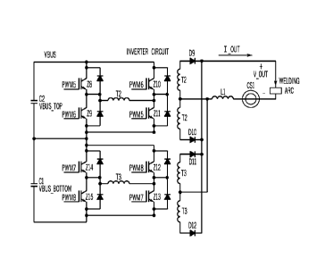
[71] A dual stacked full bridge inverter circuit is shown in Figure 4.
Switches
Z8,Z9,Z10,Z11 transformer T2 and diodes D9,D10 form the basic power circuit
for a first
inverter circuit. Switches Z12,Z13,Z14,Z15 transformer T3 and diodes Dl 1,D12
form a
second inverter circuit. These two circuits are arranged in a series
arrangement on the input or
primary side with each connected across one half of the bus voltage (Vbus_top,
Vbus_bottom). The output or secondary side is arranged in a parallel
arrangement such that
D9,D10 along with T2 share the output current with D11,D12 and T3. The
switches are
switched ON & OFF at a switching frequency (ex. 20Khz to 100Khz) with a pulse
width or
duty cycle that is modulated to control and regulate the output current and/or
voltage as
required to provide a welding type output. These pulse width modulation
signals are indicated
as PWM5, PWM6, PWM7 & PWM8. The basic operation of a full bridge circuit is
well
known and will not be described further other than specific details as it
relates to the control
of the PWM signals. Dual stacked inverter, as used herein, is two stacked
inverters connected
in to have their outputs in parallel. Alternatives provide for a series
connection, which will
result in a higher output voltage. The preferred embodiment has, on the input
side, for a
single inverter with there are 4 switches in series across the two series bus
voltages with a
single transformer. For a dual inverter, 4 switches arranged in a full bridge
driving the
primary of one transformer connected across each bus voltage with the two bus
voltages in
series.
[72] As with the stacked boost circuit, the stacked full bridge arrangement
may
allow the use of lower voltage switches as the primary of each inverter
circuit operates from
one half of the total bus voltage. In addition the stacked arrangement shown
in Figure 4 has
some benefit in that there is an inherent means to split and share the current
on the secondary
and naturally force an approximate balancing of the two bus voltages on the
primary
CA 02961906 2017-03-20
WO 2016/073145 PCT/US2015/055181
18
(VBus_top & Vbus_bottom). For example if the top bus voltage is higher than
the bottom bus
voltage then the secondary voltage of T2 will be higher than the secondary
voltage of T3 and
therefore T2 will take a greater proportion of the output current. This
additional current
reflected to the primary of T2 means that the total power drawn from the top
bus voltage will
be greater than the power drawn by the lower inverter circuit on the bottom
bus. This greater
power will naturally decrease the top bus voltage relative to the total bus
voltage until an
equilibrium point is reached. Thus there is passive balancing or sharing.
Active balancing or
sharing may be desired for certain dynamic or static load conditions such as
for very small
PWM values, such as during a short circuit condition on the output of the
welding type power
supply. Active balancing of the top and bottom bus voltages may be performed
independently
or in conjunction with a voltage balancing means implemented in the control
for a single or
dual stacked boost pre-regulator.
[73] The inherent balancing of the series bus voltages, and sharing of
output
current may perform optimally with a small mismatch in the top and bottom bus
voltages (ex.
2 to 3 volts difference), as naturally arrived at by the tolerances of the
various circuit
components within the inverter circuit, switching characteristics, etc. As
such it may be
desirable to disable active DC bus balancing within the pre-regulator circuit
once the bus
voltage difference falls below a limit (ex. within 5 Volts differential).
[74] In some arrangements of a welding, cutting or heating power supply the
secondary diodes D9, D10, Dll & D12 may be eliminated and the high frequency
AC of T2
& T3 used directly. Other arrangements may include further processing of the
output power
through an AC inverter circuit to provide an AC output power with a frequency
that may be
independent of the inverter switching frequency and independent of the AC line
frequency.
Any number of other additional circuits and controls may be provided as
required within a
welding type system such as thermal sensors, fan control, user interfaces,
weld process
controls, data storage, wire feeders, aux. power supplies, etc.
[75] A stacked full bridge inverter circuit is shown in Figure 5. The basic
inverter
circuit is comprised of switches Z8,Z9,Z14 & Z15 along with transformer T2,
blocking
capacitor C4 and diodes D9,D10. Switches Z8,Z9,Z14 & Z15 are controlled by PWM
signals
PWM5, PWM6, PWM7 & PWM8. In this arrangement switches Z8 & Z15 are switched
CA 02961906 2017-03-20
WO 2016/073145 PCT/US2015/055181
19
more or less together and switches Z9 & Z14 are switched ON and OFF together.
Capacitor
C4 maintains a DC offset voltage approximately equal to one half Vbus. In
general, operation
of this arrangement of full bridge circuit is similar to the operation of one
of the two full
bridge inverter circuits shown in Figure 4, with the main difference being
that when switches
Z9 & Z14 are ON, the voltage across primary of T2 and thus the output power,
is supplied by
the voltage stored on blocking capacitor C4.
[76] A basic system block diagram of the described welding type power
supply is
shown in Figure 6. AC line voltage is supplied to a rectifier circuit followed
by a pre-
regulator circuit. A regulated bus voltage (Vbus) is provided by the pre-
regulator to an
inverter circuit, which in turn provides a welding type power output. An aux.
power circuit
may also be powered from the Vbus signal and provide an aux. power circuit.
For example
the aux. power circuit may provide 115VAC in the form of a rectangular
waveform or a sine
waveform or other suitable waveform. The aux. power circuit may be used in a
welding type
system or cell to power various hand tools, grinders, fans, lights or other
ancillary equipment
that may be found in a weld cell. The aux. power circuit may or may not be
present in some
welding type power supplies. A wire feeder power circuit may also be powered
from the
Vbus signal and provide an output power signal for driving a wire feeder as
part of a welding
system. The wire feeder power output may be a DC signal such as 42VDC, or may
be an AC
signal in other systems. Again the wire feeder power circuit may or may not be
present in
some welding type power supplies depending on the particular configuration.
Other similar
power circuit such as for powering a water cooler, heater, etc. may be
provided in a similar
fashion.
[77] A control may receive input signals and/or provide various control
signals to
control the pre-regulator circuit, inverter circuit and any additional power
circuits as shown in
Figure 6. These signals may include current and voltage feedback signals, PWM
signals,
enable and status signals, analog feedback signals, etc. In other words all of
the necessary
signals as required to monitor and control the power circuits. The control may
also interface
to additional controls and/or circuits such as a weld control, user interface,
etc. as required for
proper operation of the welding type power supply within a welding operation.
The control
may be implemented using control circuits, microprocessors and memory devices,
software
algorithms, or various combinations.
CA 02961906 2017-03-20
WO 2016/073145 PCT/US2015/055181
[78] A pre-regulator control block diagram is shown in Figure 7. Each of
the four
switch circuits (Z4, Z5, Z6, & Z7) are provided with a PWM control signal
generated by the
pre-regulator control, and a detect signal provided to the pre-regulator
control to allow for the
control to detect the presence or lack of presence of the switch circuits.
Each switch circuit
may contain a power semiconductor such as an IGBT, gate drive circuit, thermal
feedback, or
other circuits. The detect signal may be an analog feedback signal or a logic
signal that can be
read or detected by the pre-regulator control to sense the presence of each
particular switch
circuit. As described above the pre-regulator control may alter a control
sequence or
algorithm based on the presence or lack of presence of one or more of the
switch circuits. For
example if the control detects the presence of four switch circuits then a
current balancing
control may be implemented to balance the current flowing in the four
inductors shown in
Figure 2. Interface signals may be provide to a user interface or other
control to indicate the
configuration of the welding type power supply. The switch detect signals may
also be used
to detect and indicate an abnormal situation or possible welding type power
supply fault. For
example if the pre-regulator control detects the presence of 3 of the 4 switch
circuits, this
may be indicated as a fault to the user, and an indication provided as to
which switch was not
detected as an aid for servicing the welding type power supply.
[79] Likewise the three current sensors may be connected to the control as
shown
to provide a current feedback signal indicative of the current flowing in
three of the inductors
shown in Figure 2. The current sensors may also provide a detect signal to the
control, so that
the presence or lack of presence of the current sensors can be detected. In a
pre-regulator
circuit within a welding type power supply it is often desirable to control
the pre-regulator
current in some fashion, to limit the current, to shape the current waveform
to improve the
power factor, to limit the input power or output power from the pre-regulator
circuit, etc.
Utilization of the current detect signal to modify the control or disable
operation if the current
sensor is not detected can help assure proper operation, and/or assist with
servicing of the
welding type power supply. Alternately the presence of the current sensors may
be detected
by looking for a certain threshold of current feedback during operation or
start up of the pre-
regulator circuit. For example a start up sequence may operate the boost pre-
regulator circuit
for a certain time period with a small PWM duty cycle value, such that the
current cannot
climb too rapidly beyond a certain limit, yet allow detection that the sensor
is providing a
CA 02961906 2017-03-20
WO 2016/073145 PCT/US2015/055181
21
feedback signal. Alternately the expected current feedback signal may be
calculated based on
the input rectified voltage supplied to the pre-regulator circuit, the output
bus voltage, the
switch PWM duty cycle values and the inductor values, and this value compared
to the actual
current sensor feedback signals to determine proper operation of the current
sensors.
Additional signals not shown may be provided to the current sensor circuit
such as power
supplies, or other signals required for proper operation.
[80] The pre-regulator control may also be supplied with other signals such
as a
feedback signal indicative of the rectified voltage (V_RECTIFIED_FEEDBACK) and
bus
voltage feedback signals (VBUS_TOP_FEEDBACK, VBUS_BOTTOM_FEEDBACK).
These signals may be used to regulate the bus voltage, implement DC bus
balancing between
top and bottom bus voltages, detect a bus voltage unbalance and take some
action to correct
or disable operation, verify proper input voltage based on a detected pre-
regulator
configuration, or other features and functions. The bus balancing is
accomplished by a bus
voltage balancing module that receives the bus voltage feedback signals, and
causes the
switches to operate in such a way as to bring them closer together. Bus
voltage balancing
module, as used herein, is a control module that controls switching signals so
as to balance a
bus voltage across multiple capacitors.
[81] Various interface signals may be provided to the inverter control,
aux. power
circuit, wire feeder power circuit, pre-charge circuit, and other circuits
within a welding type
system. These interface signals may be provided as outputs by the pre-
regulator control or as
inputs to the pre-regulator control. These interface signals allow for
detection of the presence
of certain circuits such as an aux. power circuit for example and then to take
some action
based on the presence or lack of presence of certain circuits. For example if
an aux. power
circuit is detected as present, then a power up routine for the aux. power
circuit may be
activated as part of the overall power up routine of the welding type power
supply. The aux.
power circuit may be enabled for example only after the pre-regulator has
established Vbus at
its nominal regulated value and determined that it is ok to enable the aux.
power circuit. After
a certain power up time the pre-regulator control may then verify operation of
the aux. power
circuit, and either continue operation or disable operation depending on a
detected status of
the aux. power circuit. This status and operational information may be
communicated to a
user via a user interface.
CA 02961906 2017-03-20
WO 2016/073145 PCT/US2015/055181
22
[82] It may be desirable to limit the total input power or current to the
welding type
power supply in some situations. As such it may be desirable to reduce or
limit the maximum
welding type output power if an aux. power circuit is present. For example if
an aux. power
circuit that can provide up to 2kw of output power is detected as part of the
configuration of
the welding type power supply it may be desirable in some situations to reduce
the maximum
welding output power by 2kw or some amount such that the input power does not
exceed an
upper limit. In addition it may be desirable to modify the control of a
cooling fan based on
detecting the presence of an aux. power supply configuration, or based on an
output power
level of an aux. power supply. This may allow for adequate cooling of aux.
power supply
components during periods when welding power output is at a reduced limit. The
aux. power
circuit is detected in the manner described above for detecting other circuits
using an
auxiliary power circuit detection module. Auxiliary power circuit detection
module, as used
herein, is a control module that detects the presence of, or use of, an aux.
power circuit.
[83] The detection modules can provide configurations to a user-
notification
module, which can notify the user of the configuration, or only notify the
user when there is
an error detected. User-notification module, as used herein, is a control
module that acts to
notify the user of a condition or parameter.
[84] A pre-charge circuit interface may also be provided to allow for the
bus
capacitors to be soft charged or pre-charged prior to operation of the boost
circuit. A relay or
AC line contactor, or other means as is well known may be used as part of a
pre-charge
circuit. The interface signals may contain additional information beyond
detect, enable and
status. For example DC bus voltage signals or information may be provided to
the inverter
control, such that the inverter control may take some action to work in
conjunction with the
pre-regulator control to force a DC bus balance. Any number of other signals
may pass back
and forth between these and other parts of the welding type power supply.
These signals may
be in the form of hardware connections, variables in software, serial
communication, or any
other suitable form.
[85] An example control circuit for a stacked boost pre-regulator circuit
that can
accommodate a single or dual boost arrangement is shown in Figure 8. Circuit
Al is a bus
voltage regulator circuit that provides an output signal to a boost current
regulator circuit.
CA 02961906 2017-03-20
WO 2016/073145 PCT/US2015/055181
23
The output of the bus voltage regulator circuit serves the purpose of
regulating the total bus
voltage to a fixed value (REF), based on feedback signals (VBUS_TOP &
VBUS_BOT). For
some welding type power supplies that require a range of dynamic welding
processes such as
pulse welding it may be desirable to tune the compensation network of the bus
voltage
regulator so that the power flow out of the pre-regulator tends to be more
responsive to the
average welding power requirement and not the dynamic nature of the welding
process. This
may require a compensation network that provides a relatively slow response
(ex. 50 to
100mSec).
[86] Circuit A2 is a boost current regulator circuit that serves the
purpose of
regulating the boost current based on a current feedback signal (CS7). The
output of the
current regulator (I_ERROR) is read as an analog input by a microprocessor and
is used as
one input to determine a PWM duty cycle for the four boost switches (PWM1 ¨
PWM4). For
example PWM1 ¨ PWM4 may be identical initially based on the value of I_ERROR.
[87] Additional analog and digital inputs are provided to the
microprocessor. These
include analog current sensors signals (CS7, CS9 & CS10) that provide feedback
information
proportional to the current flowing in the inductors shown in Figure 2. Analog
bus voltage
feedback signals (VBUS_TOP, VBUS_BOT) are also read by the microprocessor and
may be
used as another input to modify a PWM duty cycle (PWM1 ¨ PWM4) to actively
balance the
two DC bus voltages. A feedback signal representative of the rectified voltage
provided to the
pre-regulator circuit by the input rectifier (V RECTIFIED) may also be
provided. This
feedback signal may be used in various ways such as for detecting an input
voltage that is too
high or too low for a particular pre-regulator configuration, detecting single
phase power, etc.
In some cases the rectified voltage feedback may be used to modify the PWM
values such
that the input current is shaped and aligned with the input AC line voltage to
further improve
power factor.
[88] Z4-Z7 detect signals are provided to the microprocessor and may be
used to
determine the boost configuration or arrangement (single or dual), and also
detect an
abnormal condition. Certain control and status information is communicated
with an inverter
control via a serial communication circuit. Additional signals may be provided
that are not
shown such as rectified voltage feedback, thermal sensors, etc. A circuit may
alternately be
CA 02961906 2017-03-20
WO 2016/073145 PCT/US2015/055181
24
inserted between the voltage regulator output and the current regulator to
provide further
improved power factor by shaping the voltage regulator output to more closely
follow the
wave shape and alignment of the AC line voltage supplied to the rectifier. A
multiplier or
other circuit may be used for this purpose.
[89] The following illustrates one way the Z4-Z7 detect signals may be
used:
1) Z4 & Z5 & Z6 & Z7 detected ¨ configuration = DUAL BOOST
2) Z4 & Z5 detected ¨ configuration = SINGLE BOOST
3) Any other combination detected = FAULT, disable boost and/or take other
action.
[90] A DC bus difference signal may be generated and utilized to generate
a bus
balancing duty cycle term that can be used to modify one or more of the pre-
regulator PWM
signals. The following illustrates one method of implementing a DC bus
balancing algorithm,
taking into account the detected configuration of the power circuit.
1) BUS_DIFF = Vbus_top ¨ Vbus_bot
2) If magnitude BUS_DIFF > Fault_limit then FAULT, disable boost and/or
take other action.
3) If magnitude BUS_DIFF < Correction_lower_limit, then reset
BUS ERROR and disable bus balancing.
4) Otherwise accumulate a BUS ERROR term: BUS ERROR =
BUS ERROR + BUS DIFF
5) If BUS_ERROR > 0 this indicates top bus voltage is too high.
6) If configuration = DUAL BOOST, then PWM1 = PWM1 +
K*BUS ERROR, PWM3 = PWM3 + K*BUS ERROR.
7) If configuration = SINGLE BOOST, then PWM1 = PWM1 +
K*BUS ERROR Similarly if BUS ERROR < 0, this indicates bottom bus voltage is
too
high.
8) If configuration = DUAL BOOST, then PWM2 = PWM2 ¨
K*BUS ERROR, PWM4 = PWM4 ¨ K*BUS ERROR.
9) If configuration = SINGLE BOOST, then PWM2 = PWM2 ¨
K*BUS ERROR
CA 02961906 2017-03-20
WO 2016/073145 PCT/US2015/055181
[91] A gain term or scaling term may be applied to BUS_ERROR (K) to provide
for the correct scaling as applied to the PWM signals. Additionally the
magnitude of
BUS_ERROR may be limited to some upper limit, whereby further accumulation of
DC bus
error is ignored. An accumulating bus error function or integrator may be
desirable such that
a large BUS_ERROR term can be derived to force a large mismatch between upper
and
lower switch PWM values while maintaining a small magnitude of bus voltage
difference.
[92] In some situations such as at reduced output power levels of the
welding
power supply, the power output and current levels of the pre-regulator circuit
are at relatively
low levels. For these conditions and more particularly when the rectified
input voltage is less
than either the top or bottom bus voltage it may be necessary to develop a
large
BUS_ERROR term to effectively provide a bus balancing mechanism. For other
power levels
and rectified voltage levels a small BUS_ERROR term may effectively force a DC
bus
balance. Further DC bus correction may be disabled once the bus voltage
difference falls
below a lower correction limit (ex. 5 Volts). This may be desirable to provide
a means for the
inverter circuit to arrive at a natural equilibrium operating point with a
small bus voltage
mismatch, as described above. In addition it may be desirable to reset an
accumulating bus
error term or integrator so that, when bus balancing is once again required
and activated
within the pre-regulator control, the bus error term is not already at a an
undesirable or
incorrect value.
[93] If the bus voltage difference is less than the fault limit (ex. less
than 50Volts
difference) but greater than a correction upper limit (ex. 10Volts
difference), then a further
DC bus correction scheme may be implemented by communicating with the inverter
control,
such that the inverter control make take additional action to assist in
balancing the DC bus
voltages. One method is for the inverter control to increase the PWM duty
cycles of the
inverter that is operating on whichever DC bus has the greater magnitude. For
example if the
top bus voltage is too high relative to the bottom bus voltage then the
inverter control may
increase the PWM duty cycle of the upper inverter by some fixed or variable
duration (ex. 0.5
pec). Once the magnitude of the DC bus difference falls back below an upper
correction
limit then this may be communicated to the inverter control and this
supplemental DC bus
balancing disabled, or return the inverter PWM values back to their normal
operating values.
An alternative implementation may provide DC bus balancing coordination with
an aux.
CA 02961906 2017-03-20
WO 2016/073145 PCT/US2015/055181
26
power supply, control power supply or other power circuit that can selectively
draw more or
less power from either the top or bottom bus.
[94] A current balancing control system may also be implemented for a dual
boost
circuit to achieve current balancing in the four inductors as shown in Figure
2. Current
balancing may be desirable to actively force the 4 inductor currents (and
subsequently the
four switch currents) to more or less match. Without active current balancing
a mismatch in
the four currents can occur due to circuit differences and tolerances, (such
as gate drive,
inductor differences, etc.) Again the pre-regulator control may utilize the
detect signals (Z1-
Z4) to detect a DUAL boost configuration and automatically implement the
current balancing
control. If a SINGLE boost configuration is detected then the current
balancing portion of the
pre-regulator control may be disabled. For SINGLE boost operation there are
only two
inductors and the currents are naturally matched.
[95] In general current balancing is performed as follows. The two upper
branch
currents (L7 & L9) are compared, the PWM value of whichever upper branch has
greater
current is reduced by a value proportional to the current difference. The two
lower branch
currents (L8 & L10) are then compared, and the PWM value of whichever lower
branch has
greater current is reduced by a value proportional to the current difference.
The balancing of
the two lower branch currents can be accomplished with only one additional
current sensor
(CS10), by utilizing the fact that the sum of the two lower branch currents
must equal the sum
of the two upper branch currents. Therefore the desired or target current for
each lower
branch is one half of the sum of C57 & C59.
[96] Alternately four current sensors could be utilized to determine the
four branch
currents. If DUAL BOOST:
1) Upper_current_error = C57 ¨ C59
2) If Upper_current_error > 0 then PWM1 = PWM1 ¨
K2* Upper_current_error
3) If Upper_current_error <0 then PWM3 = PWM3 +
K2*Upper_current_error
4) Lower_current_error = (C S7 + CS9)/2 ¨ CS10
CA 02961906 2017-03-20
WO 2016/073145 PCT/US2015/055181
27
5) If Lower_current_error > 0 then PWM2 = PWM2 ¨
K2*Lower_current_error
6) If Lower_current_error < 0 then PWM4 = PWM4
K2*Lower_current_error
[97] Alternately the four branch currents could be controlled in a manner
to
actively force a percentage difference to account for differences in cooling
for example
between the four different switches (Z1-Z4) or for other reasons. This could
be accomplished
by scaling the current feedback signals with different constants to force a
percentage
difference. For example the Upper current error may be calculated as follows:
1A) Upper_current_error = CS7- K3*CS9 (ex. K3 = 1.2)
[98] This new Upper_current_error could then be used to adjust one of the
two
upper PWM values (PWM1, PWM3) as before.
[99] Likewise the two lower branch currents could be controlled in a
similar
fashion to force a percentage difference. The two lower branch currents need
not be
controlled with the same percentage difference as the two upper. In this way
the power circuit
could be optimized based on a particular power component and cooling
arrangement.
[100] Further alternatives could be utilized to actively balance the branch
currents as
described above, either to be the same or some percentage difference. One
alternative would
be to provide one or more additional boost current regulators as shown in
Figure 8, using the
other current feedback signals (CS8, CS10). These additional current
regulators could be
connected to a common bus voltage regulator and used to generate additional
I_error signals,
that could then be used as additional inputs to set the PWM signals.
[101] Further modifications or limits may be applied to one or more of the
PWM
signals for the pre-regulator (PVVM1 ¨ PWM4). For example the duty cycle value
may be
clamped or limited to an absolute minimum or maximum value. Additionally a
start up duty
cycle limit may also be implemented so that for some duration as the pre-
regulator is
powering up and charging the bus voltage to its target value, the maximum duty
cycle is
CA 02961906 2017-03-20
WO 2016/073145 PCT/US2015/055181
28
further limited. During this time interval the pre-regulator control may test
the values of CS7,
CS8 and/or CS10 to determine if the current sensors are providing valid
feedback signals.
[102] Figure 9 shows a control loop model of a dual stacked boost pre-
regulator
circuit with a bus voltage balancing loop and upper and lower current
balancing loops.
[103] A bus voltage control loop sums feedback signals representing the top
and
bottom bus voltages. A gain factor is applied (K1) and the result subtracted
from a reference
or set voltage (Vref). The difference is applied to a compensation network
represented as
Gl(s) in the Laplace domain. The output of the compensation network is a
current reference
command (Iref), that is an input to the master current control loop. Current
feedback signal
(CS7) is subtracted from Iref and applied to a current loop compensation
network, G2(s). The
output of the current control loop is an error signal (I_ERROR) which is used
to set the
values for the four PWM signals (PWM1-PWM4). Alternately another block may be
inserted
between the voltage control loop output (Iref) and the current loop input to
further improve
the power factor by shaping the Iref signal to more closely follow the shape
and phase of the
input AC voltage. A multiplier function with the second input providing a
reference
waveform indicative of the desired waveform may be used for this function.
[104] A bus balance control loop subtracts the bottom bus voltage feedback
from the
top. The difference is applied to an integrator or compensation network,
G4(s). A limiter
function limits the upper and/or lower limits. Switch SW1 applies the negative
bus correction
factor to the PWM signals for the lower switches (PWM2, PWM4). Switch SW2
applies a
positive bus correction factor to the PWM signals for the two upper switches
(PWM1,
PWM3). Switches SW1 &SW2 may remain disconnected whenever the bus voltage
difference falls below a threshold.
[105] A bottom current balance current control loop subtracts current
feedback CS10
from a target current value determined as the average of CS7 & CS9. A gain
factor is applied
(K3), and the result applied to a limiter function. The limiter may limit the
upper and/or lower
limits. Switch SW3 applies a negative bottom current correction factor to PWM4
signal.
Switch SW4 applies a positive bottom current correction factor to PWM2. The
current
balancing loops are part of a current balance module. Current balance module,
as used herein,
is a control module that balances current flow in multiple circuit paths.
CA 02961906 2017-03-20
WO 2016/073145 PCT/US2015/055181
29
[106] A top current balance control loop subtracts feedback signals CS7 &
CS9
representing the two upper branch currents. A gain factor (K3) is applied and
the result
applied to a limiter function. The limiter may limit the upper and/or lower
limits. Switch
SW5 applies a negative bottom current correction factor to PWM3 signal. Switch
SW6
applies a positive bottom current correction factor to PWM1.
[107] A power up sequence may be implemented that is dependent on a
detected
configuration. For example the power up sequence may be adapted based on
detecting the
presence or lack of presence of an aux. power supply or a wire feeder power
supply. Likewise
a power down sequence may be modified based on a detected configuration. Start
up module,
as used herein, is a control module that acts to start a power circuit in a
desired manner.
Power down module, as used herein, is a control module that acts to power down
a power
circuit in a desired manner.
[108] The following illustrates one possible power up sequence:
1) Pre-charge delay (allow initial charging of DC bus capacitors)
2) Self checks ¨ verify SINGLE/DUAL boost configuration, verify current
sensor signals present, verify correct combination of Z1-Z4, etc. Improper
configuration =
FAULT, don't proceed with power up sequence. Other self-checks may be
incorporated.
3) Verify Vbus top, Vbus bottom based on Vrectified. Each bus capacitor
should charge up to approximately V2 of Vrectified for example.
4) Enable Pre-charge relay or contactor to bypass a pre-charge resistor.
5) Enable boost pre-regulator circuit, soft-start mode (limit maximum PWM
duty cycle, maximum current, etc.).
6) Boost delay time
7) Verify boosted DC bus voltage (Vbus_top, Vbus_bot)
8) If aux. power circuit detected:
8A) Enable aux. power circuit.
8B) Aux. power up delay.
8C) Aux. power circuit verification (is it operating properly), if not then
disable and indicate to user and/or take other action.
CA 02961906 2017-03-20
WO 2016/073145 PCT/US2015/055181
8D) Calculate maximum power available for weld power output based on
power consumed by aux. power.
9) If wire feeder power circuit detected:
9A) Enable wire feeder power circuit.
9B) Wire feeder power circuit delay for power up.
9C) Wire feeder power circuit verification (is it operating properly), if not
then
disable and indicate to user and/or take other action.
10) Enable inverter circuit to provide welding power output.
[109] An inverter control block diagram is shown in Figure 10. The switch
circuits
(Z8 ¨ Z15) are provided with PWM control signals to control the duty cycle of
the switches
based on various inputs and controls to effectively generate a welding type
power output. The
switch circuits may be grouped as shown or individually, and provide one or
more detect
signals to the inverter control. These detect signals may be used in a similar
fashion as was
described for the pre-regulator control. For example combinations of certain
detect signals
could indicate a dual stacked full bridge power configuration as shown in
Figure 4, or a
stacked full bridge configuration as shown in Figure 5. As such the inverter
control may
modify how the PWM signals are generated are controlled based on this detected
configuration. Abnormal combinations of detect signals could generate a fault
that disables
operation of the inverter circuit. This fault could be communicated to the pre-
regulator
control to take further action such as disabling the pre-regulator circuit.
[110] The inverter control may also be supplied with current and voltage
feedback or
other feedback signals as required to generate a welding type power output. A
weld control
for example may require certain current or voltage waveforms to produce a
weld. The
inverter control may use the feedback signals to produce the required
waveforms. Additional
interface signals may be provided to communicate with other components within
the welding
type power supply or system as required, such as weld control, user interface,
pre-regulator
control, etc.
[111] In addition a fan control signal may be generated to control one or
more
cooling fans. The fan control signal may be modified or controlled based on a
detected
arrangement of the inverter power circuit, and/or the pre-regulator circuit.
For example a dual
stacked boost may be detected for the pre-regulator circuit, and a dual
stacked full bridge
CA 02961906 2017-03-20
WO 2016/073145 PCT/US2015/055181
31
circuit detected for the inverter. Based on this detected configuration a fan
may be operated at
a maximum speed. For another configuration the fan may be operated at a slower
speed. An
AC fan (ex. 115VAC) may be used for cooling, and the speed controlled by
varying the
frequency of the voltage supplied to the fan (Ex. 50Hz for slow, 60Hz for
fast). This AC
signal may be synthesized by a well known AC H-bridge circuit or other similar
circuit. In
addition or alternately the speed or control of the fan may be modified based
on other inputs
such as a current feedback signal (CS1 for example), a thermal sensor, ambient
temperature
or other inputs.
[112] A simplified inverter control circuit is shown in Figure 11. Circuit
A3 is a
current regulator circuit that accepts a reference signal (REF) and a current
feedback signal
(CS1) and generates an error signal (I_ERROR). The reference signal may be
generated by a
weld process control or other means and provide a set level or reference
welding waveform
that is responsive to conditions in the welding arc. Some welding processes
arc very dynamic
with complex reference waveforms and arc conditions that can vary rapidly from
a short
circuit to an open arc condition. As such the current regulator is normally
fast enough to
respond to the required changes to produce a desirable weld condition. As such
the error
signal (I_ERROR) may vary rapidly as required to control the PWM signals for
the inverter
switches and thus control the output of the inverter.
[113] A microprocessor may read the analog value of I ERROR and act upon it
to
generate the necessary PWM signals. Four unique PWM signals may be required to
control
the dual stacked full bridge inverter circuit. Various other analog and
digital signals may
interface with the microprocessor as required to control the inverter as well
as interface with
the other components within the welding type power supply or system. Z8-Z15
detect signals
may be incorporated as described above to detect a power circuit
configuration, or abnormal
condition. In addition an interface may be provided to the boost pre-regulator
control. This
interface may provide information or signals to coordinate DC bus balancing in
conjunction
with DC bus balancing actions performed by the boost pre-regulator control. In
some
situations as described above, it may be desirable for the inverter control to
take action to
assist in maintaining a DC bus balance. Additional signals, control and
circuits not shown
may be incorporated such as a fan control as described above.
32
[114] One alternative algorithm to balance the bus may include using
proportional
gain to actively balance the top and bottom bus halves through pulse width
correction
implemented using a bus balancing module. The top and bottom bus voltages are
fed to an
ADC and sampled at a 40ksps rate, and fed to a 1 msec software IIR filter. A
voltage
difference between the top and bottom bus filter averages is calculated. If
the difference is
less than 10V there is no pulse width correction for bus balancing (the top
and bottom pulse
widths are equal). If the difference is between 10V and 20V then the top or
bottom pulse
width (whichever bus is higher) is increased from +0.5usec to +1.5 usec (a 10
V difference
results in a 0.5usec correction, and every 1 volt increase result in a 0.1usec
increase so that a
20V difference results in a 1.5usec increase). This increase is provided by a
scaled correction
module (a module that scales the correction over a range of differences based
on the bus
voltage difference). If the difference is greater than 20V a + 1.5usec pulse
width correction is
applied to the greater voltage bus. Alternatives include decreasing the lesser
voltage bus pulse
width, changing both bus pulse widths, or reducing a pulse width to zero.
[115] A proportional gain is preferably used to linearly reduce the pulse
width
correction as output increases. The proportional gain, Pgain = 1 ¨ Iout/400A.
This provides a
unity gain at OA output, and 0 gain at 400A or greater. Thus, the correction
above (0.5sec at
by, for example), is multiplied by Pgain to result in the proportional
correction. For
example, at 300A and a 14 V difference, the correction = 0.9usec * 0.75 =
0.675usec
correction (the bus with the greater voltage has its pulse width increased by
0.675usec). The
output current can be the commanded current or a sensed current. This is
implemented using
a load proportional gain module (a module that applies a gain to the
correction in based on
load over a range of loads). The load proportional gain results in equal pulse
widths when the
load current is or exceeds 400A. It also eliminates load sharing imbalance
during arc starts.
Referring now to Figure 10, a bus feedback signal indicative of a plurality of
bus voltages
1001 is provided to a bus voltage balancing module 1003, which is part of the
inverter
controller. Module 1003 includes a load proportional gain module 1007 that
receives load
feedback 1009. Alternatives include a nonlinear gain, and/or two or more
gains. For example,
above a current threshold the gain could be a first value, and below the
threshold the gain
could be a greater value.
CA 2961906 2019-04-30
33
[116] Production variance in HF transformer magnetizing inductance can affect
bus balancing.
Magnetizing currents (Im) can be unbalanced between top between top and bottom
inverters, and the
power losses associated with circulating Im can effectively unbalance the
voltage between bus halves
with an open circuit. The above bus balancing can correct for this by
adjusting the inverter pulse widths.
The bus balancing can be implemented with a bus that is or is not
preregulated.
[117] The affect of unbalanced magnetizing currents can be reduced during open
circuit voltage (OCV)
by using open loop control to reduce pulse width. Closed loop pulse width
control can be used under
load to allow the output to be regulated to a commanded value. Either current
or voltage can be used
to determine if it is an OCV or load condition. Then, when in the OCV
condition, a duty cycle limiting
module can limit the pulse widths. Bus voltage balancing module 1003 includes
a duty cycle limiting
module 1011 that receives OCV feedback 1013, which is indicative of a load or
no load condition. Other
modules may be used to control the bus balancing. The output converter
controller and the modules
1003, 1007 and 1011 are preferably part of a digital pulse width controller,
such as that described in US
patent 8455794. Alternatives provide for an analog controller, a digital
controller with discrete
elements, a controller using DSPs, and a controller using other circuitry.
[1181 The inverter control circuit generates four PWM signals as indicated in
Figure 12. The PWM
signals control the switches (Z8-Z15) as shown in Figures 4 & 5. Each PWM
signal has a switching
frequency or period (T_PERIOD) and a duty cycle (D) representing the time
duration that the switches
are turned on. Two of the PWM signals are phase staggered by one half the
switching period. It can be
seen from Figures 4 & 5 that PWM5 & PWM7 apply a voltage (VBUS_TOP,
VBUS_BOTTOM) across the
primaries of the inverter transformers (12, 13) in one polarity, and that PWM6
& PWM8 apply the same
voltages in an opposite polarity. A magnetic flux is generated in each
transformer in proportion to the
applied voltage and duty cycle of the PWM signals. As is well known it is
desirable that the volt*sec
product that is applied across the transformer in one polarity be balanced
with the volt*sec product
applied in the opposite polarity, otherwise transformer saturation can occur.
Because of the phase
staggered nature of these opposite polarity pulses and the dynamic nature of a
welding arc or process,
the duty cycle or PWM values are often changing from one cycle to the next.
The control shown in Figure 11, may implement a flux balancing
CA 2961906 2018-06-20
CA 02961906 2017-03-20
WO 2016/073145 PCT/US2015/055181
34
algorithm to reduce the likelihood of transformer saturation by keeping track
of the net time
or duty cycle value applied in each polarity and limiting the PWM duty cycle
value for either
polarity if a flux limit is exceeded.
[119] A model of an inverter control loop illustrating a flux limiting
function as well
as a DC bus balancing function is shown in Figure 13. A master current control
loop
generates an error signal (TERROR) in response to a reference signal or
command (REF)
and a current feedback signal indicative of the output current of the welding
type power
supply (CS1). The master current control loop may contain a compensation
circuit or function
(G2(s)) to tailor the dynamic characteristics of the control loop and provide
stability. The
error signal is used to generate a positive polarity PWM signal, which
ultimately controls
PWM5 and PWM7, and a negative polarity PWM signal which controls PWM6 & PWM8.
Positive and negative being arbitrary descriptors of the polarity of the
voltage applied across
the primaries of the transformers (T2,T3). These PWM signals may be generated
by discrete
sampling of the error signal, or by a continuous function such as a PWM ramp
comparator.
[120] A flux accumulator or integrator is shown which keeps a history of
the net flux
or volt*sec that has been applied to the transformers. In effect it only is
necessary to keep
track of the PWM values due to the nature of the regulated bus voltage
provided as an output
of the pre-regulator. Alternately the bus voltage could be measured and this
used as an input
to the flux accumulator. The net flux is calculated by adding the positive PWM
value and
subtracting the negative PWM value, to a running accumulator. If the flux
value or in this
case net PWM value exceeds a positive threshold then a limiter may be applied
to limit the
maximum value of the positive PWM value as shown. Likewise if the net PWM
value
exceeds a negative threshold then a limiter may be applied to limit the
maximum value of the
negative PWM value as shown.
[121] A DC bus correction duty cycle term (D BUS CORRECTION) may be
selectively added to the two PWM signals (PWM5, PWM6) that control the upper
inverter on
the top bus, or added to the two PWM signals (PWM7, PWM8) that control the
lower
inverter on the bottom bus. This DC bus correction term may be added in
coordination with
the pre-regulator control to assist with DC bus balancing for certain
conditions, such as may
occur for small PWM values for PWM5-PWM8. For example as described for the pre-
CA 02961906 2017-03-20
WO 2016/073145
PCT/US2015/055181
regulator control, if a DC bus imbalance is less than a first limit, bus
correction may be
disabled. If DC bus imbalance exceeds this first limit then the pre-regulator
may take action
to balance the DC bus voltages as described. If the DC bus imbalance exceeds a
second limit
then a signal may be communicated to the inverter control and the bus
correction term
applied to either the upper or lower inverter PWM signals (D_BUS_CORRECTION).
If the
DC bus imbalance exceeds a third limit then both the inverter and pre-
regulator may be
disabled or other action taken. The DC bus correction term applied to the
inverter PWM
signals may be a fixed duty cycle term or may be set in proportion or some
other relation to
the magnitude of the imbalance. In general this bus correction term may be
limited to a
relatively small percentage of the PWM signal.
[122] The stacked boost configuration may be further extended to a triple,
or more,
boost circuit arrangement with current balancing implemented in a similar
fashion as
described. For example a target current could be determined for each of the
upper inductors
or current branches by calculating or measuring the total current and dividing
by the number
of boost circuits in the arrangement.
[123] Alternative inverter topologies such as a stacked forward, half
bridge, flyback
or other topology could be used. In addition in some configurations of a
welding type power
supply it may be desirable to use a single inverter circuit operating from the
total bus voltage,
rather than a stacked or series arrangement of inverter circuits while still
using some of the
features and advantages of the pre-regulator circuit as described.
[124] Other pre-regulator and/or inverter control schemes are also possible
such as
variable frequency, fixed on time, fixed off time, frequency dithering, or
various
combinations as alternative or in conjunction with the PWM schemes described.
[125] Alternative inverter topologies such as a stacked forward, half
bridge, flyback
or other topology could be used. In addition in some configurations of a
welding type power
supply it may be desirable to use a single inverter circuit operating from the
total bus voltage,
rather than a stacked or series arrangement of inverter circuits while still
using some of the
features and advantages of the pre-regulator circuit as described.
CA 02961906 2017-03-20
WO 2016/073145 PCT/US2015/055181
36
[126] Other pre-regulator and/or inverter control schemes are also possible
such as
variable frequency, fixed on time, fixed off time, frequency dithering, or
various
combinations as alternative or in conjunction with the PWM schemes described.
[127] Numerous modifications may be made to the method and system which
still
fall within the intended scope hereof. Thus, it should be apparent that there
has been provided
a method and apparatus for providing welding type power that fully satisfies
the objectives
and advantages set forth above. Although the method and system have been
described in
conjunction with specific embodiments thereof, it is evident that many
alternatives,
modifications and variations will be apparent to those skilled in the art.
Accordingly, it is
intended to embrace all such alternatives, modifications and variations that
fall within the
spirit and broad scope of the appended claims.