Note: Descriptions are shown in the official language in which they were submitted.
A METHOD OF MANUFACTURING AN X-RAY EMI __________________ ITER PANFIT
The present invention relates generally to a method of designing an x-ray
emitter
panel.
BACKGROUND OF THE INVENTION
Medical imaging with X-rays has been common for the past century. Planar
radiology is the most common medical imaging modality. At the heart of the
approach
lies an x-ray source, comprising vacuum-tubes capable of generating a single
cone or fan
beam of x-rays over a wide range of energies and currents. However, the
imaging
geometries possible with these substantially point-like sources is limited;
that is, the source
must be placed a significant distance away from the object to be imaged in
order that the
cone or fan covers sufficient area. A minimum value of this distance (usually
called the
Source to Object Distance, SOD, or stand-off distance) can be determined
trivially by
trigonometric means using values of the opening angle of the x-ray of the cone
and a
desired coverage width of the object to be imaged.
In practice, the minimum distance to a point-like source is usually set by the
so-
called "skin safe distance". Essentially, the peak dose from a fan or cone
source is at the
entrance to the body (typically the skin) and hence the minimum distance is
restricted to
that which would cause an excessive dose at the entry point.
When a single, substantially point-like source of x-rays is used,
magnification is
governed by the ratio of the Source to Object Distance (SOD) to the Source to
Image
Distance (SID).
In order to take multiple images of an object from a variety of directions, a
mechanical gantry is typically used to move a single source along a sequence
of locations.
An alternative has been proposed in which multiple sources are placed at fixed
locations
around an object, each source being selectively activated. Such a system,
would allow for
a shorter overall period of image capture; however, this system is prohibitive
due to the
cost of the sources, and their relative bulk would afford only a limited
number of viewing
angles.
A common alternative approach to producing multiple x-ray sources is to
produce
multiple cathodes (or emitters) in a 'source array' or 'emitter array'. In
particular, Field
Enhanced Emitter (FEE) arrays, sometimes referred to as Field Emitter Arrays
(FEAs),
such as Spindt arrays, may be used in x-ray tubes and serve as an advanced
cathode. For
1
Date Recue/Date Received 2021-09-23
instance, an array of moderate field enhancement tips may operate at high
voltages as
emitters for x-ray production. Cathodes produced from carbon nanotubes (CNTs)
may
offer extreme field enhancement and hence may allow for control of electron
emission at
low voltages. In all cases, such FEAs allow for multiple sources of x-rays
from an
extended or distributed source. In the case of flat-panel sources, the size of
the arrays
can be large and allow for significant displacement from a source on one comer
of the
array to a source on the opposite corner.
These approaches allow for tomosynthesis, but impose more complex geometric
constraints. For instance, each emitter in the array produces its own x-ray
cone (referred
to herein as a 'conelet'). In order for complete coverage of an object, there
must be a
certain amount of overlap of the conelets; however, the image formed by the
object will
include multiple images or shadows (such as double images) due to illumination
of
features from multiple angles.
Prior methods of addressing these issues have included the use of so-called
anti-
scatter grids, which also find use in the formation of conventional x-rays
images.
However, while these devices serve to limit the acceptance angle of x-rays to
the detector,
they also limit the information available for a given dose. Therefore, it is
desirable to
preserve all the available information, and separate the overlaps in software
(and/or use
a variable number of conelets to obtain more information about an object).
With
sufficient prior knowledge of aspects of an object, it is possible to separate
spatiotemporally overlapping conelets; however, detailed knowledge of the
aspects of an
object are not always available. Hardware methods such as structured light can
further
assist in the software image reconstruction; however, in general, and in
medical imaging
where prior knowledge is often limited in particular, it is usually desirable
to have
temporally separated images, and then use other reconstruction methods to
render a 3D
model of the object.
A wide range of methods have been considered in the literature for image
reconstruction. With both deterministic emitter and detector locations, it is
possible to
apply powerful methods to determine 3D information about the object with only
the
most rudimentary assumptions. The various methods are often referred to as
compressed
sensing, basis pursuit and sparse inverse problems. Regardless of the specific
approach,
voxelization of the space to be imaged is typically used to define the
smallest image
volume. Iterative methods may then be employed to determine the set of voxel
values
2
Date Recue/Date Received 2021-09-23
which best fit the object (and reduce a value function to a minimum). The
voxelization
of the image volume as well as the information that can be recovered are
largely
determined by the emitter geometry and the SOD and SID.
SUMMARY OF THE INVENTION
According to a first aspect of the present invention, there is provided a
method
of manufacturing an x-ray emitter panel including an array of x-ray emitters
for use as a
distributed x-ray source, the x-ray emitter panel for use with an x-ray
detector panel, the
method comprising the steps of
choosing a predetermined total number of photons produced by a charge
available for a single exposure, Etot; and
choosing a predetermined surface area of the x-ray emitter panel, F;
choosing a predetermined absorption factor due to tissue placed between the x-
ray emitter panel and the x-ray detector panel, nbre;
choosing a predetermined maximum x-ray emitter-detector panel separation,
Dmax;
choosing a predetermined minimum number of photons that is required to arrive
at a detector in the x-ray detector panel in order to obtain a viable image,
Emin;
choosing a predetermined density of detectors in the detector panel, Paet;
choosing a predetermined dimensionless constant having a value between
approximately 10 and 20, A;
solving an inequality of the form:
.Dm)
> APdetFEmin
(1 + (-nr 23 )7 Etotnbre
',max
for r;
selecting a pitch scale corresponding to a value of r determined from the
solution
of the inequality; and
constructing an x-ray emitter panel having a surface area equal to F, the x-
ray
emitter panel comprising an array of x-ray emitters arranged in the x-ray
emitter panel with the pitch scale corresponding to the value of r determined
from the solution of the inequality, the x-ray emitter panel configured to
produce a total number of photons during a single exposure equal to Etot.
3
Date Recue/Date Received 2021-09-23
The step of choosing may comprise selecting a desired value and/or determining
an actual value possessed by components intended to be used in manufacture of
the
designed x-ray emitter panel, for instance by testing.
The method may further comprise selecting an array pattern for placement of x-
ray emitters. The array pattern may comprise a grid of triangles, for instance
equilateral
triangles. Alternatively or additionally, the array pattern may be a grid of
squares,
rectangles and/or hexagons. The array pattern may be a substantially
pseudorandom
array pattern.
The array pattern may be a combination of array patterns. For instance, the
array
pattern may be a combination of two, three, four or five overlapping array
patterns. The
array patterns may have respective pitch scales that differ between array
patterns.
A may be between approximately 1 and 20, in particular between approximately 1
and 16. The choice of value of A may depend on the geometry of the system, and
in
particular the type of array. In particular, A may be related to the emitter
density on the
panel. The emitter density of a panel may be proportional to the inverse of
the square of
the pitch scale r, and A may be proportional to the same constant of
proportionality.
That is, if the emitter density of a panel may be calculated as:
r2
then:
A a B
In particular, for a triangular array B may be approximately equal to 815, and
for a square
array B may be approximately equal to 1.
More particularly, A may be defined as follows:
77r) A rz 27th (1¨ cos-36
For a triangular array, A may be between approximately 12 and 21, in
particular
between approximately 13 and 18, more particularly between approximately 14
and 17. A
may be between approximately 15 and 16, in particular A may be between
approximately
15.5 and 16, more particularly A may be approximately 15.7. A may be
approximately
15.72.
For a square array, A may be between approximately 0.5 and 3, in particular
between approximately 0.8 and 2, more particularly between approximately 1 and
1.5. A
4
Date Recue/Date Received 2021-09-23
may be between approximately 1.1 and 1.3, in particular A may be between
approximately
1.1 and 1.2, more particularly A may be approximately 1.14. A may be
approximately
1.136.
Other array patterns are envisaged with corresponding values of A and/or B as
would be understood by the skilled person.
Pdet may be a predetermined average (e.g. mean) density of detectors in the
detector panel. pdet may have a value between approximately 103m-2 and 10'"In-
2, in
particular between approximately 107M2 and 5x10⁹m-2, more particularly between
approximately 5x10⁷M2 and 2x10⁹rn2, for instance, approximately 5.1x10⁷M2,
108m2, or
1.1x10⁹m2.
F may be between approximately 0.05m2 and 0.3m2, in particular between
approximately 0.1m2 and 0.2m2, more particularly between approximately 0.12m2
and
0.18m2, for instance approximately 0.12m2, 0.16m, 0.17m2 or 0.18m2. For
instance, the
emitter panel may have dimensions of 0.3m, 0.4m, and/or 0.42m.
Emm may be between approximately 10 and 1500, in particular between
approximately 500 and 1200, more particularly between approximately 800 and
1100, for
instance approximately 1000.
Etot may be between approximately 1x10'2 and 1x10¹⁷ or may be between
approximately 1x10" and 1x101', in particular between approximately 1x10" and
1x10'5,
more particularly between approximately 2x10" and 8x10", for instance
approximately
6x10".
ribre may be between approximately 0.001 and 0.1, in particular between
approximately 0.005 and 0.05, more particularly between approximately 0.008
and 0.03,
for instance approximately 0.01.
The pitch scale may be referred to as the emitter scale and may be between
approximately 0.01m and 0.1m, in particular between approximately 0.02m and
0.09m,
more particularly between approximately 0.03m and 0.08m, for instance
approximately
0.0100m, 0.0182m, 0.0212m, 0.0363m or 0.0872m.
The emitter pitch may be statistically defined as the average distance between
adjacent emitters; that is, the distance between successive emitters in the
array. In a
regular array, the distance between successive emitters in the array is
invariant; however,
in a pseudorandom arrangement, the average may be taken. In some arrays, the
emitter
pitch and/or the pitch scale may vary across the array, particularly at the
edges. The
5
Date Recue/Date Received 2021-09-23
emitter pitch may be between approximately 1 and 4 times the value of r; in
particular
between approximately 1 and 3.5 times, more particularly between approximately
1.5 and
3 times; for instance, between approximately 2 and 2.5 times. The emitter
pitch may be
defined as r (for a square grid)' (¨) (for a triangular grid), 1.5r, 2r, 2.5r,
3r or 3.5r, and
may be between approximately 0.0001m or 0.001m and 0.05m, in particular
between
approximately 0.005 and 0.02m, more particularly approximately 0.01m.
Solving the inequality may comprise finding an approximate solution.
Solving the inequality may comprise selecting a minimum value of the pitch
scale
r which satisfies the inequality.
Solving the inequality may comprise solving the equation:
\ 2
(r
Dmax) APdetFEmin
r )23 = E õ
(1 totµtbre
Dmax
Solving the equation may comprise applying Newton's method.
The method may further comprise the step of selecting a collimation angle, a,
that is less than or equal to (or simply less than) twice the arctangent of
the ratio of the
selected pitch scale r to the maximum emitter-detector panel separation Dmax;
for
example:
, r
a < 2 tan-- -
DTttaX
The method may further comprise the step of selecting a collimation angle, a,
that is substantially equal to twice the arctangent of the ratio of the
selected pitch scale r
to the maximum emitter-detector panel separation Dmax ; that is:
a = 2 tan-1
Dm
a may be between approximately 5" and 700, in particular between approximately
10" and 40 , more particularly between approximately 15 and 30", for instance
approximately 20", 20.6", 23" and/or 24".
The method may further comprise the step of selecting a collimation angle, a,
that satisfies the inequality:
a > 2 tan ritidesign-1 A _________________________
udesign
in which:
6
Date Recue/Date Received 2021-09-23
design is a predetermined desired stand-off distance of the emitter panel
from the tissue placed between the emitter panel and the detector panel; and
Mdesign is a predetermined factor representative of a multiplicity of
overlapping conelets from adjacent x-ray emitters on a given part of the
tissue.
M design may be determined by solving the further equation:
ddesign
"design = A n
"design
in which:
ddesign is a predetermined desired thickness of tissue placed between the
emitter panel and the detector panel; and
Ddesign emitter-detector is a
predetermined desired etter-detector panel separation, less
than
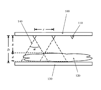
As can be appreciated by referring to Figure 1, the tissue thickness d, stand-
off
distance from the emitter panel to the tissue 6, and the separation between
the emitter
panel and the detector D are related by:
D = d + 6
The above relations can similarly be applied to maximal, actual and design
variables as well, as would be understood by thc skilled person. For instance,
in actual
use (during x-ray imaging), the variables may differ from the design
variables. Thus, the
method may further comprise a relation between the collimation angle, a, and
the other
variables in use satisfies the inequality:
rMactual
a > 2 tan-1 r
40 actual
in which:
is the actual stand-off distance of the emitter panel from the tissue
6 actual
placed between the emitter panel and the detector panel; and
M actual is a factor representative of a multiplicity of overlapping conelets
from adjacent x-ray emitters on a given part of the tissue.
M actual may be determined by solving the further equation:
A dactual
M actual = n
"actual
in which:
7
Date Recue/Date Received 2021-09-23
dactuat is the actual thickness of tissue placed between the emitter panel
and the detector panel; and
Dactuat is the actual emitter-detector panel separation, less than Dmax.
A lower limit for a may be given by 2 tan-1- -r6 (1 -
It will be appreciated that the above relations are not all independent.
Dmax may be determined based on an imaging modality. The method may further
comprise determining Dniax.
Dm ax may be determined by solving the further equation:
4dmax
Dmax = _________________________________________
A L4
in which:
dmax is a predetermined maximum thickness of tissue placed between the emitter
panel and the detector panel; and
Mmin is a predetermined minimum value of a factor representative of a
multiplicity of overlapping conelets from adjacent x-ray emitters on a given
part of the
tissue, wherein Mnan has a value between 1 and 4.
Dm ax may be between approximately 0.05m and 2m, in particular between
approximately 0.07m and lm, more particularly between approximately 0.08m and
0.5m,
for instance 0.1m, 0.2m, 0.4m, 0.48m and/or 0.5m. It may be between
approximately
0.2m and 0.4m.
dmax may be between approximately 0.01m and lm, in particular 0.05m and
0.4m, more particularly between approximately 0.1m and 0.3m, for instance
0.05m or
0.3m.
Mmin may be determined based on a consideration of the specific image
reconstruction approach used and the desired speed of imaging, where here the
speed
may include the complete process of image acquisition and processing. The
method may
further comprise determining Mmin.
Mini, may be determined based on a minimum value of Mactual -
In general, a larger Mmin corresponds to more information available for image
reconstruction and a longer period being required to obtain the image. Malin
may be
between approximately 1 and 3.9, in particular between approximately 1 and
3.7, more
particularly between approximately 1 and 3.6, for instance approximately 1.5,
2, 3 or 3.6.
8
Date Recue/Date Received 2021-09-23
BRIEF DESCRIPTION OF THE DRAWINGS
The above and other characteristics, features and advantages of the present
invention will become apparent from the following detailed description, taken
in
conjunction with the accompanying drawings, which illustrate, by way of
example, the
principles of the invention. This description is given for the sake of example
only, without
limiting the scope of the invention. The reference figures quoted below refer
to the
attached drawings.
Figure 1 is a schematic cross-sectional representation of an emitter array in
use.
Figure 2 is a schematic cross-sectional representation of an emitter array in
use.
Figure 3 is a schematic plan-view representation of an emitter array.
DETAILED DESCRIPTION
The present invention will be described with respect to certain drawings but
the
invention is not limited thereto but only by the claims. The drawings
described are only
schematic and are non-limiting. Each drawing may not include all of the
features of the
invention and therefore should not necessarily be considered to be an
embodiment of the
invention. In the drawings, the size of some of the elements may be
exaggerated and not
drawn to scale for illustrative purposes. The dimensions and the relative
dimensions do
not correspond to actual reductions to practice of the invention.
Furthermore, the terms first, second, third and the like in the description
and in
the claims, are used for distinguishing between similar elements and not
necessarily for
describing a sequence, either temporally, spatially, in ranking or in any
other manner. It
is to be understood that the terms so used are interchangeable under
appropriate
circumstances and that operation is capable in other sequences than described
or
illustrated herein.
Moreover, the terms top, bottom, over, under and the like in the description
and
the claims are used for descriptive purposes and not necessarily for
describing relative
positions. It is to be understood that the terms so used are interchangeable
under
appropriate circumstances and that operation is capable in other orientations
than
described or illustrated herein.
It is to be noticed that the term "comprising", used in the claims, should not
be
interpreted as being restricted to the means listed thereafter, it does not
exclude other
elements or steps. It is thus to be interpreted as specifying the presence of
the stated
features, integers, steps or components as referred to, but does not preclude
the presence
9
Date Regue/Date Received 2021-09-23
or addition of one or more other features, integers, steps or components, or
groups
thereof. Thus, the scope of the expression "a device comprising means A and B"
should
not be limited to devices consisting only of components A and B. It means that
with
respect to the present invention, the only relevant components of the device
are A and B.
Similarly, it is to be noticed that the term "connected", used in the
description,
should not be interpreted as being restricted to direct connections only.
Thus, the scope
of the expression "a device A connected to a device B" should not be limited
to devices
or systems wherein an output of device A is directly connected to an input of
device B.
It means that there exists a path between an output of A and an input of B
which may be
a path including other devices or means. "Connected" may mean that two or more
elements are either in direct physical or electrical contact, or that two or
more elements
are not in direct contact with each other but yet still co-operate or interact
with each other.
Reference throughout this specification to "an embodiment" or "an aspect"
means that a particular feature, structure or characteristic described in
connection with
the embodiment or aspect is included in at least one embodiment or aspect of
the present
invention. Thus, appearances of the phrases "in one embodiment", "in an
embodiment",
or "in an aspect" in various places throughout this specification are not
necessarily all
referring to the same embodiment or aspect, but may refer to different
embodiments or
aspects. Furthermore, the particular features, structures or characteristics
of any
embodiment or aspect of the invention may be combined in any suitable manner,
as
would be apparent to one of ordinary skill in the art from this disclosure, in
one or more
embodiments or aspects.
Similarly, it should be appreciated that in the description various features
of the
invention are sometimes grouped together in a single embodiment, figure, or
description
thereof for the purpose of streamlining the disclosure and aiding in the
understanding of
one or more of the various inventive aspects. This method of disclosure,
however, is not
to be interpreted as reflecting an intention that the claimed invention
requires more
features than are expressly recited in each claim. Moreover, the description
of any
individual drawing or aspect should not necessarily be considered to be an
embodiment
of the invention. Rather, as the following claims reflect, inventive aspects
lie in fewer
than all features of a single foregoing disclosed embodiment. Thus, the daims
following
the detailed description are hereby expressly incorporated into this detailed
description,
with each claim standing on its own as a separate embodiment of this
invention.
Date Recue/Date Received 2021-09-23
Furthermore, while some embodiments described herein include some features
included in other embodiments, combinations of features of different
embodiments are
meant to be within the scope of the invention, and form yet further
embodiments, as will
be understood by those skilled in the art. For example, in the following
claims, any of the
claimed embodiments can be used in any combination.
In the description provided herein, numerous specific details are set forth.
However, it is understood that embodiments of the invention may be practised
without
these specific details. In other instances, well-known methods, structures and
techniques
have not been shown in detail in order not to obscure an understanding of this
description.
In the discussion of the invention, unless stated to the contrary, the
disclosure of
alternative values for the upper or lower limit of the permitted range of a
parameter,
coupled with an indication that one of said values is more highly preferred
than the other,
is to be construed as an implied statement that each intermediate value of
said parameter,
lying between the more preferred and the less preferred of said alternatives,
is itself
preferred to said less preferred value and also to each value lying between
said less
preferred value and said intermediate value.
The use of the term "at least one" may mean only one in certain circumstances.
The principles of the invention will now be described by a detailed
description of
at least one drawing relating to exemplary features of the invention. It is
clear that other
arrangements can be configured according to the knowledge of persons skilled
in the art
without departing from the underlying concept or technical teaching of the
invention, the
invention being limited only by the terms of the appended claims.
Figure 1 shows an emitter array 100 including a plurality of emitter elements
110.
Each emitter element 110 is configured to emit x-rays 140 over a collimation
angle a.
The emitter array 100 is shown in use such that x-rays 140 from the emitter
elements 110
may pass through a body 120 having an approximate thickness d, spaced a
distance 8 from
the emitter array 100, to be detected by a detector panel 130 that is spaced a
distance D
from the emitter array 100.
Figure 2 shows an emitter array 200 including a first and second plurality of
emitter elements (not shown). X-rays 240 (shown in solid lines) from an
emitter element
in the first plurality of emitter elements are arranged such that they do not
overlap with
x-rays from adjacent emitter elements in the first plurality of emitter
elements before
11
Date Recue/Date Received 2021-09-23
arriving at a detector panel 230 (after passing through tissue to be examined
220). This
prevents multiple images being formed of a single feature in the tissue 220.
Similarly, x-
rays 250 (shown in dotted lines) from an emitter element in the second
plurality of emitter
elements are arranged such that they do not overlap with x-rays from adjacent
emitter
elements in the second plurality of emitter elements before arriving at a
detector panel
230 (after passing through tissue to be examined 220). By using each plurality
of emitter
elements separately (i.e. spaced in time, temporal separation), a greater
coverage of the
tissue 220 may be made. In the arrangement shown in figure 2, at least one
further
plurality of emitter elements may also be used to build complete coverage of
the tissue
220 in a similar way.
Figure 3 is a schematic plan-view representation of an emitter array 300. Each
emitter element 310 is arranged with its centre at node points of a grid of
equilateral
triangles. That is, the centres are located at points:
2r(k+lj, k,1 e z
where:
= (1
0)
(cos -1-71")
e2 =
sin ¨3
and Z denotes the set of integers such that the defined points fit on a given
panel.
This pattern is shifted such that the panel is covered homogenously by 48
exposures
enumerated by the formula
f + 4(g ¨ 1) + 16(h ¨ 1), (f = 1, ,4; g = 1, ,4; h = 1, ,3)
The centres of circles that are fired simultaneously in exposure (f, g, h) are
given
by:
¨1_ g-1 h ¨ 1
r( _______________________ 2f ei + e2 + 20_ + 2kTi. + 2/F2' )
where:
( cos -6-Th)
e3 = 71-
sin-6
The first 16 exposures (corresponding to h=1) are obtained by shifting the
parent
pattern to the nodes obtained by bisecting the grid of equilateral triangles
twice.
12
Date Recue/Date Received 2021-09-23
The second and third group of 16 exposures are centred where the first set of
exposures left holes (regions not covered by radiation). There are twice as
many holes as
disks in any given exposure, which leads to the three sets of 16.
Note that all emitters except those near the boundary of the panel are
equidistant
to their six nearest neighbours, the distance being (
:12).
We call this distance emitter pitch, while we refer to r as the emitter scale.
The
emitter scale also has the interpretation as radius of the non-overlapping
disks of radiation
that reach the detector panel simultaneously in any given exposure. r may be
chosen such
that these disks are just touching.
13
Date Recue/Date Received 2021-09-23