Note: Descriptions are shown in the official language in which they were submitted.
CA 02963290 2017-04-06
WO 2016/070992
PCT/EP2015/002212
=
Electrical interface
The present invention relates to an electrical interface, in particular an
interposer,
comprising a first connection plane with at least one first contact surface
pair,
each of which comprises a first and second contact surface, and a second
connection plane with at least one second contact surface pair, each of which
comprises a third and a fourth contact surface, wherein for each of a first
and
second contact surface pair, a first electric connection electrically connects
the
first contact surface of the first connection plane to the third contact
surface of
the second connection plane, and a second electric connection electrically
connects the second contact surface of the first connection plane to the
fourth
contact surface of the second connection plane, according to the preamble of
claim 1.
In large computer systems it is usual that several processor boards, each
forming a server, in the form of populated printed circuit boards, also known
as
"blades", are connected electrically and mechanically via plug-in slots with a
so-
called "backplane'', which is itself also a populated printed circuit board.
For this
purpose, angle connectors are provided which establish contact between plug
connectors or connection points on the blades on the one hand and plug
connectors or connection points on the backplane on the other hand in order to
establish corresponding data transmission channels between the respective
blade and the associated backplane.
CA 02963290 2017-04-06
WO 2016/070992
PCT/EP2015/002212
2
However, the electrical connection via the angle connector gives rise to
various
different problems which affect the high-frequency signal transmission
properties
of the electrical connections. For example, the conductors in the printed
circuit
board plug connectors should all have an identical impedance of 85 Ohm.
However, due the geometrical circumstances, not all conductors in an angle
plug
connector have an identical geometric length, if these are arranged directly
on
the shortest paths running from the first plane to the second. However, phase
differences in the transmission of high-frequency signals via the conductors
of
the angle connector need to be avoided, for which reason the conductors are
frequently laid in a wavelike manner within the angle connectors, so that all
conductors have an identical geometric length and thus also electric length.
However, this has the disadvantage that the desired characteristic impedance
of
85 Ohm is not present at each point between two adjacent conductors due to the
distance changing in a wavelike manner. Since the conductors within a printed
circuit board plug connector influence one another, for example during the
differential transmission of high-frequency signals, this changing
characteristic
impedance over the course of the conductors leads to significant limitations
in
terms of the maximum transmittable bandwidth and bit rate,
The invention is based on the problem of improving an electrical interface of
the
aforementioned type such that high bandwidths and bit rates are achieved
during
the transmission of high-frequency signals.
According to the invention, this problem is solved through an electrical
interface
of the aforementioned type with the characterising features of claim 1,
Advantageous embodiments of the invention are described in the further claims.
According to the invention, in an electrical interface of the aforementioned
type,
the first electrical connection between the first and third contact surface
has a
specified first geometric length and the second electrical connection between
the
second and fourth contact surface has a specified second geometric length, the
first and second geometric length being different.
CA 02963290 2017-04-06
WO 2016/070992
PCT/EP2015/002212
3
This has the advantage that, with the electrical interface, runtime or phase
differences, for example due to circuits adjacent the electrical interface,
between
a first electrical signal component which is transmitted via the first and
third
contact surface and a second electrical signal component which is transmitted
via the second and fourth contact surface are deliberately influenced and in
particular compensated to a difference of zero.
In order to compensate runtime or phase differences of signals which are
transmitted via an electrical angle connector, the electrical interface is
designed
to be interposed between a flat end surface of an electrical angle connector
which has at least one conductor pair for the differential transmission of
data
signals and a connection point with contact surfaces on a printed circuit
board.
An arrangement of the contact surfaces in the manner of a star quad cable, or
configured to make contact with end surfaces of a star quad cable, is achieved
in
that two first and second contact surface pairs are provided, wherein the
first and
second contact surfaces of the two first contact surface pairs on the first
connection plane are arranged at the corners of a square such that a first and
second contact surface of a first contact surface pair are in each case
arranged
diagonally opposite one another, wherein the third and fourth contact surfaces
of
the two second contact surface pairs on the second connection plane are
arranged at the Corners of a square such that a third and fourth contact
surface
of a second contact surface pair are in each case arranged diagonally opposite
one another.
An identical compensation of runtime or phase differences for all conductors
or
contact surface pairs is achieved in that all first electrical connections
have an
identical geometric length relative to one another and that all second
electrical
connections have an identical geometric length relative to one another.
An electrical interface requiring little construction space is achieved in
that the
first and second connection plane are arranged parallel to one another.
CA 02963290 2017-04-06
WO 2016/070992
PCT/EP2015/002212
4
A geometric length for the second electrical connection with a value of
substantially zero is achieved in that the second electrical connection is a
through-connection running from the first to the second connection plane in a
direction perpendicular to the connection planes.
A particularly good impedance-controlled electrical interface is achieved in
that
the second and fourth contact surface of a first and second contact surface
pair
are arranged so as to align with one another in a direction perpendicular to
the
connection planes, wherein the first and third contact surface of a first and
second contact surface pair are spaced apart from one another in a direction
perpendicular to the connection planes.
A particularly electrically and mechanically simple and functionally reliable
structure is achieved in that a third plane is formed which is arranged
between
the first and second connection plane, wherein the first electrical connection
and
the second electrical connection are formed in the third plane.
A compact structure which can be controlled well electrically, particularly in
terms
of impedance, is achieved in that the third plane is formed parallel to the
first
and/or second connection plane.
A particularly simple and electrically functionally reliable runtime or phase
difference compensation is achieved in that the first electrical connection is
designed as a flat conductor track which runs parallel to the first and/or
second
connection plane.
The invention is explained in the following with reference to the drawing, in
which:
Fig. 1 shows an exemplary embodiment of an electrical interface according to
the invention in a view from above,
CA 02963290 2017-04-06
WO 2016/070992
PCT/EP2015/002212
Fig. 2 shows the electrical interface according to Fig. 1 in a side view,
Fig. 3 shows the electrical interface according to Fig. 1 in an isometric
view,
5 Fig. 4 shows the electrical interface according to Fig. 1 in a view from
above,
with the underside omitted,
Fig. 5 shows the electrical interface according to Fig. 1 in a view from
above,
with the upper side omitted, so that only the underside is illustrated from
above,
Fig. 6 shows the electrical interface according to Fig. 1 used with an angle
connector and
Fig. 7 shows a detail view of the angle connector according to Fig. 6.
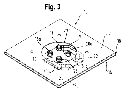
The preferred embodiment of an electrical interface 10 illustrated in Figs. 1
to 5
has a first connection plane 12, a second connection plane 14 and a third
plane
16 which are all oriented parallel to one another, wherein the third plane 16
is
arranged between the first and second connection plane 12, 14. Two first
contact
surface pairs 19, 19a, each with a first contact surface 18, 18a and a second
contact surface 20, 20a, are arranged in the first connection plane 12. Two
second contact surface pairs 23, 23a, each with a third contact surface 22,
22a
and a fourth contact surface 24, 24a, are arranged in the second connection
plane 14. In this context the term "plane" means a delimited level or flat
surface
considered as a two-dimensional object in three-dimensional space. In the
exemplary embodiment described in the following, the "planes" 12, 14, 16 are
flat
(i.e. without curvature), square surfaces.
The first contact surface 18 of one first contact surface pair 19 in the first
connection plane 12 is connected electrically with the third contact surface
22 of
a second contact surface pair 23 in the second connection plane 14 via a first
electrical connection 26. The second contact surface 20 of the first contact
CA 02963290 2017-04-06
WO 2016/070992
PCT/EP2015/002212
6
surface pair 19 in the first connection plane 12 is connected electrically
with the
fourth contact surface 24 of a second contact surface pair 23 in the second
connection plane 14 via a second electrical connection 28.
The first contact surface 18a of the other first contact surface pair 19a in
the first
connection plane 12 is connected electrically with the third contact surface
22a of
the other second. contact surface pair 23a in the second connection plane 14
via
a further first electrical connection 26a. The second contact surface 20a of
the
other first contact surface pair 19a in the first connection plane 12 is
connected
electrically with the fourth contact surface 24a of the other second contact
surface pair 23a in the second connection plane 14 via a further second
electrical connection 28a.
In other words, in the interface 10, one first contact surface pair 19 in the
first
connection plane 12 is transposed to one second contact surface pair 23 in the
second connection plane 14 and the other first contact surface pair 19a in the
first connection plane 12 is transposed to the other second contact surface
pair
23a in the second connection plane 14.
The two first electrical connections 26, 26a are flat conductors which are
arranged in the .third plane 16 and run substantially parallel to the first
and
second connection plane 12, 14. The two second electrical connections 28, 28a
are through-connections running from the first connection plane 12, through
the
third plane 16, to the second connection plane 14 and run substantially
perpendicular to the three planes 12, 14, 16. The geometric lengths of the
first
electrical connections 26, 26a are identical and at the same time longer than
the
geometric lengths of the respective second electrical connections 28, 28a, The
geometric lengths of the second electrical connections 28, 28a are also
identical
to one another.
The first and second contact surfaces 18, 18a, 20, 20a in the first connection
plane 12 are arranged at the corners of an imaginary square 40 (Fig. 4) in the
first connection plane 12 such that the contact surfaces 18, 20 or 18a, 20a of
a
CA 02963290 2017-04-06
WO 2016/070992
PCT/EP2015/002212
7
contact surface pair 19 or 19a are arranged diagonally opposite one another.
Thus, in the illustrated embodiment, the first and second contact surface 18,
20
of one first contact surface pair 19 are arranged diagonally opposite one
another
in relation to the imaginary square 40 (Fig. 4) and the first and second
contact
surface 18a, 20a of the other first contact surface pair 19a are arranged
diagonally opposite one another in relation to the imaginary square 40 (Fig.
4).
Analogously, in the second connection plane 14 the third and fourth contact
surfaces 22, 24 or 22a, 24a of the second contact surface pairs 23 or 23 are
arranged diagonally opposite one another at the corners of an imaginary square
50 (Fig. 5) in the second connection plane 14. Thus, in the illustrated
embodiment the third and fourth contact surface 22, 24 of a second contact
surface pair 23 are arranged diagonally opposite one another in relation to
the
imaginary square 50 (Fig. 5) and the third and fourth contact surface 22a, 24a
of
the other second contact surface pair 23a are arranged diagonally opposite one
another in relation to the imaginary square 50 (Fig. 5),
The arrangement or the so-called "footprint" of the first and second contact
surfaces 18, 20 and 18a, 20a in the first connection plane 12 described above
is
transposed via the invented interface 10 to the arrangement or "footprint" of
the
third and fourth contact surfaces 22, 24 or 22a, 24a in the second connection
plane 14 described above with identical dimensions and arrangement, but
displaced in a direction perpendicular to the planes 12, 14, 16. At the same
time,
by means of the first electrical connection 26, 26a providing an electrical
connection between a first contact surface 18 and 18a and a third contact
surface 22, 22a, the geometric paths and thus the electrical paths for a
transmitted high-frequency signal are lengthened in comparison with the second
electrical connections 28, 28a between a second contact surface 20, 20a and a
fourth contact surface 24, 24a.
The arrangement of the contact surfaces 18/20, 18a/20a, 22/24, 22a/24a of the
contact surface pairs 19, 19a, 23, 23a corresponds to the arrangement of
conductors in a so-called star quad transmission cable, which is in particular
CA 02963290 2017-04-06
WO 2016/070992
PCT/EP2015/002212
8
suitable for the differential transmission of high-frequency signals. The
interface
according to the invention hereby serves as an interposer between an angle
connector 30, as illustrated in Fig. 6, and a printed circuit board (not
illustrated).
As can be seen from Fig. 7, the angle connector illustrated in Fig. 6 contains
two
pairs of conductors 32, 34 and 32a, 34a, which are arranged in the manner of a
star quad cable, wherein in each cross section of the angle connector 30 the
conductors are arranged at the corners of a imaginary square 36, wherein two
conductors 32, 34 or 32a, 34a of a conductor pair are always arranged
diagonally opposite one another in relation to the imaginary square 36. In
other
words, on the one hand the conductors 32, 34 are arranged diagonally opposite
one another in relation to the imaginary square 36 and on the other hand the
conductors 32a, 34a are arranged diagonally opposite one another in relation
to
the imaginary square 36.
The angle connector 30 shown in Fig. 6 has a angle of 90 , so that the
conductors 34, 34a have a shorter geometric length, from one end to the other
end of the angle connector 30, than the conductors 32, 32a, since the
conductors 34, 34a run along an inside track and the conductors 32, 32a run
along an outside track around the 90 angle of the angle connector 30. The
interface 10 is arranged, as a so-called interposer, between the angle
connector
and the (not illustrated) printed circuit board such that the conductors 34,
34a
with the shorter geometrical paths in the angle connector 30 each meet on the
two first contact surfaces 18 and 18a in the first connection plane 12, so
that one
first contact surface 18 makes electrical contact with the conductor 34 and
the
25 other first contact surface 18a makes electrical contact with the
conductor 34a.
At the same time, the conductor 32 makes electrical contact with one second
contact surface 20 and the conductor 32a makes electrical contact with the
other
second contact surface 20a in the first connection plane 12. While the
electrical
signals transmitted via the conductors 32 and 32a are transmitted directly
from
30 the second contact surfaces 20, 20a by means of the through-connections
28,
28a, by the shortest path through the interface 10, to the fourth contact
surfaces
24, 24a in the second connection plane 14, the signals transmitted from the
conductors 34, 34a are transmitted via the Jong first electrical connections
26,
CA 02963290 2017-04-06
W02016/070992
PCT/EP2015/002212
9
26a to the third contact surfaces 22, 22a. The first electrical conductors 26,
26a
are thereby so designed in terms of their geometric length that a phase or
runtime shift relative to the signals transmitted on the other conductors 32,
32a is
compensated. In other words, a phase or runtime shift between the
geometrically
shorter conductors 34, 34a in the angle connector 30 relative to the
geometrically
longer conductors 32, 32a in the angle connector 30 is compensated by means
of the first electrical connection 26, 26a. The compensation in each case
takes
place for a conductor pair 32, 34 or 32a, 34a arranged diagonally opposite one
another in the angle connector 30, so that the phase or runtime shift of a
signal
in the conductor 34 relative to the conductor 32 is compensated through one
first
electrical connection 26 and the phase or runtime shift of a signal in the
conductor 34a relative to the conductor 32a is compensated through the other
first electrical connection 26a.
Each conductor 32, 34, 32a and 34a has a copper wire 42 with a diameter of for
example 0.3 mm as well as a coating 44, for example made of Teflon. The four
conductors 32, 34, 32a and 34a are embedded in a dielectric 46, which for
example has a diameter of 1.7mm. The dielectric is for example manufactured
from the material polyoxymethylene (abbreviation: POM).
The connection planes 12, 14 are for example manufactured from an epoxy resin
laminate with the designation NELCOE) N4000-13 and have a thickness of for
example 4 mm.