Note: Descriptions are shown in the official language in which they were submitted.
CA 02964326 2017-04-10
WO 2016/064725 PCT/US2015/056204
METHOD AND APPARATUS FOR INTRINSIC POWER FACTOR CORRECTION
CROSS-REFERENCE TO RELATED APPLICATIONS
[0001] The present application claims priority to U.S. Provisional
Patent Application
No. 62/065,889, filed October 20, 2014. The contents of that application are
hereby incorporated
by reference.
TECHNICAL FIELD
[0002] The invention relates to the transmission of electrical energy
by means of
resonant induction. More specifically, the invention relates to a method of
wireless transmission
that provides a near unity power factor, low harmonic distortion load at the
line connection point
without employing specific power factor correction circuitry. Instead, the
apparatus described
herein provides a low harmonic distortion, near unity power factor without the
need for a specific
power factor correction stage thereby reducing component cost, apparatus size,
and power
conversion losses.
BACKGROUND
[0003] Inductive power transmission has many important applications spanning
many
industries and markets. Although the disclosure contained here contemplates
the use of this
invention to applications requiring relatively high power (in excess of 100
watts), the potential
list of power applications is not limited and this invention can be applied to
a wide range of
power requirements.
[0004] Figure 1 shows a conceptual representation of a prior art
resonant inductive
power transmission system 10. As illustrated, a source of alternating, line
frequency electrical
energy is provided on AC line 12 and converted into direct current with a line
frequency rectifier
14 and shunt capacitor ripple filter 16. A DC-AC inverter 18 converts the
direct current energy
into high frequency alternating current which is applied by means of a
resonating network 20 to
the primary side induction coil 22. Typical operating frequencies are in the
range of 15-50 kHz.
[0005] Magnetic coupling between the primary side induction coil 22
and the
secondary side induction coil 24 transfers primary side energy to the
secondary side where it is
rectified by high frequency rectifier 26, ripple filtered by ripple filter 28
and used to charge a
1
CA 02964326 2017-04-10
WO 2016/064725 PCT/US2015/056204
remotely located battery 30. A resonating network 32 resonates the secondary
side induction coil
24 thereby enabling maximum current flow and maximum energy transfer.
[0006] The nature of the load presented to the AC line connection in
the circuit of
Figure 1 is determined by the line rectifier - shunt ripple filter capacitor
combination. In
operation, the line rectifier current is zero unless the instantaneous
rectified line voltage exceeds
the shunt capacitor voltage. This means that the rectifier current is not
sinusoidal but is instead a
narrow pulse that occurs just before the line voltage sinusoid reaches its
maximum value.
Because the rectifier current is a narrow pulse instead of a sinusoid, it
contains considerable
harmonic content. The associated line frequency harmonic currents are harmful
to electric power
distribution components and also to other loads connected to the distribution
system and are for
that reason restricted to low amplitude by utility or government regulation.
[0007] Another difficulty is the fact that the line frequency rectifier
current peak occurs
before the line frequency voltage maximum. This means that the fundamental
harmonic
component of the line frequency rectifier current pulse leads the line
frequency voltage sinusoid
creating an undesirable leading current factor which is also subject to
regulatory restrictions.
Increasing the capacitance of the shunt line frequency ripple filter capacitor
16 reduces the
magnitude of the direct current line frequency ripple but also undesirably
increases the
magnitude and decreases the width of the rectifier current pulse, thereby
increasing undesirable
line frequency harmonic distortion and unacceptable line power factor.
[0008] The problem then is how to convert line frequency alternating current
into direct
current while drawing an in-phase, sinusoidal current from the line voltage
source. Figure 2
shows the conventional solution to this problem, namely, the addition of a
power factor
correction stage 34. Note that power factor correction in this usage implies
both the elimination
of rectifier created line frequency harmonic distortion as well as alignment
of line frequency
voltage and current sinusoids.
[0009] The power factor correction stage 34 shown in Figure 2 consists of a DC-
to-DC
boost converter although buck and boost-buck converters topologies can be
employed as well. A
shunt switching device depicted in Figure 2 as a shunt field effect transistor
36 controls inductor
current and therefore AC line current by means of pulse duration. When the
shunt transistor 36
is on, inductor current ramps up at a rate proportional to the instantaneous
rectified line voltage.
Energy stored in the inductor 38 is dumped into the shunt filter capacitor 16
through the series
2
CA 02964326 2017-04-10
WO 2016/064725 PCT/US2015/056204
diode 40 when the shunt transistor 36 turns off. A control circuit 42 monitors
the rectified line
current and continuously adjusts the transistor conduction intervals such that
the rectified line
current remains proportional to the line voltage. In this way, the line
frequency rectifier current is
made to be half-cycle sinusoidal and proportional to the line voltage
amplitude, harmonic
distortion is forced to zero, the power factor is forced to unity, and the DC-
AC inverter supply
voltage is held essentially constant.
[0010] However, there are at least two distinct disadvantages to the
conventional
method of power factor correction depicted in Figure 2. Namely, the added
power conversion
stage increases the cost and the volume of the apparatus and also introduces
unwanted energy
conversion losses. It is desired to provide a near unity power factor, low
harmonic distortion
load at the line connection point in a resonant inductive power transmission
system without
employing such specific power factor correction circuitry. The invention
addresses this need in
the art.
SUMMARY
[0011] The invention addresses the above mentioned limitations of the
prior art by
changing the operating parameters of the resonant induction wireless power
apparatus so that it
intrinsically provides a low harmonic distortion, near unity power factor line
load without the
need of an additional energy conversion power factor correction. The post-
rectifier, line
frequency ripple filter, and shunt capacitor of conventional circuits are
eliminated and the DC-to-
AC inverter is powered not by smoothed, constant value DC voltage but by a
half-sinusoidal
voltage derived from the full wave rectification of the line sinusoid.
[0012] In an exemplary embodiment, the envelope of the high frequency
rectangle
wave developed by the DC-AC inverter is no longer constant but varies
continuously in a half-
sinusoidal fashion. The conventional transmission coil pair is combined with
resonating
capacitors with values specifically selected such that the resonant
transmission coil pair becomes
a resonant impedance inverter having 90 degrees of transmission phase shift
that forces the
system load current magnitude, and therefore the AC line current, to be
proportional and in phase
with the AC line voltage, thus ensuring near unity AC load power factor and
low AC line
harmonic current content.
3
CA 02964326 2017-04-10
WO 2016/064725 PCT/US2015/056204
[0013] On the secondary side of the wireless power transmission coil
pair, a rectifier
rectifies the transmission frequency sinusoid. A post-rectifier filter removes
the inverter
frequency ripple and delivers line frequency, half-sinusoid current to the
constant DC voltage
load. In a three phase AC line source embodiment, the current delivered to the
load is the sum of
three rectified sinusoids offset from each other by 120 degrees and therefore
has reduced line
frequency ripple.
[0014] In the exemplary embodiment, the invention provides an apparatus that
maintains
near unity AC line power factor and low AC line harmonic current content. The
system
includes, on the transmission side, a line frequency rectifier not followed by
a line frequency
ripple filter, a DC-to-AC inverter that inverts the rectified AC line
frequency to an envelope
modulated high frequency rectangular waveform with an amplitude that varies
continuously in a
half-sinusoidal fashion, a transmission coil pair that is combined with
resonating capacitors with
values specifically selected such that the resonant transmission coil pair
becomes a resonant
impedance inverter having 90 degrees of transmission phase shift, and a
primary side induction
coil. On the receiving side, the system includes a transmission frequency
rectifier and associated
transmission frequency ripple filter that provides half-sinusoidal, non-
alternating DC current to
the receiving side load.
[0015] In another exemplary embodiment, the invention is used in applications
where the
power flows from a DC power source to an AC load. In such an embodiment, the
intrinsic
power factor correction apparatus includes a DC power source, a shunt ripple
filter capacitor that
provides line frequency ripple filtering of an output of the DC power source,
a DC-to-AC
inverter that converts a line frequency ripple filtered DC voltage from an
output of the shunt
ripple filter capacitor to an output square wave voltage, an impedance
inverter that converts the
output square wave voltage to a sinusoidal wave at a frequency of the DC-to-AC
inverter that is
envelope modulated by a line frequency sinusoid to form a bipolar sinusoidal
envelope, a
secondary side rectifier that converts the bipolar sinusoidal envelope into a
unipolar half-
sinusoidal envelope, a de-rectification network that inverts a polarity of
every other cycle of the
unipolar half-sinusoidal envelope to generate a sinusoidal waveform, and an AC
load that
receives the sinusoidal waveform. As in the case of the AC source and DC load,
the impedance
inverter raises a secondary side voltage under conditions of light loading so
as to force line
frequency source current from the DC power source and a current at the AC load
to be
4
CA 02964326 2017-04-10
WO 2016/064725 PCT/US2015/056204
proportional so as to maintain near unity line load power factor and low
harmonic current
distortion. In an exemplary embodiment, this is accomplished by using a Terman
impedance
inverting network as the impedance network so as to provide a voltage
transformation that varies
with an instantaneous load voltage at the secondary side of the Terman
impedance inverting
network. A ripple filter network also may be provided to remove high frequency
ripple from the
unipolar half-sinusoidal envelope before it is applied to the de-rectification
network. The de-
rectification network itself may include power semiconductor switches in a
half wave or full
wave bridge configuration.
[0016] In yet another embodiment, a three phase AC grid load is accommodated
using
three independent DC-to-AC inverter strings where each string drives one of
the three AC
constant voltage loads that together constitute an AC three phase constant
voltage load. An
isolation transformer may be used in each string to provide galvanic isolation
between the DC
power source and the AC load. Also, the DC power source may include three
equal voltage
independent DC power sources or three DC source nodes may be tied together and
fed by a
single DC power source.
DETAILED DESCRIPTION OF DRAWINGS
[0015] The foregoing and other beneficial features and advantages of
the invention
will become apparent from the following detailed description in connection
with the attached
figures, of which:
[0016] Figure 1 is a conceptual representation of a prior art resonant
induction
wireless power transfer system without power factor correction.
[0017] Figure 2 is a conceptual representation of a prior art resonant
induction
wireless power transfer system with added power factor correction circuitry.
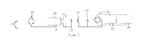
[0018] Figure 3 is a conceptual representation of an embodiment of the
invention.
[0019] Figure 4 is a representation of a Terman Tee configuration
impedance
matching network.
[0020] Figure 5 shows the conversion of a coupled inductor Tee wireless
power coil
pair equivalent circuit into a resonant impedance inverter.
[0021] Figure 6 is schematic diagram of a circuit used for computer
circuit analysis of
the embodiment of Figure 3.
CA 02964326 2017-04-10
WO 2016/064725 PCT/US2015/056204
[0022] Figure 7 is a graph showing linear results of spice stimulation
generated by
computer modeling of the load current versus inverter source voltage, at
resonance and off
resonance.
[0023] Figure 8 is a conceptual representation of the application of
the invention to
three phase line frequency sources using three isolated inverters and inverter
output voltage
summation.
[0024] Figure 9 illustrates an alternative embodiment with the
summation transformer
of Figure 8 replaced by a primary side induction coil implemented as three
independent, co-
located, induction coils sharing a common magnetic core.
[0025] Figure 10 illustrates a conceptual block diagram and associated
voltage
waveforms for a DC-to-AC inverter based useful for applications in which power
flows instead
in the opposite direction from DC-source to ac-load with the apparatus
providing a near unity
power factor AC source.
[0026] Figure 11 illustrates an embodiment for accommodating a three
phase AC grid
load using three independent DC-to-AC inverter strings as in Figure 9, where
each string drives
one of the three AC constant voltage loads that together constitute an AC
three phase constant
voltage load.
DETAILED DESCRIPTION OF ILLUSTRATIVE EMBODIMENTS
[0027] The present invention may be understood more readily by
reference to the
following detailed description taken in connection with the accompanying
figures and examples,
which form a part of this disclosure. It is to be understood that this
invention is not limited to the
specific products, methods, conditions or parameters described and/or shown
herein, and that the
terminology used herein is for the purpose of describing particular
embodiments by way of
example only and is not intended to be limiting of any claimed invention.
Similarly, any
description as to a possible mechanism or mode of action or reason for
improvement is meant to
be illustrative only, and the invention herein is not to be constrained by the
correctness or
incorrectness of any such suggested mechanism or mode of action or reason for
improvement.
[0028] A detailed description of illustrative embodiments of the
present invention will
now be described with reference to Figures 3-11. Although this description
provides a detailed
6
CA 02964326 2017-04-10
WO 2016/064725 PCT/US2015/056204
example of possible implementations of the present invention, it should be
noted that these
details are intended to be exemplary and in no way delimit the scope of the
invention.
[0029] As will now be explained, the system described herein and shown
in Figure 3
is explained in the context of a resonant induction wireless battery charging
apparatus, although
it will become apparent to those skilled in the art that the invention has
numerous other
applications. It will be appreciated by those skilled in the art that the
embodiment of Figure 3
departs from conventional resonant induction wireless battery charging
practice in a number of
ways. For example, battery charging current is not constant; it varies in a
half-sinusoidal or
rectified sinusoidal fashion. In this way, battery charging current is
proportional to and in phase
with a single phase AC line voltage sinusoid source. The secondary side
rectifier load
impedance is understood to be non-linear, behaving as a constant voltage load
with a small
Thevenin resistance. No current flows through the secondary side rectifier
unless the applied
alternating voltage exceeds the battery terminal voltage. The primary side,
secondary side
induction coil pair 22, 24 and associated resonating capacitors 20, 44 can be
configured to
function as a voltage step up network under conditions of light loading. Such
resonant LC
networks are intrinsically high Q under light load conditions and large
voltage step up ratios are
possible at the resonant frequency.
[0030] During the period of no rectifier current flow, the resistive losses in
the secondary
side resonant circuit are zero, the instantaneous loaded Q is very high, and
significant voltage
transformation occurs. Under such instantaneous no-load conditions, the
resonant circuit output
voltage applied to the secondary side rectifier 26 increases until it exceeds
the battery terminal
voltage and battery current begins to flow. With proper design, the secondary
side battery
charging current can be made to flow throughout the duration of the line
frequency half-cycle
and be proportional to the absolute value of the AC line voltage, thereby
presenting a low
distortion, unity power factor load to the AC line frequency source without
using a specific
power factor correction stage.
[0031] The invention described herein makes use of an impedance inverter that
provides
a voltage transformation that varies continuously as a function of the
instantaneous battery
terminal impedance as required to maintain proportionality between the line
current and the line
voltage over each line half-cycle. As known to those skilled in the art, an
impedance inverter is a
7
CA 02964326 2017-04-10
WO 2016/064725 PCT/US2015/056204
bi-directional two-port network in which a low impedance applied to one port
creates a high
impedance at the other port.
[0032] A k/4 transmission line transformer is an example of an impedance
inverter
implementation. Impedance inverter realizations are not limited to
transmission line
implementations. For example, there are multiple, lumped circuit
configurations including
ladder circuit networks. The invention makes use of a three element Tee
impedance matching
network as described by Terman (Radio Engineers handbook, First Edition,
McGraw Hill, 1943)
and shown in Figure 4. Terman impedance matching network reactances are found
as follows:
. R1 Cos fl ¨ IR1 R2 . R2 COS fl ¨ IR1 R2 VR1 R2
Z1 = ¨J _____________________ Z2 = j __________________ Z3 = j ____
Sin fl Sin fl Sin fl
where R1 is the two port source impedance, R2 is the two port load impedance,
and 0 is the phase
shift through the network in radians. The Tee impedance matching network
functions as an
impedance inverting network when designed to have a 90 degree, 1131 = n/2
transmission phase
shift. For 1131 = n/2 the reactance design equations simplify to:
Zi = Z2 = ¨Z3 = ¨j \Mt R2
[0033] In an exemplary embodiment, the values of R1 and R2 are not
constant but vary
continuously during each rectified half-cycle. The geometric product VR1 R2 is
constant and the
three network reactances have equal magnitude. This observation is used in the
subsequent
design of the resonant induction coil matching networks.
[0034] Figure 5 shows how a resonant induction wireless power coil pair
can be
transformed into a resonant Terman impedance inverter. Figure 5A shows the
wireless power
coil pair equivalent circuit of a wireless power transmission coil pair having
a coupling
coefficient of .385 at 19 kHz. The primary and secondary side winding
inductances of 130 iLtH
and the mutual inductance of 50 iLtH have reactances of +j17.9 and +j5.97,
respectively, at 19
kHz.
[0035] In Figure 5B, resonating capacitors 46, 48 are added to the
network series arms
of the equivalent circuit of Figure 5A. The reactance is selected to
completely cancel the
reactance of the series inductors Z1, Z2 at 19 kHz and to add an additional
series capacitive
8
CA 02964326 2017-04-10
WO 2016/064725 PCT/US2015/056204
reactance with the same magnitude as the reactance of the shunt, mutual
inductance element Z3
also at 19 kHz. The resulting network in Figure 5C is an impedance inverting
two-port
equivalent circuit incorporating a wireless power transfer, coupled inductor
pair.
[0036] The impedance inverting network of Figure 5C reduces or
eliminates inductive
wireless power transfer line current harmonic distortion as follows. Just
after the line voltage
zero-crossing, the magnitude of the rectified line voltage and the magnitude
of the inverter
voltage output is small. Rectified current provided to the vehicle battery 30
is zero or very small.
The impedance on the secondary side of the Terman impedance inverter is very
high; therefore,
the impedance on the primary side of the impedance inverter is very low. The
impedance
inverter sees a low impedance load and supplies substantial primary side
current. The secondary
side voltage increases until it exceeds the battery voltage. Battery charge
current starts to flow,
the impedance seen by the inverter increases, and the system stabilizes with
moderate line
current, moderate inverter current, and moderate battery charging current.
[0037] Near the peak of the line voltage cycle, the magnitude of the
rectified line
voltage and the magnitude of the impedance inverter voltage output is large.
Rectified current
provided to the vehicle battery is large as well. The impedance on the
secondary side of the
Terman impedance inverter is low; therefore, the impedance on the primary side
of the
impedance inverter is relatively high. The compensational action of the
impedance inverter
makes the line current and the battery charging current proportional to the
magnitude of the line
voltage, exactly the condition required for unity power factor and zero
harmonic distortion. A
conventional line filter network may be used to suppress inverter switching
frequency transients.
[0038] Figure 6 shows a schematic of an electronic circuit representing
a resonant
induction wireless power apparatus of the type illustrated in Figure 3 for
which the transfer coil
pair 22, 24 has been converted into a resonant impedance inverter following
the method outlined
in Figure 5 that was subjected to time domain computer circuit analysis. The
mutually coupled,
wireless power induction coils, represented by their equivalent Tee circuit
having primary and
secondary side winding inductances of 130 iLtH and a mutual inductance of 50
01, is transformed
into a resonant impedance inverting network 50 following the method described
with respect to
Figure 5. The AC voltage source 52 represents the output voltage of the
primary side inverter
18. The secondary side high frequency rectifier 26 and associated high
frequency ripple current
filter 28 are shown. The secondary side battery charging load 30 is
represented by a direct
9
CA 02964326 2017-04-10
WO 2016/064725 PCT/US2015/056204
current voltage source having a small Thevenin resistance representing battery
internal
resistance.
[0039] The inverter output voltage amplitude varies in proportion to
the rectified, but
not filtered, line frequency voltage. In order to determine the load current
as a function of the
inverter voltage, a computer simulation was conducted. Time domain circuit
simulation was
conducted for multiple values of inverter output voltage ranging from zero
volts to the peak
value of the rectified line voltage. The corresponding load current is graphed
in Figure 7 as a
function of the inverter, rectified sine supply voltage.
[0040] As shown in Figure 7, with the AC voltage source frequency set
to 19 kHz, the
network resonant frequency, battery charging current is linear and
proportional to the inverter
source voltage. It is important to note battery charging current linearity is
maintained even for
line source voltages much less than the battery open circuit terminal voltage,
a consequence of
the voltage transformation properties of a resonant circuit when lightly
loaded. The linear curve
of Figure 7 shows the desirable condition of secondary side load current, and
therefore inverter
supply current and line current being proportional to line voltage, a
condition that insures low
levels of line frequency harmonic distortion and unity line frequency power
factor. When
operated above and below the impedance inverter resonant frequency, at 17, 18
and 20 kHz as
indicated on Figure 7, the line voltage/line current relationship is no longer
proportional at low
line voltages resulting in line current harmonic distortion and degraded line
power factor. When
operated at the impedance inverter resonant frequency, current varies in a
half-sinusoidal or
rectified sinusoidal fashion.
[0041] Conventionally, battery charging is mediated by a battery
management system
that monitors and controls battery charging current and maximum battery
voltage as well as other
relevant parameters such as temperature, sometimes for the battery as a whole
but also for
individual cells. In current practice, battery/cell management systems require
the use of DC
charging current and will likely malfunction in the presence of half-
sinusoidal charging current.
This difficulty is eliminated by modifying the battery management system to
respond to the RMS
charging current instead of the average or peak measurement methodology
employed
conventionally.
[0042] Effective battery charging requires charging current magnitude
be altered
according to the battery state of charge as controlled by the battery charging
algorithm. In an
CA 02964326 2017-04-10
WO 2016/064725 PCT/US2015/056204
exemplary embodiment of the invention, maximum battery charging current
magnitude is set by
the design of the impedance inversion network and by the magnitude of the
rectified, half-
sinusoidal line voltage that supplies the inverter 18. Further control
(reduction) of battery
charging current is obtained by pulse width modulation of the inverter 18, by
inverter pulse
phasing, by inverter pulse dropping and by active control of the secondary
side rectifier 26.
These control methods employed individually or in combination enable effective
control of
charging current magnitude while maintaining low harmonic distortion, near
unity power factor.
[0043] While low to medium power wireless power systems operate from single
phase
power connections, high power systems generally require a three phase
connection. Even though
a rectified single phase sinusoid source has a large ripple component, the sum
of three rectified
sinusoidal sources, with each sinusoid displaced by 120 degrees, is much
smaller. Reduced
charging ripple current is sometimes desirable for compatibility with battery
management system
circuitry and for reduction of the peak to average charging current ratio in
order to limit battery
resistive losses during fast charging.
[0044]
Figure 8 shows an embodiment of the invention implemented with a three
phase line voltage source 54. Each phase has a separate rectifier 14 and
inverter 18. The three
inverters switch synchronously and the inverter outputs are combined by a
summing transformer
56 that can be three physically independent transformers or a single
transformer with six
windings on a common core with three phase partial flux cancellation allowing
more efficient
use of the core material. The summation transformer 56 also provides galvanic
isolation from
the AC line. Filters on the three phase lines (not shown in Figure 8) reject
inverter switching
frequency components resulting in a new unity, low harmonic distortion three
phase load. As in
prior art Figure 1, resonating network 20 connects the inverters 18 to the
primary side induction
coil 22. Magnetic coupling between the primary side induction coil 22 and the
secondary side
induction coil 24 transfers primary side energy to the secondary side where it
is rectified by high
frequency rectifier 26, ripple filtered by ripple filter 28 and used to charge
a remotely located
battery 30. A resonating network 44 resonates the secondary side induction
coil 24 thereby
enabling maximum current flow and maximum energy transfer.
[0045]
Figure 9 shows an alternative embodiment of Figure 8 where the summation
transformer 56 is replaced with the primary side induction coil 22 implemented
as three
independent, co-located, induction coils 23, sharing a common magnetic core
with a secondary
11
CA 02964326 2017-04-10
WO 2016/064725 PCT/US2015/056204
side induction coil that is connected to the secondary side rectifier. A
separate DC-AC inverter
18 and associated line frequency rectifier 14 drives each of the three primary
coils through
resonating networks 20. Power summation then occurs as the summation of
primary coil flux
fields such that dedicated combining transformers 56 are not required. Those
skilled in the art
will appreciate that the embodiment of Figure 9 eliminates the size, weight
and cost of the
combining transformers at the cost of adding two primary coils and two sets of
resonating
capacitors.
[0046] The power factor correction action of a Terman impedance inverter
network as
described herein can be advantageously employed in apparatus other than
resonant induction
wireless power transfer systems. Such applications include:
Wired ¨as opposed to wireless- battery charging;
Metal plating;
Electro-chemical processing such as electrolysis;
Induction heating;
Alternating current welding;
Gaseous discharge processes including fluorescent and arc lighting; and
Any other application providing direct current derived from an alternating
current source
to loads that can tolerate full wave rectified sinusoidal direct current.
[0047] In power factor control of wireless induction power transfer, the
Terman
impedance inversion network is absorbed into the Tee equivalent circuit of the
wireless transfer,
mutually coupled, air core coil pair, where one element of the Tee equivalent
circuit is the
mutual inductance. Those skilled in the art will appreciate that in non-
wireless power transfer
applications, the impedance inversion network can implemented at three
discrete, non-mutually
coupled components giving a significant increase in design flexibility.
[0048] In the applications discussed above, power flows from AC-source to DC-
load
with the apparatus providing a near unity power factor load to the AC source.
The teachings of
the invention apply equally to applications in which power flows instead in
the opposite direction
from DC-source to AC-load with the apparatus providing a near unity power
factor AC source.
A reversed power flow apparatus finds application as inverters feeding DC
power from
alternative energy sources such as photovoltaic panels and wind generators
into the 50 or 60 Hz
utility grid.
12
CA 02964326 2017-04-10
WO 2016/064725 PCT/US2015/056204
[0049] Figure 10 illustrates a conceptual block diagram and associated voltage
waveforms for a DC-to-AC inverter system useful for applications in which
power flows instead
in the opposite direction from DC-source to AC-load with the apparatus
providing a near unity
power factor AC source. As illustrated, the circuit of Figure 10 includes DC
power source 60
followed by a shunt ripple filter capacitor 62 that provides line frequency
ripple filtering. The
line frequency ripple filtered DC voltage is applied to a high frequency DC-to-
AC inverter 64.
High frequency in this context means high with respect to the line frequency.
The output square
wave voltage, 66, is applied to the input of a Terman impedance inverting
network 68 that
provides a voltage transformation that varies with the instantaneous load
voltage at the far side of
the impedance inversion network.
[0050] The waveform 70 at the output of the impedance inversion network 68 is
a
sinusoidal wave at the DC-to-AC inverter frequency, envelope modulated by a
line frequency
sinusoid. A high frequency rectifier 72 converts the bipolar sinusoidal
envelope into a unipolar,
half-sinusoidal envelope 74. A high frequency ripple filter network 76 removes
the high
frequency ripple giving a ripple free, line frequency half-sinusoidal waveform
78. A
derectification network 80 including power semiconductor switches in a half
wave or full wave
bridge configuration inverts the polarity of every other cycle of waveform 78
to generate
waveform 82, thereby allowing power flow into the constant AC voltage load 84,
which
represents an infinite grid.
[0051] A three phase AC grid load is accommodated as shown in Figure 11 with
three
independent DC-to-AC inverter strings, each string being the same as a single
phase inverter
string with isolation transformers 90 added. Each string drives one of the
three AC constant
voltage loads that together constitute an AC three phase constant voltage load
92. Isolation
transformers 90 provide galvanic isolation from the AC load 92. The DC source
94 can be three
equal voltage independent DC sources as shown in Figure 10 or the three DC
source nodes can
be tied together and fed by a single DC source. The filter capacitor 96
filters the 120 Hz half-
sinusoidal current variation that would otherwise be present at the DC source
node. The
elements and operation are otherwise the same as in the circuit configuration
of Figure 10.
[0052] Those skilled in the art will appreciate that the invention is
not limited to
wireless power device applications. In addition to wireless inductive charging
applications, the
invention may also be applied to uses outside of the transportation industry
such as AC induction
13
CA 02964326 2017-04-10
WO 2016/064725 PCT/US2015/056204
motors, motor controllers, resonant power supplies, industrial inductive
heating, melting,
soldering, and case hardening equipment, welding equipment, power
transformers, electronic
article surveillance equipment, induction cooking appliances and stoves, other
industrial
equipment, and other applications incorporating plug-in charging by a plug-in
charger, as well as
to other non-battery charging applications such as electrochemistry,
electroplating and all other
loads that can be operated with a half-sinusoidal current waveform from a
single phase line
source, or reduced ripple waveform that results from the summation of a
multiphase line source.
These and other such embodiments are considered to be included within the
scope of the
invention as defined by the following claims.
14