Note: Descriptions are shown in the official language in which they were submitted.
CA 02964421 2017-04-12
SUBSTRATE USED FOR LED ENCAPSULATION, THREE-DIMENSIONAL LED
ENCAPSULATION, BULB COMPRISING THREE-DIMENSIONAL LED ENCAPSULATION
AND MANUFACTURING METHOD THEREFOR
TECHNICAL FIELD
[0001] The present disclosure relates to a substrate for LED encapsulation,
three-
dimensional LED encapsulation comprising the substrate, a bulb comprising the
three-
dimensional LED encapsulation. The present disclosure also relates to a
manufacturing
method for the three-dimensional LED encapsulation and the three-dimensional
LED
encapsulation bulb.
BACKGROUND
[0002] Usually, traditional bulbs are incandescent light bulbs with low
illumination and low
energy efficiency. After incandescent light bulbs, fluorescent light bulbs
with higher illumination
and energy efficiency occurred, but fluorescent light bulbs are not
environmental-friendly
enough due to the use of fluorescent powder. Therefore, LED bulbs now have
come into use
after the environmental-friendly and energy-saving LED light came out.
However, structures
and manufacturing process of existing LED bulbs are very complicated. For
example, the LED
bulb and its manufacturing process disclosed in Chinese Patent CN101509616A
comprises a
lamp cap, a drive circuit component, a light source holder, a LED light
source, and a glass
bulb shell; the end of the glass bulb shell is fixedly connected with the lamp
cap, the LED light
source is fixed on the light source holder, the end of the glass bulb shell is
sealed on the end
of the light source holder and the LED light source and the light source
holder are
encompassed within the bulb lumen, the drive circuit components is located in
the lamp cap
and electrically connected with the lamp cap and LED light source through
wires. Although this
structure is relatively simple and easy to produce, such a LED bulb cannot
achieve the effect
of all-directional or three-dimensional glowing because the LED light source
in the LED bulb
are fixed on the light source holder and has the limitation that the light
comes from only one
side. To achieve the effect of all-directional or three-dimensional glowing,
multiple LED light
sources toward different directions usually need to be placed. This will raise
the cost and it is
1
CA 02964421 2017-04-12
difficult to assemble. In particular, cooling will become a problem if many
LED light sources are
placed in an enclosed bulb.
[0003] In addition, the technology of LED encapsulation is very important
for the application
of LED light source. In the prior art, various LED encapsulation methods
include lamp LED
encapsulation, Chip-on-Board LED encapsulation, Surface Mount Device LED
encapsulation,
System-in-Package LED encapsulation, etc. Different methods for LED
encapsulation will use
different encapsulation substrates.
[0004] Among the above, Chip-on-Board LED encapsulation is a popular way of
LED
encapsulation. Traditionally, the substrate for Chip-on-Board LED
encapsulation is made of a
circuit board or a single material such as metal, PVC, PMMA, or plastic, etc.,
and often has the
shape of a planar rectangular, a planar circle or a planar strip, etc.
[0005] However, existing Chip-on-Board LED encapsulation emits planar light
after LED
chips are mounted on the substrate and sealed with fluorescent adhesive.
Because of the flaw
of the design, it is often not uniformly glowing around the illuminant. In
addition, when the
substrate is made of transparent materials, although the glowing is in 360
degrees, cooling
problem often occurs because transparent materials usually have a low
coefficient of heat
transfer; and when the substrate is made of light-proof materials, such as
metal, even if the
cooling problem may be ignored, the bulb still cannot glow in all directions
because there is no
light on the side placing the LED chip.
[0006] To sum up, the substrate and bulb for existing Chip-on-Board LED
encapsulation
face the problem of non-uniform glowing angles, which result in an
incompetence of multi-
angled and multi-layered glowing. In addition, the substrate and bulb also
face the problem of
cooling, which influences glowing efficiency.
SUMMARY
[0007] To solve the above problems, the present disclosure provides a
substrate for Chip-
on-Board LED encapsulation, a three-dimensional LED encapsulation having the
substrate for
encapsulation, and a bulb having the three-dimensional LED encapsulation, the
substrate for
encapsulation has the effects of uniform glowing, large glow angles, multi-
layered glowing, and
better cooling efficiency. The present disclosure also provides manufacturing
methods for the
2
CA 02964421 2017-04-12
three-dimensional LED encapsulation and a bulb with the three-dimensional LED
encapsulation, respectively.
[0008] According to the present disclosure, a substrate for LED
encapsulation is provided.
The substrate is in the shape of spiral lines as a whole and at least one end
of the substrate
has an electrode lead wire. The electrode lead wire is connected with the
substrate by
connective components and/or connective materials. There are gaps between the
spiral lines
of the substrate, and the edges of the substrate are smooth curve lines and/or
polylines formed
by a plurality of straight lines.
[0009] To ensure the angle of glowing, the spiral lines of the substrate
comprise at least
half a circle.
[0010] Preferably, the material of the substrate may be metal, PMMA, PVC,
plastic,
sapphire, ceramic or silica gel, or the concatenation and/or nesting of
several of the materials.
[0011] To make the light more uniform, the edge of the substrate has a
plurality of notches,
and/or the surface of the substrate is reflective or scattering.
[0012] Preferably, the substrate comprises a middle part and edge part
clinging to the
middle part; or the substrate is concatenated by several components of
different materials; or
the substrate comprises the substrate body and at least a spot part or a belt
part of materials
different from that of the substrate body, the spot part or the belt part is
nested or connected
with the substrate body.
[0013] To manufacture more easily, the substrate is made of PCB having
circuit layers, or
the substrate is made to have one or at least two independent circuit layers,
and the circuit
layers are welded on the substrate by ultrasonic gold wire or eutectic; and
there are welding
spots for LED chips on the circuit layers.
[0014] Preferably, the substrate is a one-piece single-spiral structure; or
is a group of
single-spiral structures in one piece wherein there are at least two single-
spiral structures; or a
group of single-spiral structures jointed by at least two single-spiral
structures, wherein there is
at least one connective component at the connecting place.
[0015] Preferably, connecting the electrode lead wires with the substrate
is implemented on
the surface of the substrate, there is a heat-conductive insulation layer
between the substrate
and the wires.
3
CA 02964421 2017-04-12
[0016] To facilitate connection to the cooling components or wires, the
edge of the
substrate has fasteners connecting outside cooling components or wires.
[0017] For better cooling, when one end of the substrate has a wire, the
other end is used
as another wire.
[0018] The substrate may be a circular spiral or an elliptical spiral.
[0019] Preferably, the spiral structure of the substrate is a conical
spiral, or an equal circular
spiral, or a single spiral whose diameter goes up and then down along its
axial direction, or a
double-spiral whose diameter goes down and then up along its axial direction.
[0020] And the substrate may be smoothly rising polylines or step-shaped
polylines, or the
combination of the two.
[0021] In addition, to solve the technical problem, the present disclosure
provides a three-
dimensional LED encapsulation including the substrate. There is a plurality of
LED chips on
the substrate connected in series and/or in parallel, wherein the plurality of
LED chips are lead
out by electrode lead wires on two ends of substrate or by an electrode lead
wire on one end
of substrate and another electrode lead wire on another end of substrate.
[0022] Preferably, the spiral structure of the substrate is a conical
spiral, or an equally-
circular spiral, or a single spiral whose diameter goes up and then down along
its axial
direction, or a double-spiral whose diameter goes down and then up along its
axial direction.
[0023] Preferably, the LED chips are connected by electric wires; and LED
chips and
electrode lead wires are connected by electric wires.
[0024] Preferably, the substrate is made of PCB having circuit layers; or
make one or at
least two independent circuit layers on the substrate, and the circuit layers
are welded on the
substrate by ultrasonic gold wire or eutectic; and there are welding spots for
LED chips on the
circuit layers. At least one of the positive electrode and negative electrode
of the LED chip is
connected with the circuit layer by welding spots, and LED chips are connected
in series, in
parallel, or in serial-parallel through the connection and arrangement of
circuit layers.
[0025] To glow all around, the LED chips are equally distributed, or
unequally distributed,
and are mounted on one side or both sides of the substrate.
[0026] On the surface of the LED chips and substrate is a glowing or
protective dielectric
layer. The dielectric layer may be silica gel, epoxy adhesive, LED luminescent
powder gel or
some combination of them.
4
CA 02964421 2017-04-12
[0027] Preferably, the LED chips are horizontal, vertical, face-down or
white light.
[0028] Preferably, the color of the LED chips may be the same, partly the
same, or totally
different.
[0029] In addition, to solve the technical problem, the present disclosure
provides a
manufacturing method for the three-dimensional LED encapsulation, comprising:
making the
substrate in the present disclosure, wherein the substrate is overall formed
of a planar spiral;
placing a plurality of LED chips on the substrate connected in series and/or
in parallel;
stretching the two ends of the substrate in the opposite direction along its
axis and forming a
three-dimensional LED encapsulation.
[0030] Preferably, the method for three-dimensional LED encapsulation
further comprises:
covering at least one dielectric layer with the function of protection or
glowing on the substrate
and LED chips before stretching.
[0031] Preferably, connecting the LED chips with electrode lead wires by
electric wires, and
connecting LED chips with electrode lead wires by electric wires.
[0032] Preferably, paint at least one glowing or protective dielectric
layer over the cover of
the wires.
[0033] Preferably, the substrate is made of PCB having circuit layers; or
make one or at
least two independent circuit layers on the substrate, and the circuit layers
is welded on the
substrate by ultrasonic gold wire or eutectic; and there are welding spots for
LED chips on the
circuit layers.
[0034] In addition, to solve the technical problem, the present disclosure
provides a bulb
with the three-dimensional LED encapsulation, comprising: a light-transmitting
shell, lead wires
in the light-transmitting shell, and at least one the three-dimensional LED
encapsulation
connecting with the lead wire, wherein the lead wire is connected with the
electrode lead wire
on the at least one three-dimensional LED encapsulation; a drive and an
electric connector,
wherein the drive is connected with the lead wire and the electric connector
is connected with
the drive.
[0035] Preferably, lead wires and a core column of the core column exhaust
pipe are
placed in the light-transmitting shell, wherein the light-transmitting shell
is hermetically
connected with the core column, forming a sealed space in the light-
transmitting shell.
CA 02964421 2017-04-12
[0036] There is a connective structure between the light transmitting bulb
and the electric
connector which may be plastic, metal, ceramic, bamboo, wood or rubber.
[0037] A cooling wire is placed in the light transmitting bulb, wherein the
cooling wire
connects the core column and the three-dimensional LED encapsulation.
[0038] Protective and cooling gas is filled in the light transmitting bulb.
[0039] Preferably, the bulb with three-dimensional LED encapsulation
comprises: a
connective component connecting the cooling supporter with the electric
connector.
[0040] The cooling supporter may be connected with the electric connector
through
connective components and the connective components may be rubber, metal,
ceramic,
bamboo, wood or plastic.
[0041] The cooling supporter does not touch the three-dimensional LED
encapsulation; and
the three-dimensional LED encapsulation is supported by lead wire.
[0042] The cooling supporter has high thermal conductivity and is
dielectric. This material
may achieve the segregation of heat and electric.
[0043] The cooling supporter may be make of more than one component.
[0044] Preferably, the light-transmitting shell is of type A, type G, type
R, type PAR, type T
or in candle-like shape. The electric connector is E40, E27, E26, E14 or GU.
[0045] In addition, to solve the technical problem, the present disclosure
provides a method
for bulb with the three-dimensional LED encapsulation, comprising:
[0046] 1) make a three-dimensional LED in the present disclosure;
[0047] 2) make a core column with two lead wires and the core column
exhaust pipe.
[0048] 3) connect the electrode lead wire of the three-dimensional LED
encapsulation with
the lead wire of the core column;
[0049] 4) put the connected three-dimensional LED encapsulation and core
column (30)
into the light-transmitting shell, and melt with fire the connective component
between the light-
transmitting shell and core column to fuse the two parts into one part;
[0050] 5) vacuumize the light-transmitting shell using the core column
exhaust pipe and
inflate the light-transmitting shell with gas that may protect the filament
and promote its cooling;
and then fuse with fire the core column exhaust pipe to form a hermetically
sealed shell;
6
CA 02964421 2017-04-12
[0051] 6) connect the drive with the electric connector by the electric
lead wire, connect
lead wire of the core column with the drive, put the drive in the electric
connector and connect
the shell with the electric connector.
[0052] Preferably, the step 1) and step 2) may be implemented in any
sequence, or at the
same time.
[0053] Preferably, the core column has a cooling wire on it, and the step 3
comprises
connecting the cooling wire with the three-dimensional LED encapsulation.
[0054] In addition, to solve the technical problem, the present disclosure
provides a method
for bulb with the three-dimensional LED encapsulation, which is characterized
by the following
steps:
[0055] 1) make the three-dimensional LED encapsulation;
[0056] 2) prepare a cooling supporter with two lead wires;
[0057] 3) connect the electrode lead wire of the three-dimensional LED
encapsulation with
the lead wire;
[0058] 4) put the connected three-dimensional LED encapsulation and cooling
supporter
into the light-transmitting shell, and connect and fix the light-transmitting
shell and the cooling
supporter;
[0059] 5) connect the drive with the electric connector by the electric
lead wire and connect
lead wire of the core column with the drive;
[0060] 6) put the drive in the electric connector and connect the cooling
supporter with the
electric connector directly or through connective components.
[0061] Preferably, the step 1) and step 2) may be implemented in any
sequence, or at the
same time.
[0062] Preferably, the cooling supporter has high thermal conductivity and
is dielectric.
[0063] Preferably, the connective components may be rubber, metal, ceramic,
bamboo,
wood or plastic.
[0064] Preferably, the cooling supporter does not touch the three-
dimensional LED
encapsulation; and the three-dimensional LED encapsulation is supported by
lead wire.
[0065] Preferably, the cooling supporter is formed by one or more
components.
[0066] Compared with existing technology, the advantage of the present
disclosure is, the
substrate for LED encapsulation, the three-dimensional LED encapsulation, the
bulb with the
7
CA 02964421 2017-04-12
three-dimensional LED encapsulation and its manufacturing method in the
present disclosure
may make the bulb glow in three-dimensional direction and layered. The present
disclosure is
also easy to cool, has a larger angle of glowing, a higher light quantity and
is easy and cheap
to make.
BRIEF DESCRIPTION OF THE DRAWINGS
[0067] Figure 1 is a schematic diagram of the substrate for LED
encapsulation of the first
embodiment of the present disclosure.
[0068] Figure 2 is a schematic diagram of the substrate for LED
encapsulation of the
second embodiment of the present disclosure.
[0069] Figure 3 is a schematic diagram of the substrate for LED
encapsulation of the third
embodiment of the present disclosure.
[0070] Figure 4 is a schematic diagram of the substrate for LED
encapsulation of the fourth
embodiment of the present disclosure.
[0071] Figure 5 is a schematic diagram of the substrate for LED
encapsulation of the fifth
embodiment of the present disclosure.
[0072] Figure 6 is a schematic diagram of the substrate for LED
encapsulation of the sixth
embodiment of the present disclosure.
[0073] Figure 7 is a schematic diagram of the substrate for LED
encapsulation of the
seventh embodiment of the present disclosure.
[0074] Figure 8 is a schematic diagram of the substrate for LED
encapsulation of the eighth
embodiment of the present disclosure.
[0075] Figure 9 is a schematic diagram of the substrate for LED
encapsulation of the ninth
embodiment of the present disclosure.
[0076] Figure 10 is a schematic diagram of the substrate for LED
encapsulation of the tenth
embodiment of the present disclosure.
[0077] Figure 11 is a schematic diagram of a three-dimensional spiral line
substrate formed
by stretching the two ends in opposite directions.
[0078] Figure 12 is a schematic diagram of the LED encapsulation having the
substrate of
the first embodiment of the present disclosure.
8
CA 02964421 2017-04-12
[0079] Figure 13 is a sectional view of the three-dimensional LED
encapsulation of Figure
12.
[0080] Figure 14 is a schematic diagram of a bulb having the three-
dimensional LED
encapsulation in one embodiment.
[0081] Figure 15 is a schematic diagram of a bulb having the three-
dimensional LED
encapsulation in another embodiment.
[0082] Figure 16 is a schematic diagram of a bulb having the three-
dimensional LED
encapsulation in another embodiment.
[0083] Figure 17a-17d are schematic diagrams of bulbs having the three-
dimensional LED
encapsulation in some embodiments.
[0084] Figure 18 is a schematic diagram of a bulb having the three-
dimensional LED
encapsulation in another embodiment.
[0085] Figure 19 is a schematic diagram of a bulb having the three-
dimensional LED
encapsulation in another embodiment.
DETAILED DESCRIPTION OF THE EMBODIMENTS
[0086] The present disclosure is further described in details in connection
with the
embodiments as shown in the figures.
[0087] Figures 1-10 show substrates for LED encapsulation in several
embodiments of the
present disclosure. The material of substrate 1 in the present disclosure may
be metal, PMMA,
PVC, plastic, sapphire, ceramic, or silica gel, or jointing or nesting of
several of the materials
above.
[0088] Figures 1-3 show the substrates for LED encapsulation in the first,
second, and third
embodiments of the present disclosure. The substrate for LED encapsulation
comprises
substrate 1. The two ends of the substrate 1 have electrode lead wires, and
the electrode lead
wires 2 are connected with the two ends of the substrate by connective
components 3 and/or
connective materials. The connective materials may be adhesive, ceramic
adhesive, low
melting-point glass, silver paste or plastic. As shown in Figures 1-3, the
electrode lead wires 2
may be connected with substrate 1 by connective components 3. But it may also
be that only
one end of the substrate 1 has an electrode lead wire 2 and the other end does
not have an
electrode wire. Instead, the whole substrate is used as another electrode lead
wire and is
9
CA 02964421 2017-04-12
connected with lead wire 31 (not shown in the figure). In this way, cooling of
LED chips on the
substrate becomes more efficient. Meanwhile, manufacturing becomes easier and
the cost of
manufacturing is also reduced.
[0089] As shown in Figures 1-3, the substrates for LED encapsulation are in
spiral lines as
a whole. A substrate may become three-dimensional as a three-dimensional
spiral by
stretching the two ends of the substrate in opposite directions along its
axis. For the sake of
conciseness, unless specified, the term of "spiral" comprises both planar
spiral and three-
dimensional spiral hereinafter.
[0090] As shown in Figures 1-3, for easier manufacturing, between the
spiral lines of
substrate 1 are gaps to let the light go straightly from the LED chips on
substrate 1 to the
outside instead of being absorbed or reflected. The shape of the substrate in
the present
disclosure may be a circular spiral, an elliptical spiral, or a spiral in
other geometries such as a
polygonal spiral including a square, a pentagon, a hexagon spiral, etc. To
cope with different
three-dimensional LED encapsulation designs, the substrate may be in a regular
shape or an
irregular shape. The spiral substrate 1 comprises at least half a spiral
circle.
[0091] The surface of the substrate 1 may be made to be reflective or
scattering so that
light is difficult to be absorbed by substrate 1 and thus reflected to the
outside. As such, light
flux is increased and the uniformity of lighting is improved.
[0092] When connecting the substrate 1 and the electrode lead wires 2,
between them is a
heat-conductive dielectric layer. The heat-conductive dielectric layer may
effectively conduct
heat from substrate to electrode lead wire 2 and will not cause short circuit
when using the
substrate as a conductive material.
[0093] In the embodiment of Figure 1, edge 4 of substrate 1 is a smooth
curve. In the
embodiment of Figure 2, edge 4 of substrate 1 is a polyline formed by a
plurality of straight
lines connected end to end. The structures in Figures 1 and 2 may apply to
different three-
dimensional LED encapsulations to improve the glowing effect of different
three-dimensional
LED encapsulations. As shown in the embodiment of Figure 3, the edge of
substrate may have
a plurality of notches 5. If the substrate is not transparent, the light may
go through the notches
and reach the other side of the substrate with no LED chips and thus improve
the glowing
effect of the three-dimensional LED encapsulation. The shape of notches 5 may
be a "U"
shape, a "V" shape or other shapes (not shown). The edge of substrate 1 may
also be a
CA 02964421 2017-04-12
combination of smooth curves and polylines. Also, edge 4 of the substrate may
also have
fasteners beyond the edge to connect a cooling wire or lead wires.
[0094] Figure 4 is a schematic diagram of the substrate for LED
encapsulation according to
the fourth embodiment of the present disclosure. The substrate is a group of
single-spiral
structures concatenated by at least two single-spiral structures. The two
spirals are connected
by connective component 3. In addition, the substrate may also be a group of
single spirals in
one piece (not shown).
[0095] Figures 5 and 6 are schematic diagrams of the substrate for LED
encapsulation
according to the fifth and sixth embodiments of the present disclosure. The
substrate is a one-
piece group of double-spiral structure (as shown in Figure 5), or a group of
double-spiral
structure connected by connective component 3 (as shown in Figure 6). Using
the substrate
for LED encapsulation in the fifth and sixth embodiments of the present
disclosure may further
make the three-dimensional LED encapsulation glow more uniformly, thereby
achieving multi-
angled and multi-layered glowing and improving the glowing effect.
[0096] Figure 7 is a schematic diagram of the substrate for LED
encapsulation according to
the seventh embodiment of the present disclosure. The substrate may be
smoothly-rising
polylines or step-shaped polylines, or the combination of the two. As shown in
Figure 7, the
edge of spiral substrate 1 is in a step-shaped polyline and the substrate,
viewed from the side,
is in a step-shaped spiral structure, that is, a step-shaped polyline formed
by folding and
stamping. The structure may be three-dimensional LED encapsulated directly,
which looks
fashion and beautiful and is popular among users.
[0097] As shown in Figure 8, the substrate comprises a middle part 6 and edge
parts 7
clinging to the middle, which may be made of different materials. For example,
the middle part
6 may be one material of metal, PMMA, PVC, plastic, sapphire, ceramic or
silica gel, and the
edge part 7 may be another material of metal, PMMA, PVC, plastic, sapphire,
ceramic or silica
gel. Preferably, the middle part 6 may be metal and the edge part 7 may be
transparent silica
gel. LED chips may be mounted on substrate 1 using common encapsulation method
to let the
light of LED chips go through the edge part 7 and reach the back of substrate
1 so as to make
the light more uniform. In addition, LED chips may be mounted on middle part 6
or edge part 7
or near edge part 7. Similarly, the substrate may be a concatenation of
several different
materials to make it diversified. For example, one part is metal, another part
is PMMA, and
11
CA 02964421 2017-04-12
then a subsequent part is ceramic, etc. Such a combination diversifies
appearance of the
substrate and improves cooling, encapsulation, and manufacturing. Moreover,
the intensity of
light may be designed based on the difference in density of the materials to
meet the
requirements, thereby making light of the entire lamp more uniform, which is
beneficial to the
uniformity of illuminance.
[0098] As shown in Figure 9, based on the ninth embodiment of the present
disclosure,
substrate 1 comprises the substrate body and a group of spots 8 of different
materials
concatenated or nested on the substrate body. The spots 8 may be replaced by
belts 8. The
spots 8 may be circular, elliptical, triangle, square, pentagon, hexagon or
other shape. If
replaced by belts, they may be belts or quadrangles with larger area. To be
specific, the
substrate itself may be any of metal, PMMA, PVC, plastic, sapphire, ceramic or
silica gel, and
the spots or belts are of another material mentioned above. For example, the
substrate is
metal, the spots are transparent silica gel which help the light go from the
upper side of the
substrate to the down side and make the glow more uniform. LED chips may be
mounted on
spots 8 or on the belts, or on other places on the substrate.
[0099] Figure 10 is a schematic diagram of the substrate for LED
encapsulation of the tenth
embodiment of the present disclosure. There is one or at least two independent
circuit layers
9. The circuit layers 9 are welded on the substrate 1 by ultrasonic gold wire
or eutectic; and
there are welding spots for LED chips on the circuit layers 9. It should be
noted that there are
other methods to fix circuit layers 9 on the substrate.
[00100] The substrate may be made of PCB having circuit layers directly.
[00101] Based on the present disclosure, the length of the spiral substrate 1
is 5mm-
1000mm, the width is 0.1mm-50mm and the thickness is 0.01mm-10mm, which make
it easier
to put the substrate in the bulb. It should be noted that in other situation,
other size may be
applied and belongs to the scope of protection of the present disclosure.
[00102] Figure 12 is a schematic diagram of the LED encapsulation with the
substrate of the
first embodiment of the present disclosure. Figure 13 is the section view of
the LED
encapsulation of Figure 12. As shown in the figures, the substrate 1 has a
plurality of LED
chips 11 connected in series and/or in parallel. The LED chips 11 are
connected by electric
wires 13 and LED chips and electrode lead wires are connected by electric
wires 13. LED
chips 11 are fixed on substrate 1 by non-conductive gel (like silica gel,
modified resin or epoxy
12
CA 02964421 2017-04-12
resin), or conductive gel (like silver gel or copper gel). The LED chips 11
and the substrate 1
are covered with a dielectric layer 12 with the function of protection or
glowing, as shown in
Figure 13. The dielectric layer 12 is one of or the combination of silica gel,
epoxy resin gel or
LED lightening gel. The dielectric layer 12 may be mounted only on the surface
of the
substrate with LED chips 11 and electric wires 13, or on the plane of the
substrate with LED
chips 11 and electric wires 13 and the two side planes, or on all planes of
the substrate. For
example, when there are fastener beyond the edge 4 of the substrate,
dielectric 12 does not
need to cover the fastener.
[00103] Figures 12 and 13 show the three-dimensional LED encapsulation with
the substrate
according to the first embodiment of the present disclosure. But the three-
dimensional LED
encapsulation may be made of other forms of substrates in the present
disclosure.
[00104] In addition, the substrate for LED encapsulation according to the
tenth embodiment
of the present disclosure is shown in Figure 10, because the spiral substrate
1 may be welded
on the substrate by ultrasonic gold wire or eutectic or made of PCB directly
(there are welding
spot on the circuit layer on the PCB), LED chips 11 may be connected with the
circuit layer
through the welding spot and increase the kinds of LED chips. The LED chips
are horizontal,
vertical, face-down or white light. To be specific, if vertical chips are
used, the positive pole
connects with the circuit layer through the welding spot and the negative pole
connects with
the circuit layer through electric wire 13. If face-down chips are used, the
positive and negative
poles are all connect with the circuit layer through welding spots. If white
light chips are used,
no protective or glowing dielectric layer is needed on LED chips, electric
wires and the surface
of the substrate because the white light chip itself have a dielectric layer
being protective
and/or glowing.
[00105] In the LED encapsulation of the embodiment shown by Figures 12 and 13,
the colors
of LED chips 11 may be the same, different or partially different. For
example, they may all be
blue light, UV-light or other monochromatic light, or mixed light of different
colors, or white light
with high color rendering index.
[00106] Based on the present disclosure, the LED chips are equally
distributed, or unequally
distributed, and are mounted on one side or both sides of the substrate. For
example, when
the axis of the three-dimensional spiral of the substrate of the present
disclosure is vertical,
LED chips are dense in the upper part of the substrate and are sparse in the
lower part of the
13
CA 02964421 2017-04-12
substrate. This will increase the light intensity of the middle part. Both
sides of substrate 1 may
place LED chips and this will make the light more uniform. In addition, the
LED encapsulation
shown in Figures 12 and 13 may be three-dimensional spiral, that is, the three-
dimensional
LED encapsulation may be double-spiral or single-spiral, the shape of which is
determined by
the shape of substrate 1.
[00107] The method of making three-dimensional LED encapsulation according to
the
present disclosure comprises: prepare a substrate in Figures 1-6, 8-10, place
a plurality of LED
chips 11 connected in series and/or in parallel on the substrate 1, stretch
the two ends of the
substrate in the opposite directions along its axis to form a three-
dimensional LED
encapsulation.
[00108] Wherein the method for three-dimensional LED encapsulation further
comprises:
cover the surface of substrate 1 and LED chips 11 with a protective or glowing
dielectric layer
12 before stretching.
[00109] Wherein electric wires may be used between the LED chips 11, and LED
chips and
electrode lead wire. The surface of the electric wires may be covered with a
protective or
glowing dielectric layer.
[00110] Or, when there are welding spots on circuit layer 9 on the substrate,
at least one of
the positive pole and negative pole of LED chips 11 on the substrate is
electrically connected
with circuit layer 9 and are connected in series, in parallel, or in serial-
parallel through the
connection and arrangement of circuit layers.
[00111] The spiral structure of the substrate is a conical spiral, or an equal
circular spiral, or
a single spiral whose diameter goes up and then down along its axial
direction, or a double-
spiral whose diameter goes down and then up along its axial direction.
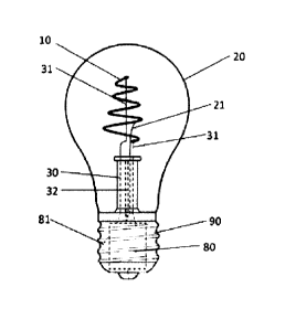
[00112] Figure 14 is a schematic diagram of a bulb with the three-dimensional
LED
encapsulation in the embodiment. The bulb comprises a light-transmitting shell
20, lead wires
31 in the light-transmitting shell, a core column 30 of the core column
exhaust pipe 32 and at
least one the three-dimensional LED encapsulation 10 connecting with the lead
wire 31. Based
on the present disclosure, the electrode wire on the substrate for three-
dimensional LED
encapsulation 10 is connected with electric connector 90 through lead wire 31,
drive 80 and
drive electric lead wire 81, to connect with the external power source to lit
the LED chips. The
light-transmitting shell 20 is connected with the core column 30, forming a
sealed space in the
14
CA 02964421 2017-04-12
light-transmitting shell 20, filled with protective and cooling gas which may
be helium or
hydrogen-helium mixture. The transmitting shell 20 is transparent, milky
white, dull polished, or
color covered, or partially reflective, or covered partly with small prism or
small lens. The
shape of the transmitting bulb shell 20 may be in "A", "G", "R", "PAR", "T"
shapes, candle-like
or in other shapes of existing bulb shells. The electric connector 90 may be
E40, E27, E26,
E14, GU or other existing electric connector. There is a cooling wire 21 in
the light transmitting
bulb 20, wherein the cooling wire 21 connects the core column 30 and the three-
dimensional
LED encapsulation 10 to conduct the heat to core column 30 and to the external
environment.
[00113] The three-dimensional LED encapsulation in the bulb may be a conical
spiral, as
shown in 14, which may be connected to operate AC or DC. When the three-
dimensional LED
encapsulation is operating DC, it may use external DC power or AC power; when
using
external AD power, the drive 80 may be made of a circuit for limiting current
and lowing voltage
with a capacitor and a resistance connected in parallel, and a rectifier and
filter circuit. The
circuit of drive 80 may be simple and low-cost, with no use of electrolytic
capacitor, transistor,
transformer, or high-frequency radiation. It may also be a switcher, a power
source and a
constant current stabilizer.
[00114] The method of making the bulb with three-dimensional LED encapsulation
of the
present disclosure comprises:
[00115] 1) make the three-dimensional LED;
[00116] 2) make a core column 30 with two lead wires 31 and the core column
exhaust pipe
32;
[00117] 3) connect the electrode lead wire 2 of the three-dimensional LED
encapsulation
with the lead wire 31 of the core column 30;
[00118] 4) put the connected three-dimensional LED encapsulation and core
column 30 into
the light-transmitting shell 20, and melt the connective component between the
light-
transmitting shell 20 and core column 30 to fuse the two part as a whole;
[00119] 5) vacuumize the light-transmitting shell 20 using the core column
exhaust pipe 32
and inflate light-transmitting shell 20 with gas that may protect the filament
and promote its
cooling; and then fuse the core column exhaust pipe 32 to form a hermetically
sealed shell;
CA 02964421 2017-04-12
[00120] 6) connect the drive 80 with the electric connector 90 by the electric
lead wire 81,
connect lead wire 31 of the core column with the drive 80, put the drive 80 in
the electric
connector 90 and connect the shell with the electric connector 90;
[00121] The step 1) and step 2) may be implemented in any sequence, or at the
same time.
[00122] Wherein the inflating is to inflate the transmitting shell 20 with gas
that is protective
and hear conductive to the filament.
[00123] Wherein the core column 30 has a cooling wire 21 on it, and the step 3
comprises
connecting the cooling wire 21 with the three-dimensional LED encapsulation
10.
[00124] As shown in Figure 15, another embodiment of the present disclosure is
different
from the bulb above because substrate 1 of the three-dimensional LED
encapsulation in the
bulb is an equal circular spiral and is placed horizontally. And there is a
connective structure
40 between transmitting shell 20 and electric connector 90 which is plastic,
metal, ceramic,
bamboo or rubber. Connective structure 40 may enlarge the neck of the bulb and
place larger
filament or light bar in the bulb, and may enlarge the volume of the shell to
help conduct heat.
[00125] As shown in Figure 16, another embodiment of the present disclosure is
different
from the bulb above because there are two spiral three-dimensional LED
encapsulations 10,
forming a double-spiral. The positions of the two spirals may be opposite,
back-to-back, face-
to-face, or staggered. The number of turns of the two spirals may be the same
or different.
Figures 17a-17d are schematic diagrams of a bulb with the three-dimensional
LED
encapsulation in some embodiments. Figure 17a is a single spiral whose
diameter goes up
along its axial direction. Figure 17b is a double-spiral whose diameter goes
up along its axial
direction. Figure 17c is a single spiral whose diameter goes up and then down
along its axial
direction. Figure 17d is a double-spiral whose diameter goes down and then up
along its axial
direction.
[00126] Figure 18 is schematic diagram of a bulb with the three-dimensional
LED
encapsulation in another embodiment. The bulb comprises a cooling supporter
50, lead wires
31 and at least one spiral three-dimensional LED encapsulation 10, wherein one
lead wire 31
is in the cooling supporter 50 and the two ends of the at least one spiral
three-dimensional
LED encapsulation 10 are connected with a lead wire from cooling supporter 50
and another
lead wire 31 respectively. The transmitting shell and cooling supporter 50 may
be connected
with electric connector 90 directly (not shown in the figure) or through
connective structural
16
CA 02964421 2017-04-12
component 60. Lead wire 31 is connected with drive 80 which is mounted in
connective
structural component 60 and electric connector 90. Connective structural
component 60 may
be plastic, metal, ceramic, bamboo or rubber. Cooling supporter 50 has high
thermal
conductivity and is dielectric (to make electrically neutral thermal path). In
this way, heat may
be conducted from spiral three-dimensional LED encapsulation 10 to connective
structural
component 60. The cooling supporter 50 may be whole formed or form by one or
more
components. the material of each component may be the same, partial same or
different.
[00127] Figure 19 is schematic diagram of a bulb with the three-dimensional
LED
encapsulation 10 in another embodiment. The bulb in this embodiment is much
similar with
that in Figure 18. The difference is, cooling supporter 50 does not touch the
three-dimensional
LED encapsulation; and the three-dimensional LED encapsulation 10 is supported
by lead
wires 31. In this way, two lead wires 31 support the three-dimensional LED
encapsulation 10
and conduct heat and electricity. The lead wires conduct heat from three-
dimensional LED
encapsulation to cooling supporter 50 and connective structural component 60.
[00128] Based on bulbs in Figures 18 and 19, the structures are formed only by
the
transmitting shell, lead wires and the electric connector. Because the cooling
supporter and
two lead wires 31 may conduct heat well, there is no need to seal, vacuumize
and fuse the
bulbs.
[00129] The method for bulbs with three-dimensional LED encapsulation in
Figures 18 and
19 comprises:
[00130] 1) make the three-dimensional LED encapsulation;
[00131] 2) prepare a cooling supporter 50 with two lead wires 31;
[00132] 3) connect the electrode lead wire 2 of the three-dimensional LED
encapsulation
with the lead wire 31;
[00133] 4) put the connected three-dimensional LED encapsulation and cooling
supporter 50
into the light-transmitting shell 20, and connect and fix the light-
transmitting shell 20 and the
cooling supporter 50;
[00134] 5) connect the drive 80 with the electric connector 90 by the electric
lead wire (81)
and connect lead wire 31 of the core column with the drive 80;
[00135] 6) put the drive 80 in the electric connector 90 and connect the
cooling supporter 50
with the electric connector 90 directly or through connective components 60;
17
CA 02964421 2017-04-12
[00136] Wherein the step 1) and step 2) may be implemented in any sequence, or
at the
same time.
[00137] Wherein cooling supporter 50 has high thermal conductivity and is
dielectric to make
electrically neutral thermal path, like APL.
[00138] The connective structural component 60 is made or plastic, metal,
ceramic, bamboo
or rubber.
[00139] Wherein the three-dimensional LED encapsulation is fixedly connected
with the
cooling supporter 50, and may support the three-dimensional LED encapsulation
with cooling
supporter 50; or the cooling supporter 50 does not touch the three-dimensional
LED
encapsulation and the three-dimensional LED encapsulation is supported by lead
wires 31.
[00140] The cooling supporter 50 may be in one piece, or made of more than one
component as described above.
[00141] According to the present disclosure, the bulb may be all-directional,
three-
dimensional, and multi-layer glowing. The bulb is also heat conductive, large
in glowing angle,
and uniform in light intensity. In addition, the manufacturing process is
simple, convenient, and
low-cost.
18