Note: Descriptions are shown in the official language in which they were submitted.
CA 02964802 2017-04-13
WO 2016/064727 PCT/US2015/056206
DIGITAL POWER RECEIVER SYSTEM
BACKGROUND
Digital electric power, or digital electricity, can be characterized as any
power
format where electrical power is distributed in discrete, controllable units
of energy.
Packet energy transfer (PET) is a new type of digital electric power protocol
disclosed
in U.S. Pat. No. 8,781,637 (Eaves 2012).
The primary discerning factor in a digital power transmission system
comparcd to traditional, analog powcr systcms is that thc electrical cncrgy is
separated into discrete units; and individual units of energy can be
associated with
analog and/or digital information that can be used for the purposes of
optimizing
safety, efficiency, resiliency, control or routing.
As described by Eaves 2012, a source controller and a load controller are
connected by power transmission lines. The source controller of Eaves 2012
periodically isolates (disconnects) the power transmission lines from the
power
source and analyzes, at a minimum, the voltage characteristics present at the
source
controller terminals directly before and after the lines are isolated. The
time period
when the power lines are isolated was referred to by Eaves 2012 as the "sample
period", and the time period when the source is connected is referred to as
the
"transfer period". The rate of rise and decay of the voltage on the lines
before,
during and after the sample period reveal if a fault condition is present on
the power
transmission lines. Measurable faults include, but are not limited to, short
circuit,
high line resistance or the presence of an individual who has improperly come
in
contact with the lines.
Eaves 2012 also describes digital information that may be sent between the
source and load controllers over the power transmission lines to further
enhance
safety or provide general characteristics of the energy transfer, such as
total energy
or the voltage at thc load controller terminals. Sincc thc cncrgy in a PET
systcm is
transferred as discrete quantities, or quanta, it can be referred to as
"digital power"
or "digital electricity".
One application of a digital power distribution system is to distribute direct-
current (DC) power in digital format and at elevated voltage from the source
side of
1
CA 02964802 2017-04-13
WO 2016/064727 PCT/US2015/056206
the system to the load side. At the load side of the power distribution
system, the DC
power is converted from digital format back to traditional analog DC format,
using a
circuit referred to as a receiver, for use in commonly available power
conditioning
circuits. Power conditioning circuits, widely known to the industry, take an
input
voltage and produce a controlled alternating-current (AC) or DC output
voltage.
One example is a conditioner that takes a 380V DC input and creates a 12V DC
output for use in a computer. A power conditioning circuit can also convert a
DC
input to an AC output, as is commonly found in unintcrruptablc powcr supplies
or
inverters. In its most basic form, a power conditioner is a simple switch that
either
allows or inhibits current flow.
SUMMARY
A digital power receiver system and a method for regulating digital power are
described herein, where various embodiments of the apparatus and methods may
include some or all of the elements, features and steps described below.
A digital power receiver system supplied by a digital power distribution
system, comprises one or more individual receiver circuits that are each
connected
to an individual transmission line pair originating from a digital power
transmission
source and where the one or more individual receiver circuits are configured
to
convert thc digital powcr on thc transmission line pair to analog power; onc
or morc
receiver output bus segments that electrically connect groups of the one or
more
individual receiver circuits in parallel; one or more power conditioning
circuits
configured to connect to the one or more individual receiver circuits or to
the one or
more receiver output bus segments; one or more power conditioning circuit
output
bus segments that electrically connect the output terminals of the one or more
power
conditioning circuits to provide a combined power output; and a control
circuit that
is operable to monitor at least one voltage within the digital power receiver
system
and to act to regulate output power of at least one power conditioning circuit
to
improve at least one of safety, efficiency, resiliency, control and routing of
power.
A method for regulating digital power comprises transmitting digital power
via a transmission line pair to at least one receiver circuit in a digital
power receiving
system; converting the digital power into analog power in the receiver
circuit;
2
CA 02964802 2017-04-13
WO 2016/064727
PCT/US2015/056206
transmitting the analog power to at least one power conditioning circuit;
transmitting output power from the power conditioning circuit; monitoring at
least
one voltage in the digital power receiver system; and in response to that
monitoring,
regulating the output power from the power conditioning circuit to improve at
least
one of safety, efficiency, resiliency, control, and routing of power.
BRIEF DESCRIPTION OF THE DRAWINGS
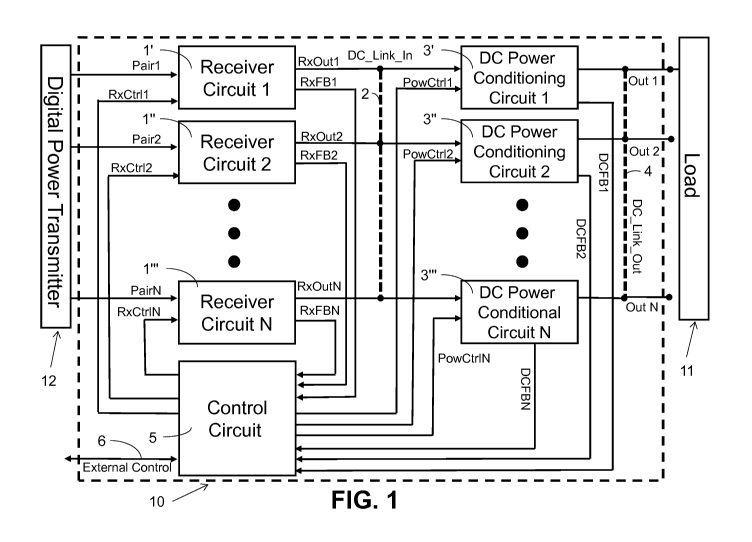
FIG. 1 is a block diagram of a digital power receiving system.
FIG. 2 is a block diagram of an cmbodimcnt of a receiver circuit.
FIG. 3 is a block diagram of an embodiment of a receiver circuit including a
switch in the form of a simple diode 20.
FIG. 4 is a block diagram of an embodiment of a DC power conditioning
circuit.
In the accompanying drawings, like reference characters refer to the same or
similar parts throughout the different views; and apostrophes are used to
differentiate multiple instances of the same or similar items sharing the same
reference numeral. The drawings are not necessarily to scale; instead, an
emphasis is
placed upon illustrating particular principles in the exemplifications
discussed
below.
DETAILED DESCRIPTION
The foregoing and other features and advantages of various aspects of the
invention(s) will be apparent from the following, more-particular description
of
various concepts and specific embodiments within the broader bounds of the
invention(s). Various aspects of the subject matter introduced above and
discussed
in greater detail below may be implemented in any of numerous ways, as the
subject
matter is not limited to any particular manner of implementation. Examples of
specific implementations and applications are provided primarily for
illustrative
purposes.
Unless otherwise herein defined, used or characterized, terms that are used
herein (including technical and scientific terms) are to be interpreted as
having a
meaning that is consistent with their accepted meaning in the context of the
relevant
3
CA 02964802 2017-04-13
WO 2016/064727 PCT/US2015/056206
art and are not to be interpreted in an idealized or overly formal sense
unless
expressly so defined herein. For example, if a particular composition is
referenced,
the composition may be substantially (though not perfectly) pure, as practical
and
imperfect realities may apply; e.g., the potential presence of at least trace
impurities
(e.g., at less than 1 or 2%) can be understood as being within the scope of
the
description. Likewise, if a particular shape is referenced, the shape is
intended to
include imperfect variations from ideal shapes, e.g., due to manufacturing
tolerances. Pcrccntagcs or conccntrations expressed hcrcin can bc in tcrms of
wcight
or volume. Processes, procedures and phenomena described below can occur at
ambient pressure (e.g., about 50-120 kPa¨for example, about 90-110 kPa) and
temperature (e.g., -20 to 50 C¨for example, about 10-35 C) unless otherwise
specified.
Although the terms, first, second, third, etc., may be used herein to describe
various elements, these elements are not to be limited by these terms. These
terms
are simply used to distinguish one element from another. Thus, a first
element,
discussed below, could be termed a second element without departing from the
teachings of the exemplary embodiments.
Spatially relative terms, such as "above," "below," "left," "right," "in
front,"
"behind," and the like, may be used herein for ease of description to describe
the
relationship of one element to another element, as illustrated in the figures.
It will be
understood that the spatially relative terms, as well as the illustrated
configurations,
are intended to encompass different orientations of the apparatus in use or
operation in addition to the orientations described herein and depicted in the
figures. For example, if the apparatus in the figures is turned over, elements
described as "below" or "beneath" other elements or features would then be
oriented
"above" the other elements or features. Thus, the exemplary term, "above," may
cncompass both an oricntation of above and below. Thc apparatus may bc
othcrwisc
oriented (e.g., rotated 90 degrees or at other orientations) and the spatially
relative
descriptors used herein interpreted accordingly.
Further still, in this disclosure, when an element is referred to as being
"on,"
"connected to," "coupled to," "in contact with," etc., another element, it may
be
4
CA 02964802 2017-04-13
WO 2016/064727 PCT/US2015/056206
directly on, connected to, coupled to, or in contact with the other element or
intervening elements may be present unless otherwise specified.
The terminology used herein is for the purpose of describing particular
embodiments and is not intended to be limiting of exemplary embodiments. As
used
herein, singular forms, such as "a" and "an," are intended to include the
plural forms
as well, unless the context indicates otherwise. Additionally, the terms,
"includes,"
"including," "comprises" and "comprising," specify the presence of the stated
elements or stcps but do not preclude thc prcscncc or addition of onc or morc
othcr
elements or steps.
Additionally, the various components identified herein can be provided in an
assembled and finished form; or some or all of the components can be packaged
together and marketed as a kit with instructions (e.g., in written, video or
audio
form) for assembly and/or modification by a customer to produce a finished
product.
Morc specifically, disclosed hcrcin is a novel combination of traditional
powcr
conditioning circuitry and digital power receiver circuits that can improve or
optimize factors of safety, efficiency, resiliency, control and routing of
power, and
that can prioritize digital power delivery across multiple loads based on a
predetermined priority scheme.
In many cases, to support higher power levels or to offer redundancy, multiple
transmission pairs are combined in parallel. One difficulty that arises when
power-
limited circuits are combined in parallel is that the individual circuits do
not always
share the total load equally due to minor variances in circuit impedance.
Reasons for
variances in circuit impedance may include differences in transmission pair
cross-
sectional diameter at the same length and/or differences in transmission pair
lengths.
A second difficulty is the proper synchronization of the circuits during start-
up. For example, consider a two circuit system that must power a total of 200W
but
where any individual circuit is power limited to 100W. If one of the two
circuits
starts up before the other, it will momentarily need to support all of the
load
requirements (i.c., 200W). This load exceeds the circuit's 100W maximum
capacity,
5
CA 02964802 2017-04-13
WO 2016/064727 PCT/US2015/056206
resulting in a shut-down of the circuit due to the over-power, non-compliant
condition. Circuits configured to automatically reset would typically wait
from 1 to
60 seconds before retrying the power-up sequence. While the first circuit is
waiting to
retry, the second circuit will come on-line and, in turn, try to support the
entire
200W load and, in turn, shut down because of the over-power, non-compliant
condition. If there is no synchronization of the digital power circuits, the
faulty start-
up sequence may continue indefinitely.
Yct a third difficulty ariscs whcn rcsponding to thc failure of an individual
circuit that is part of a larger parallel group. In many instances, the
circuits are
supplying loads that have priority levels associated with them. For example, a
supply
circuit that is powering a heart pump should have priority over one that is
supplying
general lighting in a hospital. When an individual circuit fails, it would be
advantageous to have a prearranged prioritization scheme that would determine
which loads will receive a reduced allocation of power. Moreover, the
prioritization
scheme would ideally be configurable by an outside host system. One method to
allow an outside host system to configure the prioritization scheme is through
the
implementation of what is commonly known in the industry as an Application
Programming Interface (API).
Disclosed herein is an architecture that can address the above-discussed
difficulties economically and reliably and that can support a wide range of
parallel
digital power circuits ranging from one to dozens in parallel. Additionally,
as will be
described below, the communications features of the PET protocol described in
Eaves 2012 are leveraged to implement optimized combinations of safety,
efficiency,
resiliency, control or routing, and to allow priority levels to be set on the
delivery of
power to multiple loads.
A block diagram of a digital power receiver system 10 is shown in FIG. 1. This
systcm includes a digital powcr receiver configurcd to operatc with packct
cncrgy
transfer (PET) protocol. Packet energy transfer and, more specifically, the
transmitter source of power is described in Eaves 2012. One or more receiver
circuits
1 each have a transmission line pair (Pairl, Pair2, PairN) originating from
the PET
transmission source 12. Individual receiver circuit outputs can be combined in
6
CA 02964802 2017-04-13
WO 2016/064727 PCT/US2015/056206
parallel on electrical receiver output bus (DC_Link_In) 2. The DC input
terminals of
one or more DC power conditioning circuits 3 are tied to available segments of
DC_Link_In 2. The individual outputs of the power conditioning circuits 3 can
be
combined in parallel or operated separately by connecting or disconnecting
segments of the power conditioning circuit output bus (DC_Link_Out) 4. The
operation of the receiver circuits 1 and power conditioning circuits 3 is
managed by
control circuit 5. The control circuit 5 obtains feedback on the operation of
the
receiver and powcr conditioning circuits 1 and 3 through fccdback line groups,
RxFB1, RxFB2, RxFBN, DCFB1, DCFB2, DCFBN. The control circuit 5 is analogous
to the load controller described in Eaves 2012 with the difference being that
it
manages multiple transmission line pairs versus only one pair in Eaves 2012.
The
control circuit 5 can be a fully functional processor executing the necessary
algorithms to prioritize the allocation of energy to the various power
conditioning
circuits 3 and optimizing safety, efficiency, resiliency, control and routing.
In other
embodiments, the control circuit 5 can be a simplified version executing
commands
for operation originating from a remote processing device.
Overall, control circuit 5 can monitor the availability of power from each
receiver circuit 1 to determine if, how many, and at what power level each of
the DC
power conditioning circuits 3 will be operated. As discussed in the background
section, for operation of parallel connected groups, multiple receiver
circuits 1 are
synchronously activated to deliver power, or one or more of the receiver
channels
can overload as the load devices 11 attached to the DC power conditioning
circuit 1
outputs begin drawing power. Control circuit 5 can control the rate of power
transfer in each of the power conditioning circuits 3 through control line
groups,
including a first power controller (PowCtr11), a second power controller
(PowCtr12),
up to an Nth power controller (PowCtr1N).
An cmbodimcnt of a receiver circuit 1 is shown in FIG. 2. Switch SW1 20
controls electrical current flow into the receiver circuit 1. SW1 20 can be in
the form
of controllable switches (electro-mechanical or solid-state electronic) as
shown in
FIG. 2; or it may be a simple diode as depicted in FIG. 3. The receiver
circuits 1
convert the digital power on the conductor pair back to conventional analog
7
CA 02964802 2017-04-13
WO 2016/064727 PCT/US2015/056206
electricity that no longer comprises discrete units or pulses. This conversion
is
performed by rectification, either actively (using a controllable switch) or
passively
(using a diode). The rectification is performed by SW1 20, which inhibits
current
flow from a receiver DC link 22 back into the receiver conductor pair when the
digital power source 12, or transmitter, terminates an energy pulse. The
transmitter
12 terminates the energy pulse by opening its own switch (making the switch
non-
conducting) on the transmitter side of the system. At this point the
transmission
pairs arc electrically isolated from both thc transmittcr and thc receiver,
allowing at
a minimum, the transmitter 12 to analyze the receiver conductor pair to
determine if
the voltage decay is within predetermined parameters, as described in Eaves
2012.
SW1 20 can comprise a bi-directional switch that can control current flow in
either direction. The receiver circuits 1 can then be combined with bi-
directional
power conditioning circuits 3. This allows power to flow in reverse from the
output
of the power conditioning circuits 3, back through the receiver circuits 1 and
into the
transmission line pairs. This ability is useful in cases where the load 11 can
reverse
roles and become a source of energy. For example, where the digital power
receiver
system 10 is feeding a home at night, the home can have photovoltaic solar
panels
that provide an excess of power that can be sent back through the digital
power
receiver system 10 to be sold back to the utility. In another embodiment, an
energy
storage device, such as a battery, is positioned to receive the output of one
or more
of the power conditioning circuits 3. The battery can be charged at one
instance, but
then can be later discharged back into the digital power receiver system 10.
The
digital power receiver system 10 can execute a routing algorithm where a
portion of
the energy in the energy storage device is sent via the transmission lines
back to the
transmission source 12, and the remainder of the energy from the storage
device is
distributed according to a priority scheme to the various power conditioning
circuits
3', 3", and 3" in thc systcm 10.
The control circuit 5 can send communications signals via the receiver control
line group, RxCtr11 RxCtr12, RxCtr1N, to the receiver modulation circuit 23 of
FIG. 2.
The modulation circuit 23, using techniques commonly known to the industry,
can
superimpose and modulate a communication signal on the transmission line pair,
8
CA 02964802 2017-04-13
WO 2016/064727 PCT/US2015/056206
PairN. The modulated signal can, in turn, be demodulated at the corresponding
transmitter source controller, as detailed in Eaves 2012. The transmitter
source
controller can then be instructed to turn on, turn off, or set limits on the
output
power, voltage or current available on the transmission line pair.
An example for the use of the communications capability is where the control
circuit 5 communicates back to each of the transmitter source controllers;
notifying
them that they are all providing power to the same digital power receiver
system 10.
In this way, thc individual transmittcr controllers can act to balance power
flow to
all of the involved transmission line pairs or, according to a preconfigured
prioritization scheme, allow a higher power limit to one pair versus another.
A
further example is where a receiver controller acquires a receiver circuit
voltage,
such as at point 18 of FIG. 2, or power conditioning circuit voltage, such as
at point
27 of FIG. 4, and communicates the value to one or more transmitter
controllers.
The controllers then adjust their average output to regulate the voltage at
the
receiver according to a predetermined set point. The receiver controller can
accomplish a similar result by periodically sending a command to the
transmitter
controllers that direct the controllers to increase or decrease their average
output
voltage in order to maintain a predetermined voltage set point at the
receiver.
Among other methods, average output voltage variation can be achieved by
adjusting the duty cycle of the transfer period versus sample period of the
PET
waveform, as described in Eaves 2012.
Without communicating back to the corresponding transmitter controllers,
the control circuit 5 has the capability to sense if a receiver circuit 1 is
ready to
deliver power by acquiring the voltage at the receiver input at point 18 of
FIG. 2 and
determining if it has reached a predetermined minimum value. The controller
can
wait until a minimum number of receiver circuits 1', 1", and/or 1' are ready
to
deliver powcr bcforc enabling onc or morc powcr conditioning circuits 3', 3",
and/or
3" via the control line groups, PowCtr11, PowCtr12, PowCtr1N. Alternatively,
if only a
limited number of receiver circuits 1', 1", and/or 1' are ready to deliver
power, the
control circuit 5 can be configured to distribute the available power to the
power
conditioning circuits 3', 3", and/or 3" according to a prearranged
prioritization
9
CA 02964802 2017-04-13
WO 2016/064727 PCT/US2015/056206
scheme. In this case, DC_Link_Out 4, shown as the dotted line in FIG. 1, is
removed
from at least one of the power conditioning circuits 3', 3", and/or 3" to
allow the
power conditioning circuit 373"/3" to deliver power to a load 11 individually.
The
prioritization scheme can be locally programmed in the controller or can be
programmed remotely from the transmitter controllers via the modulation
circuits
in the receiver circuits 1.
Yet another method to allocate available power from the receiver circuits 1 to
thc powcr conditioning circuits 3 is to mcasurc voltage and/or currcnt at
individual
power conditioning circuits 3', 3", and 3' via DC feedback line groups, DCFB1,
DCFB2, DCFBN, and limit the amount of power or energy that can be provided by
a
power conditioning circuit 3 based on the prioritization scheme using power
conditioner control line groups, PowCtr11, PowCtr12, PowCtr1N. For example, DC
power conditioning circuit 3', 3", or 3' can be supplying a heart pump charger
and
is enabled as soon as the minimum number of receiver circuits 1', 1", and/or
1" for
its individual load requirement are satisfied and before any other power
conditioning circuit 3', 3", or 3" is enabled. One should note that there may
be
different settings for the minimum number of available receiver circuits 1 for
enabling a power conditioning circuit 3 versus disabling a power conditioning
circuit 3, including allowing operation of power conditioning circuits 3 as
long as
just one receiver circuit 1', 1", or 1' is available to deliver power. An
additional
example is the case where a conductor pair can be configured to support an
initially
high current for a device with high in-rush current requirements but would
later be
configured to limit current to a lower level for the most efficient operation.
In the embodiment of the DC power conditioning circuit 3 depicted in FIG. 4,
a second switch (SW2) 24 and a third switch (SW3) 25 comprise transistor
switches.
In this case, control circuit 5 keeps SW2 24 and SW3 25 in an open (non-
conducting
state) until thc receiver input voltages, as provided by RxFB1, RxFB2, RxFBN,
rcach
a minimum value that indicates that the receiver channels are fully
initialized and
ready to deliver power. When a minimum number of receiver circuits 1 are ready
to
provide power, the control circuit 5 will act to close (place into a
conducting state)
SW3 25. SW3 25 connects the receiver circuits 1 to the output of the DC power
CA 02964802 2017-04-13
WO 2016/064727 PCT/US2015/056206
conditioning circuit 3 through a series resistor, R1 26. R1 26 limits the
current flow
when charging the input capacitance that can be part of a load device 11
attached to
the output bus, DC_Link_Out 4. The action of R1 26 and SVV2 24 are commonly
referred to in the industry as a pre-charge circuit. After the pre-charge time
has
expired, a direct connection to the load device 11 is made by closing the
second
switch, SW2 24 and then opening the third switch, SW3 25. Thus, the receiver
circuits 1 are simultaneously engaged and able to provide a substantial pulse
power
capability.
Referring back to FIG. 1, the external control channel 6 allows additional
sensor signals or communication signals from an external device to be acquired
by
the control circuit 5. For example, the external control channel 6 can include
an
external temperature sensor, an ambient light sensor, or a serial
communications
stream. The external controlchannel 6 can be offered as a third-party
interface. For
example, the digital power receiver system 10 can be part of a LED lighting
fixture;
and the manufacture of the fixture may wish to send data on ambient light
conditions back over the transmission line pairs to the transmission source 12
and
may also wish to send control signals out though external control channel 6 to
set
the dimming level of the LED fixture. External control channel 6 can also be
connected to a corresponding "communication link" in the transmission source
controller, as described in Eaves 2012. This connection can avoid the
necessity to
communicate to the transmitter source controller via modulation of the
transmission line pairs, as described above.
In describing embodiments of the invention, specific terminology is used for
the sake of clarity. For the purpose of description, specific terms are
intended to at
least include technical and functional equivalents that operate in a similar
manner
to accomplish a similar result. Additionally, in some instances where a
particular
cmbodimcnt of thc invention includes a plurality of systcm elements or mcthod
steps, those elements or steps may be replaced with a single element or step;
likewise,
a single element or step may be replaced with a plurality of elements or steps
that
serve the same purpose. Further, where parameters for various properties or
other
values are specified herein for embodiments of the invention, those parameters
or
11
WO 2016/064727 PCT/US2015/056206
values can be adjusted up or down by 1/100th, 1/50th, 1/20th, 1/10th, 1/5th,
1/3rd,
1/2, 2/3rd, 3/4th, 4/5th, 9/10th, 19/20th, 49/50th, 99/100th, etc. (or up by a
factor of
1, 2, 3, 4, 5, 6, 8, 10, 20, 50, 100, etc.), or by rounded-off approximations
thcrcof,
unless otherwise specified. Moreover, while this invention has been shown and
dcscribcd with references to particular embodiments thereof, those skilled in
the art
will undcrstand that various substitutions and alterations in form and details
may be
made therein without departing from the scope of the invention. Further still,
other
aspects, functions and advantages are also within the scope of the invention;
and all
embodiments of the invention need not necessarily achieve all of the
advantages or
posscss all of the characteristics described above. Additionally, steps,
elements and
features discussed herein in connection with one embodiment can likewise be
used
in conjunction with other embodiments. The contcnts of references, including
reference tcxts, journal articles, patents, patent applications, etc.,
and appropriate
components, steps, and characterizations from these references may or may not
be
included in embodiments of this invention. Still further, the components and
steps
identified in the Background section are integral to this disclosure and can
be used
in conjunction with or substituted for components and steps described
elsewhere in
the disclosure within the scope of the invention. In method claims, where
stages are
recited in a particular order¨with or without sequenced prefacing characters
added
for ease of reference¨the stages are not to be interpreted as being temporally
limited to the ordcr in which they arc rccitcd unless othcrwisc spccificd or
implied
by the terms and phrasing.
12
CA 2964802 2017-10-27