Note: Descriptions are shown in the official language in which they were submitted.
CA 02965870 2017-04-25
WO 2016/073522 PCT/US2015/058890
ENERGY STORAGE DEVICES AND METHODS OF PRODUCTION THEREOF
BACKGROUND
[0001] A capacitor is a passive electronic component that is used to store
energy in the form of an
electrostatic field, and comprises a pair of electrodes separated by a
dielectric layer. When a
potential difference exists between two electrodes, an electric field is
present in the dielectric layer.
This field stores energy and an ideal capacitor is characterized by a single
constant value of
capacitance which is a ratio of the electric charge on each electrode to the
potential difference
between them. In practice, the dielectric layer between electrodes passes a
small amount of leakage
current. Electrodes and leads introduce an equivalent series resistance, and
dielectric layer has
limitation to an electric field strength which results in a breakdown voltage.
The simplest capacitor
consists of two parallel electrodes separated by a dielectric layer of
permittivity c, each of the
electrodes has an area S and is placed on a distance d from each other.
Electrodes are considered to
extend uniformly over an area S. and a surface charge density can be expressed
by the equation: +I)
= Q/S. As the width of the electrodes is much greater than the separation
(distance) d, an electrical
field near the centre of the capacitor will be uniform with the magnitude E =
p/c. Voltage is defined
as a line integral of the electric field between electrodes. An ideal
capacitor is characterized by a
constant capacitance C defined by the formula (1)
C = Q/V, (1)
which shows that capacitance increases with area and decreases with distance.
Therefore the
capacitance is largest in devices made of materials of high permittivity.
[0002] A characteristic electric field known as the breakdown strength Ebd, is
an electric field in
which the dielectric layer in a capacitor becomes conductive. Voltage at which
this occurs is called
the breakdown voltage of the device, and is given by the product of dielectric
strength and separation
between the electrodes,
Vbd = Ebdd (2)
[0003] The maximal volumetric energy density stored in the capacitor is
limited by the value
proportional to ¨c=E2bd, where 8 is dielectric permittivity and Ebd is
breakdown strength. Thus,
in order to increase the stored energy of the capacitor it is necessary to
increase dielectric
permeability c and breakdown strength Ebd of the dielectric.
-1-
CA 02965870 2017-04-25
WO 2016/073522 PCMJS2015/058890
[0004] For high voltage applications much larger capacitors have to be used.
There are a number of
factors that can dramatically reduce the breakdown voltage. Geometry of the
conductive electrodes
is important for these applications. In particular, sharp edges or points
hugely increase the electric
field strength locally and can lead to a local breakdown. Once a local
breakdown starts at any point,
the breakdown will quickly "trace" through the dielectric layer till it
reaches the opposite electrode
and causes a short circuit.
[0005] Breakdown of the dielectric layer usually occurs as follows. Intensity
of an electric field
becomes high enough free electrons from atoms of the dielectric material and
make them conduct an
electric current from one electrode to another. Presence of impurities in the
dielectric or
imperfections of the crystal structure can result in an avalanche breakdown as
observed in
semiconductor devices.
[0006] Other important characteristic of a dielectric material is its
dielectric permittivity. Different
types of dielectric materials are used for capacitors and include ceramics,
polymer film, paper, and
electrolytic capacitors of different kinds. The most widely used polymer film
materials are
polypropylene and polyester. Increase of dielectric permittivity allows
increasing of volumetric
energy density which makes it an important technical task.
[0007] An ultra-high dielectric constant composite of polyaniline,
PANI¨DBSA/PAA, was
synthesized using in situ polymerization of aniline in an aqueous dispersion
of poly-acrylic acid
(PAA) in the presence of dodecylbenzene sulfonate (DBSA) (see, Chao-Hsien Hoa
et al., "High
dielectric constant polyaniline/poly(acrylic acid) composites prepared by in
situ polymerization",
Synthetic Metals 158 (2008), pp. 630-637). The water-soluble PAA served as a
polymeric
stabilizer, protecting the PANI particles from macroscopic aggregation. A very
high dielectric
constant of ca. 2.0*105 (at 1 kHz) was obtained for the composite containing
30% PANI by weight.
Influence of the PANI content on the morphological, dielectric and electrical
properties of the
composites was investigated. Frequency dependence of dielectric permittivity,
dielectric loss, loss
tangent and electric modulus were analyzed in the frequency range from 0.5 kHz
to 10 MHz. SEM
micrograph revealed that composites with high PANI content (i.e., 20 wt.%)
consisted of numerous
nano-scale PANI particles that were evenly distributed within the PAA matrix.
High dielectric
constants were attributed to the sum of the small capacitors of the PANI
particles. The drawback of
this material is a possible occurrence of percolation and formation of at
least one continuous
conductive path under electric field with probability of such an event
increasing with an increase of
the electric field. When at least one continuous path (track) through the
neighboring conducting
-2-
CA 02965870 2017-04-25
WO 2016/073522 PCMJS2015/058890
PAN1 particles is formed between electrodes of the capacitor, it decreases a
breakdown voltage of
such capacitor.
[0008] Colloidal polyaniline particles stabilized with a water-soluble
polymer, poly(N-
vinylpyrrolidone) [poly(1-vinylpyrrolidin-2-one)J, have been prepared by
dispersion polymerization.
The average particle size, 241 50 nm, have been determined by dynamic light
scattering (see,
Jaroslav Stejskal and Irina Sapurina, "Polyaniline: Thin Films and Colloidal
Dispersions (IUPAC
Technical Report)", Pure and Applied Chemistry, Vol. 77, No. 5, pp. 815-826
(2005).
[0009] Single crystals of doped aniline oligomers are produced via a simple
solution-based self-
assembly method (see, Yue Wang, et. al., "Morphological and Dimensional
Control via Hierarchical
Assembly of Doped Oligoaniline Single Crystals", J. Am. Chem. Soc. 2012,134,
pp. 9251-9262).
Detailed mechanistic studies reveal that crystals of different morphologies
and dimensions can be
produced by a "bottom-up" hierarchical assembly where structures such as one-
dimensional (1-D)
nano fibers can be aggregated into higher order architectures. A large variety
of crystalline
nanostructures, including 1-D nano fibers and nanowires, 2-D nanoribbons and
nanosheets, 3-D
nanoplates, stacked sheets, nanoflowers, porous networks, hollow spheres, and
twisted coils, can be
obtained by controlling the nucleation of the crystals and the non-covalent
interactions between the
doped oligomers. These nanoscale crystals exhibit enhanced conductivity
compared to their bulk
counterparts as well as interesting structure-property relationships such as
shape-dependent
crystallinity. Furthermore, the morphology and dimension of these structures
can be largely
rationalized and predicted by monitoring molecule-solvent interactions via
absorption studies. Using
doped tetra-aniline as a model system, the results and strategies presented in
this article provide
insight into the general scheme of shape and size control for organic
materials.
[0010] There is a known energy storage device (capacitor) based on a
multilayer structure. The
energy storage device includes first and second electrodes, and a multilayer
structure comprising
blocking and dielectric layers. The first blocking layer is disposed between
the first electrode and a
dielectric layer, and the second blocking layer is disposed between the second
electrode and a
dielectric layer. Dielectric constants of the first and second blocking layers
are both independently
greater than the dielectric constant of the dielectric layer. A drawback of
this device is that blocking
layers of high dielectric permittivity located directly in contact with
electrodes can lead to
destruction of the energy storage device. Materials with high dielectric
permittivity which are based
on composite materials and containing polarized particles (such as PANI
particles) may demonstrate
a percolation phenomenon. The formed polycrystalline structure of layers has
multiple tangling
-3-
CA 02965870 2017-04-25
WO 2016/073522 PCT/US2015/058890
chemical bonds on borders between crystallites. When the used material with
high dielectric
permittivity possesses polycrystalline structure, a percolation may occur
along the borders of crystal
grains. Another drawback of the known device is an expensive manufacturing
procedure which is
vacuum deposition of all layers.
[0011] Capacitors as energy storage device have well-known advantages versus
electrochemical
energy storage, e.g. a battery. Compared to batteries, capacitors arc able to
store energy with very
high power density, i.e. charge/recharge rates, have long shelf life with
little degradation, and can be
charged and discharged (cycled) hundreds of thousands or millions of times.
However, capacitors
often do not store energy in small volume or weight as in case of a battery,
or at low energy storage
cost, which makes capacitors impractical for some applications, for example
electric vehicles.
Accordingly, it may be an advance in energy storage technology to provide
capacitors of higher
volumetric and mass energy storage density and lower cost.
SUMMARY
[0012] The present disclosure provides energy storage devices (e.g.,
capacitors) and methods of
production thereof Energy storage devices of the present disclosure may solve
a problem of the
further increase of volumetric and mass density of reserved energy associated
with some energy
storage devices, and at the same time reduce cost of materials and
manufacturing process.
[0013] In an aspect, a capacitor comprises a first electrode, a second
electrode, and a solid multilayer
structure disposed between said first and second electrodes. Said electrodes
are planar and positioned
parallel to each other, and said solid multilayer structure comprises layers
disposed parallel to said
electrodes and has following sequence: (A-B)õ-A, where A is an insulating
layer; B is a polarization
layer comprising a micro-dispersion of electro-conductive nano-particles in an
insulator matrix, and
number in > 1. In some situations, in can be greater than or equal to 1, 2, 3,
4, 5, 6, 7, 8, 9, 10, 20,
30, 40, 50, 100, 200, 300, 400, 500, or 1000. In some examples, in is from 1
to 1000, 1 to 100, or 1
to 50. The electrodes can be nearly or substantially parallel to each other.
The electrodes can be off-
set from a parallel configuration.
[0014] In another aspect, a method of producing a capacitor comprises (a)
preparation of a
conducting substrate serving as one of the electrodes, (b) formation of a
solid multilayer structure,
and (c) formation of the second electrode on the multilayer structure, wherein
formation of the
multilayer structure comprises alternating steps of the application of
insulating and polarization
layers or a step of coextrusion of the layers.
-4-
[0015] In another aspect, a method of producing a capacitor comprises coating
of insulating layers
on both electrodes, and coating of a multilayer structure on one of electrodes
with lamination of
second electrode to multilayer structure.
[0016] Additional aspects and advantages of the present disclosure will become
readily apparent to
those skilled in this art from the following detailed description, wherein
only illustrative
embodiments of the present disclosure are shown and described. As will be
realized, the present
disclosure is capable of other and different embodiments, and its several
details are capable of
modifications in various obvious respects, all without departing from the
disclosure. Accordingly,
the drawings and description are to be regarded as illustrative in nature, and
not as restrictive.
[0017]
BRIEF DESCRIPTION OF THE DRAWINGS
[0018] The novel features of the invention are set forth with particularity in
the appended claims. A
better understanding of the features and advantages of the present invention
will be obtained by
reference to the following detailed description that sets forth illustrative
embodiments, in which the
principles of the invention are utilized, and the accompanying drawings of
which:
[0019] Figure 1 schematically shows an energy storage device, in accordance
with some
embodiments of the present disclosure; and
[0020] Figure 2 schematically shows another energy storage device, in
accordance with some
embodiments of the present disclosure.
DETAILED DESCRIPTION
[0021] While various embodiments of the invention have been shown and
described herein, it will
be obvious to those skilled in the art that such embodiments are provided by
way of example only.
Numerous variations, changes, and substitutions may occur to those skilled in
the art without
departing from the invention. It should be understood that various
alternatives to the embodiments
of the invention described herein may be employed.
[0022] The present disclosure provides energy storage devices, such as
capacitors. In one
embodiment of the present invention, the insulating layers are crystalline.
The insulating layers can
-5-
Date recue / Date received 2021-12-10
CA 02965870 2017-04-25
WO 2016/073522 PCMJS2015/058890
be fabricated from any suitable crystalline material including a single
crystal material, a batch crystal
material, or amorphous material. Depending on the application, dielectric
permittivity of the
insulating dielectric material Eins may be in the broad range. The insulating
layer comprises a
material characterized by a band gap of greater than 4 eV and by breakdown
field strength of greater
than about 0.001 volts (V)/nanometer (nm), 0.01 V/nm, 0.05 V/nm, 0.1 V/nm, 0.2
V/nm, 0.3 V/nm,
0.4 V/nm, 0.5 V/nm, 1 V/nm, or 10 V/nm. The material of the polarization
layers possesses
dielectric permittivity Epo which may be in the broad range. In some cases,
Epoi is at least about 100,
200, 300, 400, 500, 1000, 2000, 3000, 4000, 5000, 6000, 7000, 8000, 9000,
10,000, or 100,000.
[0023] For the present invention the solid insulating dielectric layers may
possess a different
structure in the range between an amorphous and crystalline solid layer,
depending on the material
and manufacturing procedure used. In one embodiment of the disclosed
capacitor, the insulating
layers comprise a material selected from oxides, nitrides, oxynitrides and
fluorides. In another
embodiment of the disclosed capacitor, the insulating layers comprise a
material selected from SiO2,
Hf02, A1203 or Si3N4. In one embodiment of the disclosed capacitor, the
insulating layers comprise
modified organic compounds of the general structural formula I: {Cor}(M),, (I)
where Cor is a
polycyclic organic compound with conjugated 7r-system, M are modifying
functional groups; and n
is the number of the modifying functional groups, where n is equal or more
than 1. In another
embodiment of the present invention, the polycyclic organic compound is
selected from the list
comprising oligophenyl, imidazole, pyrazole, acenaphthene, triaizine,
indanthrone and having a
general structural formula selected from structures 1-43 as given in Table 1.
Table 1. Examples of the polycyclic organic compound for the insulating layers
L ) 1
N
2
/
N
-6-
CA 02965870 2017-04-25
WO 2016/073522
PCMJS2015/058890
3
Jt 4
-c)
- (
( )
N _?r N N 5
N 'NH
(
)=----(:N
6
\N 7
N 8
-7-
CA 02965870 2017-04-25
WO 2016/073522
PCMJS2015/058890
N-
EN N
/I H
NH N" 9
N 'NH -1,1" 'NH
HN
/)4
11
080
=12
N=(
0
y_e
13
11N,
0
-
14
0
\O-NH N 15
0/0'0
-8-
CA 02965870 2017-04-25
WO 2016/073522
PCMJS2015/058890
o
16
NNO
17
0 0
18
19
T
.1 0
0
N- 20
[s-\-
21
22
INT" 0
23
ONO
0 NH
24
0
-9-
CA 02965870 2017-04-25
WO 2016/073522
PCMJS2015/058890
) fi
NH-< N
N-",1 26
/¨ u 27
N !sr
0
28
71,
_rr
\
N
29
\\11/
* /0
)--==N
N
r2;
NN
31
-10-
CA 02965870 2017-04-25
WO 2016/073522
PCMJS2015/058890
0 Nite
J-L
I 32
/14
Mi
0
NH 0
33
11
\ \
0 0
I
34
OXNO
CL
)
36
,L 0
-11-
CA 02965870 2017-04-25
WO 2016/073522
PCT/1JS2015/058890
r.õ--.,_.T.N). (,/ )
-------.--N ) 37
<
i_NH.'
0
0
\ ----/-- -"----- NH
38
39
/ -`
_ ,)--
/
t L< 40
\ /
/ -(/ \, ,i---\ , 41
\; /2
,-,---µ,
N- NH
\)
41
NH4 )'-----N
L. =N.
H
CI
õ-,/
' \ ....... ,r----`' 42
-4.=7'Ny,- ---N , N , ."-k-,,,
i II )----<, i (-µ 11 1
'---)........
'-'-::-..-,...-- N "\..:L N , ,
-12-
CA 02965870 2017-04-25
WO 2016/073522 PCMJS2015/058890
rt. 43
NH
I I
0
[0024] In another embodiment of the present invention, the modifying
functional groups are selected
from the list comprising alkyl, aryl, substituted alkyl, substituted aryl, and
any combination thereof.
The modifying functional groups provide solubility of organic compounds at the
stage of
manufacturing and additional insulating properties to the solid insulating
layer of the capacitor. In
yet another embodiment of the present invention, the insulating layers
comprise polymeric materials
selected from the list comprising fluorinated alkyls, polyethylene, kevlar,
poly(vinylidene fluoride-
hexafluoropropylene), polypropylene, fluorinated polypropylene,
polydimethylsiloxane. In still
another embodiment of the present invention, the insulating layers comprise a
polymeric material
formed on the basis of water-soluble polymers which are selected from the
structures 44 to 49 as
given in Table 2.
Table 2. Examples of the water-soluble polymers for the insulating layers
/so3H
\
NH
0 NH- 1-7
/ \
44
Ho3s
-n
poly(2,2'-disulfo-4,4'-benzidine terephthalarnide)
0 SO,,H
//
NH-(\ NH
\ \ 45
0 HO3S
-13-
CA 02965870 2017-04-25
WO 2016/073522
PCMJS2015/058890
poly(2,2'-disulfo-4,4'-benzidine isophthalamide)
0 0 so3H
'NH
N
0 HO3S 46
-n
poly(2,2'-disulfo-4,4'-benzidine 1,3-dioxo-isoindoline-5-
carboxamide)
so3H
0
,N
NH " NH--\\
b Ho 3s
47
-n
po1y(2,2'-disulfo-4,4'-benzidine 1H-benzimidazole-2,5-
dicarboxamide)
0 0
/SO3H
N
11,
0 0 H03s
48
-n
poly(2,2'-disulfo-4,4'-benzidine 3,3 ',4,4'-biphenyl
tetracarboxylic acid diimide)
so3H
N\ ,N 1
1 0 Ho3s
49
-n
poly(2,2'disulpho-4,4'benzidine 1,4,5,8-naphtalen
tetracarboxylic acid diimide)
-14-
CA 02965870 2017-04-25
WO 2016/073522 PCMJS2015/058890
[0025] In another embodiment of the present invention, the insulating layers
comprise a polymeric
material formed on the basis of polymers soluble in organic solvents which are
selected from the
structures 50 to 55 as given in Table 3.
Table 3. Examples of the polymers soluble in organic solvents for the
insulating layers
Ri
//OH
N*--]
R,
[
0 . RI
n H * * NE] 51
\
\
0
R2 11
NI-I'j 0 / 1
* .
in 52
R,
[NJ Ri
NH N
n 53
01
-15-
0
21
N
I N = 54
0 R-
- 0 0
N 55
in
R
¨ 0
wherein the modifying functional groups R1 and R2 are independently selected
from the list
comprising alkyl, aryl, substituted alkyl, substituted aryl, and any
combination thereof.
[0026] In one embodiment of the present invention the polarization layers are
crystalline. In one
embodiment of the present invention, the polarization layers comprise the nano-
particles of electro-
conductive oligomers. In another embodiment of the present invention, the
longitudinal axes of the
electroconductive oligomers are directed predominantly perpendicularly in
relation to the electrode
surface. In one embodiment of the present invention, the electroconductive
oligomers are selected
from the list comprising following structural formulas corresponding to one of
structures 57 to 63 as
given in Table 4.
Tal,le 4. Examples of the electroconductive oligorners for the polarization
layers
N N
57
. X
-16-
Date recue / Date received 2021-12-10
CA 02965870 2017-04-25
WO 2016/073522
PCMJS2015/058890
H3C0
58
OCH3
X
[ S 59
X
X
-17-
CA 02965870 2017-04-25
WO 2016/073522
PCMJS2015/058890
61
X
)¨\\_ 62
¨ X
H3c9 ¨
[ 63
¨ X
where X = 2, 3, 4, 5, 6, 7, 8, 9, 10, 11 and 12. In another embodiment of the
capacitor of the present
invention, the polarization layers comprise the electro-conductive nano-
particles of low-molecular
weight electro-conductive polymers. In another embodiment of the present
invention, the low-
molecular weight electroconductive polymer contains moieties selected from the
structures 57 to 63
as given in Table 4. In another embodiment of the disclosed capacitor, the
electroconductive
oligomers further comprise substitute groups and are described by the
following general structural
formula II:
(electroconductive oligomer )¨Rq, (II)
-18-
CA 02965870 2017-04-25
WO 2016/073522 PCT/US2015/058890
where Rq is a set of substitute groups, and q is a number of the substitute
groups R in the set Rq, q
can be equal to 0, 1, 2, 3, 4, 5, 6, 7, 8, 9 or 10. In yet another embodiment
of the capacitor, the
substitute groups R are independently selected from the list comprising alkyl,
aryl, substituted alkyl,
substituted aryl, and any combination thereof In still another embodiment of
the capacitor, a
material of the insulator matrix is selected from the list comprising poly
(acrylic acid) (PAA),
poly(N-vinylpyrrolidone) (P VP), poly(vinylidene fluoride-hexafluoropropylene)
[P(VDF-HFP)],
ethylene propylene polymers, which include ethylene propylene rubber (EPR) and
ethylene
propylene diene monomer (EPDM), and silicone rubber (PDMSO) such as
dimethyldicloro siloxane,
dimethylsilane diol, and polydimethyl siloxane. These compounds serve also as
a stabilizer,
protecting the electro-conductive nano-particles from macroscopic aggregation.
Electrodes of the
disclosed energy storage device may be made of any suitable material,
including but not limited to
Pt, Cu, Al, Ag, Au, Ti, W, Zn, Ni or low melting temperature alloys. In one
embodiment of the
present invention, the thickness of the insulating layer (dins) and thickness
of the polarization layer
(dm) and breakdown field strength of the insulating layers Eins and breakdown
field strength of the
polarization layers Enni satisfy the following relations: d1115 < dp01, and
Eins >Epoi.
100271 In another embodiment of the present invention, the electrodes are made
of copper, number
in is equal to 1, a dielectric material of the insulating layers A is
polyethylene, a material of the
polarization layer B is a micro-dispersion PANI¨DBSA/PAA, which synthesized
using in situ
polymerization of aniline in an aqueous dispersion of poly-acrylic acid (PAA)
in the presence of
dodecylbenzene sulfonate (DBSA), the ratio of PANI to PAA in the composite is
equal to 20wt%, or
higher, thickness of the insulating layer is d195=25 nm, and thickness of the
polarization layer 401 =10
mm. In still another embodiment of the present invention, the electrodes are
made of copper, number
m is equal to 1, a dielectric material of the insulating layers A is
polyethylene, a material of the
polarization layer B is colloidal PANI dispersions stabilized with poly(N-
vinylpyrrolidone) (PVP),
thickness of the insulating layer is din5=25 nm, and thickness of the
polarization layer dcond =SO
In another embodiment of the present invention, polarization layers comprise
surfactants which are
selected from the list comprising dodecylbenzene sulfonate (DBSA),
polyoxyethylene glycol alkyl
ethers, polyoxypropylene glycol alkyl ethers, polyoxyethylene glycol
octylphenol ethers,
polyoxyethylene glycol sorbitan alkyl esters, sorbitan alkyl esters,
dobecyldimethylamine oxide.
100281 The present invention also provides a method of producing the capacitor
as disclosed
hereinabove. In one embodiment of the disclosed method, the step b) of
formation of the multilayer
structure comprises alternating steps of the application of a solution of an
insulating material and the
-19-
CA 02965870 2017-04-25
WO 2016/073522 PCMJS2015/058890
application of a solution of the polarization material, wherein both
application steps are followed
with a step of drying to form a solid insulating and polarization layers, the
alternating steps are
recurred until a formation of the multilayer structure is completed, and the
insulating layer is formed
as the first and the last layer being in direct contact with the electrodes.
In another embodiment of
the disclosed method, the step b) of formation of the multilayer structure
comprises alternating steps
of the application of a melt of an insulating material and the application of
a melt of the polarization
material, wherein both application steps are followed with a step of cooling
down to form a solid
insulating and polarization layers, the alternating steps are recurred until a
formation of the
multilayer structure is completed, and the insulating layers are formed as the
first and the last layers
being in direct contact with the electrodes. In yet another embodiment of the
disclosed method, the
step b) of formation of the solid multilayer structure comprises a step of
coextrusion of set of the
layers successively containing alternating polarization materials and
insulating dielectric materials
onto the substrate, followed by drying to form the solid multilayer structure.
In still another
embodiment of the disclosed method, the step b) of formation of the solid
multilayer structure
comprises a step of coextrusion of set of the layers successively containing
alternating melts of
polarization materials and insulating dielectric materials, followed with the
step of cooling down to
form the solid multilayer structure. The present invention also provides a
method of producing the
capacitor as disclosed hereinabove, which comprises the steps of d) coating of
insulating layers on
both electrodes, and e) coating of a multilayer structure on one of electrodes
with lamination of
second electrode to multilayer structure.
Example 1
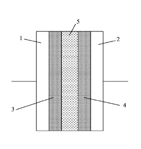
[0029] Figure 2 shows an embodiment of the disclosed energy storage device
that includes
electrodes 1 and 2 and the solid multilayer structure comprising two
insulating layers of an
insulating dielectric material (3 and 4) separated with one polarization layer
(5). In this embodiment
of the present invention, composite of polyaniline, PANI¨DBSA/PAA, synthesized
using in situ
polymerization of aniline in an aqueous dispersion of poly-acrylic acid (PAA)
in the presence of
dodecylbenzene sulfonate (DBSA) is used as the material of the polarization
layer, and polyethylene
is used as the insulating dielectric material. Thickness of the insulating
layer d1ns=2.5 nm. The
electrodes 10 and 11 are made of copper. Dielectric permittivity of
polyethylene is equal to 2.2 (i.e.
cills=2.2). The composite of polyaniline, PANI¨DBSA/PAA has the dielectric
permittivity Epoi equal
to 100,000 and thickness of the conductive layer possessing molecular
conductivity is d01 =1.0 mm.
Example 2
-20-
CA 02965870 2017-04-25
WO 2016/073522 PCT/US2015/058890
[0030] Figure 3 shows an embodiment of the disclosed energy storage device
that includes
electrodes 6 and 7 and the solid multilayer structure comprising alternating
insulating and
polarization layers, and wherein layers of an insulating dielectric material
(11, 12, 13, 14) are
separated by polarization layers (8, 9, 10). In this embodiment of the present
invention, PANI¨
DBSA/PAA composite is used as a material of the polarization layers and
polyethylene is used as an
insulating dielectric material. Thickness of the insulating layer d1n8=2.5 -
1000 urn. Electrodes 6 and
7 are made of copper. The dielectric permittivity of polyethylene is equal to
2.2 (i.e. gins=2.2) and
breakdown voltage Vbd = 40 kilovolt on thickness of 1 millimeter. In one
embodiment the a material
of the polarization layer is polyaniline (PANI) /poly(acrylic acid) (PAA)
composite which has the
dielectric permittivity Epoi equal to 100,000. In this example the thickness
of the polarization layer
d01 =1.0 ¨5.0 mm.
[0031] Although the present invention has been described in detail with
reference to a particular
preferred embodiment, persons possessing ordinary skill in the art to which
this invention pertains
will appreciate that various modifications and enhancements may be made
without departing from
the spirit and scope of the claims that follow.
[0032] While preferred embodiments of the present invention have been shown
and described
herein, it will be obvious to those skilled in the art that such embodiments
are provided by way of
example only. Numerous variations, changes, and substitutions will now occur
to those skilled in
the art without departing from the invention. It should be understood that
various alternatives to the
embodiments of the invention described herein may be employed in practicing
the invention. It is
intended that the following claims define the scope of the invention and that
methods and structures
within the scope of these claims and their equivalents be covered thereby.
-21-