Note: Descriptions are shown in the official language in which they were submitted.
CA 02966851 2017-05-04
WO 2016/075689
PCT/IL2015/051087
=
1
COMPACT HEAD-MOUNTED DISPLAY
SYSTEM PROTECTED BY A HYPERFINE STRUCTURE
Field of the Invention
The present invention relates to substrate-guided optical devices, and
particularly to devices which include a plurality of reflecting surfaces
carried by a
common light-transmissive substrate, also referred to as a light-guide
clement.
Background of the Invention
One important application for compact optical elements is in head-mounted
displays (HMDs), wherein an optical module serves both as an imaging lens and
a
conibiner, wherein a two-dimensional image source is imaged to infinity and
reflected
into the eye of an observer. The display source can be obtained directly from
either a
spatial light modulator (SLM) such as a cathode ray tube (CRT), a liquid
crystal display
(LCD), an organic light emitting diode array (OLED), a scanning source or
similar
devices, or indirectly, by means of a relay lens or an optical fiber bundle.
The display
source comprises an array of elements (pixels) imaged to infinity by a
collimating lens
and is transmitted into the eye of the viewer by means of a reflecting or
partially
reflecting surface acting as a combiner for non-see-through and see-through
applications, respectively. Typically, a conventional, free-space optical
module is used
for these purposes. As the desired field-of-view (FOV) of the system
increases,
however, such a conventional optical module becomes larger, heavier and
bulkier, and
therefore, even for a moderate performance device, such as a system, is
impractical.
This is a major drawback for all kinds of displays and especially in head-
mounted
applications, wherein the system should necessarily be as light and as compact
as
possible.
=
2
The strive for compactness has led to several different complex optical
solutions, all of which on the one hand, are still not sufficiently compact
for most
practical applications, and on the other hand, suffer major drawbacks in terms
of
manufacturability. Furthermore, the eye-motion-box (EMB) of the optical
viewing
angles resulting from these designs is usually very small, typically less than
8 mm.
Hence, the performance of the optical system is very sensitive, even for small
movements of the optical system relative to the eye of the viewer, and does
not allow
sufficient pupil motion for comfortable reading of text from such displays.
The teachings included in Publication Nos. WO 01/95027, WO 03/081320,
WO 2005/024485, WO 2005/024491, WO 2005/024969, WO 2005/124427,
WO 2006/013565, WO 2006/085309, WO 2006/085310, WO
2006/087709,
WO 2007/054928, WO 2007/093983, WO 2008/023367, WO
2008/129539,
WO 2008/149339, WO 2013/175465 and IL 232197, all in the name of Applicant,
are
noted for the reader's convenience .
Disclosure of the Invention
The present invention facilitates the exploitation of a very compact light-
guide
optical element (LOE) for, amongst other applications, HMDs. The invention
allows
relatively wide FOVs together with relatively large EMB values. The resulting
optical
system offers a large, high-quality image, which also accommodates large
movements
of the eye. The optical system offered by the present invention is
particularly
advantageous because it is substantially more compact than state-of-the-art
implementations, and yet it can be readily incorporated, even into optical
systems
having specialized configurations.
A broad object of the present invention is therefore to alleviate the
drawbacks of
prior art compact optical display devices and to provide other optical
components and
systems having improved performance, according to specific requirements.
The invention can be implemented to advantage in a large number of imaging
applications, such as portable DVDs, cellular phones, mobile TV receivers,
video
games, portable media players or any other mobile display devices.
The main physical principle of the LOE' s operation is that light waves are
trapped inside the substrate by total internal reflections from the external
surfaces of the
Date Recue/Date Received 2020-11-06
CA 02966851 2017-05-04
WO 2016/075689 PCT/1L2015/051087
3
LOE. However, there are situations wherein it is required to attach another
optical
element to at least one of the external surfaces. In that case, it is
essential to confirm that
on the one hand, the reflection of light waves from the external surfaces will
not be
degraded by this attachment, and on the other hand, that the coupling-out and
the
5 coupling-in
mechanisms of the light waves from and to the LOE will not be disturbed.
As a result, it is required to add at the external surfaces an angular
sensitive reflective
mechanism that will substantially reflect the entire light waves which are
coupled inside
the LOE and impinge on the surfaces at oblique angles, and substantially
transmit the
light waves which impinge on the surfaces close to a normal incidence.
10 In previous
inventions (e.g., described in Publication WO 2005/024491), a
reflective mechanism, wherein an angular sensitive thin film dielectric
coating is
applied to the surfaces of the LOE, has been illustrated. According to the
present
invention, an alternative reflective mechanism that utilizes an air gap film,
which
comprises a moth-eye structure, is presented. Moths' eyes have an unusual
property:
IS their surfaces are =
covered with a natural nanostructured film which eliminates
reflections. This allows the moth to see well in the dark, without
reflections, which give
its location away to predators. The structure consists of a hexagonal pattern
of bumps,
each roughly 200 nm high and their centers are spaced apart about 300 nm. This
kind of
anti-reflective coating works because the bumps are smaller than the
wavelength of
20 visible light, so
the light "sees" the surface as having a continuous refractive index
gradient between the air and the medium, which decreases reflection by
effectively
removing the air-lens interface. Practical anti-reflective films have been
made by
humans using this effect, being a form of bio-mimicry. Moth eye replicas show
that
reflectance for normally incident light is virtually completely eliminated for
these
= 25 structures. Optical modeling and experiments with other shapes
and dimensions of such
dense uneven hyperfine periodic structures prove that it is possible to
suppress
reflection in wider wavelength range (from UV to IR) and wider light incidence
angles
(0 60 degrees).
According to the present invention the moth-eye film, or any similar hyperfine
30 structure, is not
utilized as anti-reflection film. Instead, the special hyperfine structure is
exploited as the required angular sensitive reflective mechanism. When it is
required to
attach an optical element to the external surface of the LOE, an air gap film
is cemented
CA 02966851 2017-05-04
WO 2016/075689 PCT/1L2015/051087
4
to the optical element such that the hyperfine structure faces the LOE after
the
attachment. Therefore, when the coupled-in light waves inside the LOE impinge
on the
hyperfine structure at different oblique angles, they "see" only the external
part of the
periodic structure. The actual refractive index, which is "seen" by the
incoming optical
light waves is, therefore, close to the refractive index of the air, and the
total internal
reflection mechanism is preserved. On the other hand, the air gap film is
substantially
transparent to the incoming light waves from the external scene or to the
light waves
which are coupled out from the LOE.
The invention therefore provides an optical system, including a light-
transmitting
substrate having at least two external major surfaces and edges, an optical
element for
coupling light waves into the substrate by internal reflection, at least one
partially
reflecting surface located in the substrate, for coupling light waves out of
the substrate,
at least one transparent air gap film including a base and a hyperfine
structure defining a
relief formation, constructed on the base, wherein the air gap film is
attached to one of
the major surfaces of the substrate, with the relief formation facing the
substrate
defining an interfae,e plane, so that the light waves coupled inside the
substrate are
substantially totally reflected from the interface plane.
Brief Description of the Drawings
The invention is described in connection with certain preferred embodiments,
with reference to the following illustrative figures so that it may be more
fully
understood.
With specific reference to the figures in detail, it is stressed that the
particulars
shown arc by way of example and for purposes of illustrative discussion of the
preferred
embodiments of the present invention only, and are presented in the cause of
providing
what is believed to be the most useful and readily understood description of
the
principles and conceptual aspects of the invention. In this regard, no attempt
is made to
show structural details of the invention in more detail than is necessary for
a
fundamental understanding of the invention. The description taken with the
drawings
are to serve as direction to those skilled in the art as to how the several
forms of the
invention may be embodied in practice.
CA 02966851 2017-05-04
WO 2016/075689 PCT/1L2015/051087
In the drawings:
Fig. 1 is a side view of an exemplary, prior art LOE;
Fig. 2 is a schematic diagram illustrating a prior art optical device for
collimating input light-waves from a display light source;
5 Fig. 3 is a schematic diagram illustrating a prior art system for
collimating and
coupling-in input light-waves from a display light source into an LOE;
Fig. 4 is a schematic diagram illustrating another prior art system for
collimating
and coupling-in input light-waves from a display light source into a
substrate, wherein
the collimating module is attached to the substrate;
10 Fig. 5 illustrates an exemplary embodiment of the present invention,
wherein a
negative lens is attached to an external surface of the light-guide optical
element, in
= accordance with the present invention;
Fig. 6 illustrates an exemplary embodiment of the present invention, wherein
negative and positive lenses are attached to the external surfaces of the
light-guide
15 optical element, in accordance with the present invention;
Figs. 7a and 7b are two- and three-dimensional schematic views of an exemplary
embodiment of an air gap film, wherein a hyper-fine periodic structure of
transparent
dielectric material arranged at a small pitch shorter than the wavelengths of
the photopic
= region, is constructed on a flat transparent substrate;
20 Figs. 8a and 8b respectively illustrate a side view and a top view of
an
exemplary air gap film;
Figs. 9a and 9b respectively illustrate a side view and a top view of an
exemplary air gap film for an internal cross section which is close to the
base;
Figs. 10a and 10b respectively illustrate a side view and a top view of an
25 exemplary air gap film for an external cross section which is close to
the air;
Fig. 11 illustrates a side view of a light wave impinging on the upper side of
a
hyperfine structure at an oblique angle, in accordance with the present
invention;
Fig. 12 illustrates an air-gap film which is attached to the external surface
of an
LOE, wherein a coupled light wave impinges on the interface surface between
the LOE
30 and the film, in accordance with the present invention;
Figs. I 3a and 13b respectively illustrate a front view of an eyeglasses
system
and a top view of an LOE embedded between two optical lenses and assembled
inside
the eyeglasses frame, in accordance with the present invention;
CA 02966851 2017-05-04
WO 2016/075689 PCT/1L2015/051087
6
Figs. 14a, 14b and 14c respectively illustrate a non-monolithic optical
element
comprising an LOE embedded between a front positive lens and a rear negative
lens,
mounted together inside a frame without adhesive, in accordance with the
present
invention;
Figs. 15a, 15b and 15c respectively illustrate an alternative method for
embedding an LOE between two optical lenses, utilizing a peripheral bonding
technique, in accordance with the present invention;
Figs. 16a, 16b and 16c respectively illustrate an alternative method for
monolithically embedding an LOE between two optical lenses, in accordance with
the
present invention, and
Figs. 17a, 17b and 17c respectively illustrate an LOE embedded between two
flat substrates and assembled inside a frame, in accordance with the present
invention.
Fig. 18 illustrates an exemplary embodiment of the present invention, wherein
the coupling-in as well as the coupling-out elements are diffractive optical
elements,
and
Fig. 19 illustrates an exemplary embodiment of the present invention, wherein
the optical module is embedded in a hand-carried display system.
Detailed Description of Embodiments
Fig. 1 illustrates a sectional view of a prior art optical system including a
planar
substrate 20 and associated components (hereinafter also referred to as an
utilizable in the present invention. An optical means, e.g., a reflecting
surface 16, is
illuminated by light waves 18, which arc collimated from a display of a light
source (not
shown). The reflecting surface 16 reflects incident light waves from the
source, such
that the light waves are trapped inside the planar substrate 20 of the LOE, by
total
internal reflection. After several reflections of the major lower and upper
surfaces 26,
28 of the substrate 20, the trapped waves reach an array of selective
partially reflecting
surfaces 22, which couple the light out of the substrate into a pupil 25 of an
eye 24 of a
viewer. Herein, the input surface of the LOE will be regarded as the surface
through
which the input light waves enter the LOE, and the output surface of the LOE
will be
regarded as the surface through which the trapped waves exit the LOE. In the
case of
the LOE illustrated in Fig. 1, both the input and the output surfaces are on
the lower
CA 02966851 2017-05-04
WO 2016/075689
PCT/IL2015/051087
7
surface 26. Other configurations, however, are envisioned in which the input
and the
image waves could be located on opposite sides of the substrate 20, or when
the light is
coupled into the LOE through a slanted edge of the substrate.
As illustrated in Fig. 2, the s-polarized input light-waves 2 from a display
light
5 source 4 are coupled into a collimating module 6 through its lower
surface 30, which
module is usually composed of a light-waves transmitting material. Following
reflection-off of a polarizing beamsplitter 31, the light-waves are coupled-
out of the
substrate through surface 32 of the collimating module 6. The light-waves then
pass
through a quarter-wavelength retardation plate 34, reflected by a reflecting
optical
10 element 36, e.g., a flat mirror, return to pass again through the
retardation plate 34, and
re-enter the collimating module 6 through surface 32. The now p-polarized
light-waves
pass through the polarizing beamsplitter 31 and are coupled out of the light-
guide
through surface 38 of the collimating module 6. The light-waves then pass
through a
second quarter-wavelength retardation plate 40, collimated by a component 42,
e.g., a
15 lens, at its reflecting surface 44, return to pass again through the
retardation plate 34,
and re-enter the collimating module 6 through surface 38. The now s-polarized
light-
waves reflect off the polarizing beamsplitter 31 and exit the collimating
module through
the upper surface 46. The reflecting surfaces 36 and 44 can be materialized
either by a
metallic or a dielectric coating.
20 Fig. 3 illustrates how a collimating module 6, constituted by the
components
detailed with respect to Fig. 2, can be combined with a substrate 20, to form
an optical
system. The output light-waves 48 from the collimating module 6 enter the
substrate 20
through its lower surface 26. The light waves entering the substrate 20 are
reflected
from optical element 16 and trapped in the substrate, as illustrated in Fig.
2. Now, the
25 collimating module 6, comprising the display light source 4, the folding
prisms 52 and
54, the polarizing beamsplitter 31, the retardation plates 34 and 40 and the
reflecting
= optical elements 36 and 42, can easily be integrated into a single
mechanical module
and assembled independently of the substrate, even with non-accurate
mechanical
tolerances. In addition, the retardation plates 34 and 40 and the reflecting
optical
30 elements 36 and 42 could be cemented together, respectively, to form
single elements.
It would be advantageous to attach all the various components of the
collimating
module 6 to the substrate 26, to form a single compact element resulting in a
simplified
CA 02966851 2017-05-04
WO 2016/075689
PCT/IL2015/051087
8
mechanical module. Fig. 4 illustrates such a module, wherein the upper surface
46 of
the collimating module 6 is attached at thc interface plane 58, to the lower
surface 26 of
the substrate 20. The main problem of this configuration is that the attaching
procedure
cancels the previously existing air gap 50 (illustrated in Fig. 3) between the
substrate 20
5 and the collimating
module 6. This air gap is essential for trapping the input light waves
48 inside the substrate 20. The trapped light waves 48 should be reflected at
points 62
and 64 of the interface plane 58. Therefore, a reflecting mechanism should be
applied at
this plane, either at the major surface 26 of the substrate 20, or at the
upper surface 46 of
the collimating module 6. A simple reflecting coating cannot, however, be
easily
10 applied, since
these surfaces should also be transparent to the light waves that enter and
exit the substrate 20 at the exemplary points 66. The light waves should pass
through
plane 48 at small incident angles, and reflect at higher incident angles.
Usually, the
passing incident angles are between 0 and 150 and the reflecting incident
angles are
between 40 and 80 .
15 In the above-
described embodiments of the present invention, the image which
is coupled into the LOE is collimated to infinity. There are applications,
however,
= where the transmitted image should be focused to a closer distance, for
example, for
people who suffer from myopia and cannot properly see images located at long
distances. Fig. 5 illustrates an optical system utilizing a lens, according to
the present
20 invention. An image
80 from infinity is coupled into a substrate 20 by a reflecting
surface 16, and then reflected by an array of partially reflective surfaces 22
into the eye
24 of the viewer. The (plano-concave) lens 82 focuses the images to a
convenient
distance and optionally corrects other aberrations of the viewer's eye,
including
astigmatism. The lens 82 can be attached to the surface of the substrate at
its flat surface
25 84. As explained
above with regard to Fig. 4, a thin air gap must be preserved between
the lens and the substrate, to ensure the trapping of the image light waves 80
inside the
substrate by total internal reflection.
In addition, in most of the applications related to the present invention, it
is
assumed that the external scene is located at infinity; however, there are
professional or
30 medical
applications where the external scene is located at closer distances. Fig. 6
= illustrates an optical system for implementing a dual lens configuration,
based on the
present invention. Image light waves 80 from infinity are coupled into a
substrate 20 by
=
CA 02966851 2017-05-04
WO 2016/075689 PCT/IL2015/051087
9
a reflecting surface 16 and then reflected by an array of partially reflective
surfaces 22
into the cyc 24 of the viewer. Another image 86 from a close distance scene is
collimated to infinity by a lens 88 and then passed through the substrate 20
into the eye
24 of a viewer. The lens 82 focuses images 80 and 86 to a convenient distance,
usually
(but not necessarily always) the original distance of the external scene
image, and
corrects other aberrations of the viewer's eye, if required.
The lenses 82 and 88 shown in Figs. 5 and 6 are simple piano-concave and
piano-convex lenses, respectively, however, to keep the planar shape of the
substrate, it
is possible instead to utilize Fresnel lenses, which can be made of thin
molded plastic
plates with fine steps. Moreover, an alternative way to materialize the lenses
82 or 88,
instead of utilizing fixed lenses as described above, is to use electronically
controlled
dynamic lenses. There are applications whem the user will not only be able to
sec a non-
collimated image but also to dynamically control the focus of the image. It
has been
shown that a high resolution, spatial light modulator (SLM) can be used to
form a
holographic clement. Presently, the most popular sources for that purpose are
LCD
devices, but other dynamic SLM devices can be used as well. High resolution,
dynamic
lenses having several hundred lines/mm are known. This kind of electro-
optically
controlled lenses can be used as the desired dynamic elements in the present
invention,
instead of the fixed lenses described above in conjunction with Figs. 5 and 6.
Therefore,
in real time, a user can determine and set the exact focal planes of both the
virtual image
projected by the substrate and the real image of the external view.
As illustrated in Fig. 6, it would be advantageous to attach the lenses 82 and
88
to the substrate 20, to form a single, compact simplified mechanical module.
Clearly,
the main problem as hereinbefore described, is that the attaching procedure
cancels the
previously existing air gap between the substrate 20 and the lenses 82 and 88,
which
gaps are essential for trapping image light waves 80 inside the substrate 20.
The trapped
image light waves 80 should be reflected at point 90 of the interface plane 84
and
transmitted through the same plane at point 92. Therefore, a similar partially
reflecting
mechanism as described above in relation to Fig. 4 should be applied at this
plane.
To achieve the required partially reflecting mechanism, it is possible to
apply an
angular sensitive thin film coating at the major surfaces of the substrate;
however, the
fabrication of this embodiment can be complicated and expensive. An
alternative way
CA 02966851 2017-05-04
WO 2016/075689 PCT/1L2015/051087
for realizing the required partially reflecting mechanism is to attach a
transparent air gap
film 110 to thc major surfaces of the substrate, as illustrated in Figs. 7a
and 7b. The
term air gap film relates to an optical device which has on its surface a
hyper-line
periodic structure 111 of transparent dielectric material arranged at a small
pitch shorter
5 than the wavelengths of the photopic region, e.g., an optical device such
as moth-eye
film having a dense (uneven) hyperfine periodic structure 111 (hereinafter
referred to as
"relief formation"), which is constructed on a flat transparent substrate 112
(hereinafter
referred to as "base" 112 or "base film" 112). The height of the relief
formation should
preferably (but not necessarily always) be less than 1 micron.
10 As seen in Figs. 8a, and 8b, any cross section 121 parallel to the
surface of the
= air gap film 110 has a periodic formation, wherein the proportional
portion of the
dielectric material 123 in the relief formation is changed gradually as a
function from
the film itself.
As further seen in Figs. 9a, 9b and 10a and 10b, in the internal cross section
124,
15 which is close to the base film 112, i.e., the lower portion of the
hyperfine structure 111,
the proportional portion of the dielectric material 125 in the relief
formation 126 is
maximal and substantially close to 1, while in the external cross section 127,
i.e., close
to the upper portion of the hyperfine structure 111, the proportional portion
of the
dielectric material 128 in the relief formation 129 is minimal, namely,
significantly
20 lower than in material 125, and substantially equal to zero.
Typically, when light waves pass through an optical device having a periodic
structure, diffraction of light occurs and the brightness of the zero order of
the diffracted
light, namely, the light which is transmitted through the device without any
diffraction,
is considerably reduced. When the pitch of the hyper-fine periodic structure
is, however,
25 considerably shorter than the wavelength of the incoming light waves, no
diffraction
occurs. Instead, since the optical waves "see" a medium having a refractive
index which
is the average of the materials contained in this medium, effective anti-
reflection
properties can be obtained.
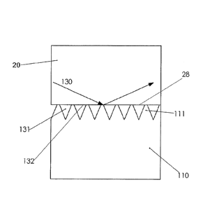
On the other hand, as illustrated in Fig. 11, when the light waves 130 impinge
on
30 the periodic hyperfine structure 1 1 1 at the upper side of the
structure at oblique angles,
they "sec" only the external part of the periodic structure, wherein the
proportional part
CA 02966851 2017-05-04
WO 2016/075689 PCT/1L2015/051087
11
of the transparent material is very low. Therefore, the actual refractive
index, which is
"seen" by the incoming optical waves, is close to the refractive index of the
air 131.
As a result, and as illustrated in Fig. 12, when such an air-gap film is
attached to
the external surface 28 of the substrate 20, the coupled light waves 130
impinge on the
interface surface 132 between the substrate and the film at angles higher than
the critical
angle, the air 131 confined between the film and the substrate provides an
optical
isolation due to the air-like refractive index in the boundary surface.
Therefore, the
phenomena of total internal reflection of the coupled-in light waves from the
external
surface will be preserved and the light waves will be contained inside the
substrate.
The geometrical characteristic of the hyperfine structure, such as the height,
peak-to-peak and width thereof, can usually be between 10 to 800 nanometers.
In
addition, the exact shape and of the hyperfine structure should not
necessarily be that of
the moth eye. Any other nano-structure shape, such as pyramids, prisms, cones
and
others, can be utilized. Moreover, the hyperfine structure should not
necessarily be
specifically periodic, although a periodic structure is usually easier to
fabricate. This
hyperfine structure, however, should fulfill the following requirements: on
one hand,
the structure should be solid enough not to collapse during the attaching
process and, on
the other hand, the proportional portion of the dielectric material in the
external cross-
section of the structure, should be substantially equal to zero, to maintain
the total
internal reflection phenomena inside the substrate. In addition, the size of
the basic
elements of the hyperfine structure should not be too large, in order to avoid
diffraction
effects. Reducing the thickness of the hyperfine structure to below 100 nm,
however,
might undesirably allow the penetration of the trapped waves through the air
gap film
and the deterioration of the total internal reflection phenomena. As a result,
a typical
required value for the hyperfine structure thickness is between 200 and 300
nm.
Fig. 13a illustrates a front view of an eyeglasses system 140 and Fig. 13b a
top
view of a substrate 20 which is embedded between two optical lenses 141, 142
and
assembled inside the eyeglasses frame 143. As seen, in addition to the optical
elements,
the frame can contain other accessories including a camera 144, a microphone
145,
earphones 146, USB connectors, memory cards, an inertial measurement unit
(IMU),
and the like.
=
CA 02966851 2017-05-04
WO 2016/075689 PCT/1L2015/051087
12
Figs. 14a, 14b and 14c illustrate a non-monolithic optical element 150
comprising a substrate 20 embedded between front positive lens 151 and rear
negative
lens 152, mounted together inside a frame 154 without adhesive. Air gap films
110 (Fig.
14c) are placed or bonded between the substrate 20 and the lenses 151, 152,
wherein the
hyperfine structures 111, respectively face the external surfaces 26 and 28 of
the
substrate 20. The air gap films 110 can be directly cemented on the planar
surfaces of
the optical lenses 151 and 152 using pressure-sensitive adhesive (PSA), or can
be
fabricated directly as an integral part of the lenses utilizing embossing,
injection
molding, casting, machining, soft lithography or any other direct fabrication
method.
The embedded optical element 150 can be assembled inside the frame 154
utilizing
pressure or cementing techniques.
An alternative method for monolithically embedding the substrate 20 between
the two optical lenses is illustrated in Figs. 15a, 15b and 15c. The substrate
20 is
embedded between the optical lenses utilizing a peripheral bonding technique.
The front
lens 151 and rear lens 152 are cemented to the peripheral edges of the
substrate 20 using
non-optical adhesive or any other high-viscosity adhesive 156 that mount all
components together. The viscosity of the adhesive should be high enough in
order to
prevent leakage of the adhesive into the air pockets 131, which are confined
between
the film 110 and the substrate 20. Such a leakage can eliminate the air gap
which is
required to preserve the total internal reflection of the light waves from the
external
surfaces of the substrate. The required adhesive 156 can, for example, be OP-
67-LS or
any room temperature vulcanization (RTV)
Another alternative method for monolithically embedding the substrate 20
between the two oPtical lenses is illustrated in Figs. 16a, 16b and 16e. The
production
.. procedure of the embedded element is as follows: Placing the air gap film
110, with the
hyperfine structures 111 facing the external surfaces 26 and 28 of the
substrate 20;
utilizing attaching techniques such as static electricity; preparing a mold
160 having the
required external shape of the element; inserting the substrate 20 into the
mold; casting
or injecting the polymer into the mold, curing the polymer by UV or by
changing the
polymer temperature, and finally, ejecting the embedded element from the mold.
As
explained above in relation to Figs. 15a to 15c, it is also important that the
hyperfine
regions will be isolated from the injected material during the injection
molding process,
CA 02966851 2017-05-04
WO 2016/075689 PCT/IL2015/051087
13
in order to prevent a leakage of the material into the air pockets 131 between
the
substrate 20 and the air gap film 110.
Figs. 13a to 16c illustrate different methods for forming an optical component
comprising a substrate embedded between two optical lenses, however, there arc
embodiments wherein it is required to attach planar elements to the external
surfaces of
the substrate. An example for such an embodiment is illustrated in Fig. 4,
wherein the
collimating element 6 is attached to the substrate 20. Other reasons for
attaching a flat
element to a substrate can be for mechanically protecting the substrate to
enhance the
user's eye-safety, or applying a coating on the external surface of the flat
element to
to achieve various characteristics such as, photochromic response, scratch
resistance,
super-hydrophobicity, tinted (colored) view, polarization, anti-finger print,
and the like.
A substrate 20 embedded between two flat substrates 162 and 164 and
assembled inside frames 166, 167 is illustrated in Figs. 17a, 17b and 17c. The
embedding process of the substrate and the flat substrates 20 can be
materialized
utilizing mechanical attachment, peripheral cementing or monolithic
fabrication.
Embedding processes can include attaching only a single element to one of the
external
surfaces of the substrate or combining different elements, such as flat
substrates as well
as curved lenses.
In all the embodiments illustrated so far the element for coupling light waves
out
of the substrate is at least one flat partially reflecting surface located in
said substrate,
which is usually coated with a partially reflecting dielectric coating and is
non-parallel
to the major surfaces of said substrate. However, the special reflective
mechanism
according to the present invention can be exploited also for other coupling-
out
technologies. Fig. 18 illustrates a substrate 20, wherein the coupling-in
element 170 or
the coupling-out element 172 are diffractive elements. In addition, other
coupling-out
elements, such as a curved partially reflecting surface, and other means, can
be used.
The embodiments of Figs. 13-17 are just examples illustrating the simple
implementation of the present invention. Since the substrate-guided optical
element,
constituting the core of the system, is very compact and lightweight, it could
be
installed in a vast variety of arrangements. Many other embodiments are also
possible,
including a visor, a folding display, a monocle, and many more. This
embodiment is
designated for applications where the display should be near-to-eye; head-
mounted,
CA 02966851 2017-05-04
WO 2016/075689 PCT/IL2015/051087
14
head-worn or head-carried. There are, however, applications where the display
is
located differently. An example of such an application is a hand-carried
device for
mobile application, such as, for example, a smartphone or smartwatch. The main
problem of these smart devices is the contradiction between the required small
size and
volume and the desired high quality image.
Fig. 19 illustrates an alternative method, based on the present invention,
which
eliminates the current necessary compromise between the small size of mobile
devices
and the desire to view digital content on a full format display. This
application is a
hand-held display (HHD) which resolves the previously opposing requirements,
of
achieving small mobile devices, and the desire to view digital content on a
full format
display, by projecting high quality images directly into the eye of the user.
An optical
module including the display source 4, the folding and collimating optics 190
and the
substrate 20 is integrated into the body of a smart device 210, where the
substrate 20
replaces the existing protective cover-window of the phone. Specifically, the
volume of
.. the support components, including source 4 and optics 190, is sufficiently
small to fit
inside the acceptable volume for modern smart device. In order to view the
full screen,
transmitted by the device, the window of the device is positioned in front of
the user's
eye 24, observing the image with high FOV, a large eye-motion-box and a
comfortable
eye-relief. It is also possible to view the entire FOV at a larger eye-relief
by tilting the
device to display different portions of the image. Furthermore, since the
optical module
can operate in see-through configuration, a dual operation of the device is
possible;
namely there is an option to maintain the conventional display 212 intact. In
this
manner, the standard display can be viewed through the substrate 20 when the
display
source 4 is shut-off. In a second, virtual-mode, designated for massive
internet surfing,
or high quality video operations, the conventional display 212 is shut-off,
while the
display source 4 projects the required wide FOV image into the eye of the
viewer
through the substrate 20. Usually, in most of the hand-carried smart devices,
the user
can operate the smart device by using a touchscreen which is embedded on the
front
window of the device. As illustrated in Fig. 19, the touchscreen 220 can be
attached to a
smart device by directly cementing it on the external surface air gap films
110, which is
located on the substrate 20.