Note: Descriptions are shown in the official language in which they were submitted.
CA 02967555 2017-05-11
CHIP FUSE MANUFACTURING METHOD AND CHIP FUSE
TECHNICAL FIELD
[0001] The present invention relates to a method for manufacturing a chip fuse
and to
a chip fuse.
BACKGROUND OF THE INVENTION
[0002] Fuses are used in order to prevent occurrence of circuit breakdown due
to an
inflow of excess current caused by a failure, or the like, in an electronic
device.
Recently, with the miniaturization of devices, chip fuses have been employed
that are
easily surface-mounted on wiring boards, etc., and that excel in high-volume
production.
In a chip fuse, a fuse element made of a metal foil is formed on an insulating
substrate,
such as a ceramic substrate, etc., (hereinafter, also simply referred to as a
substrate).
[0003] It has been requested, in chip fuses, to reduce a melting current that
melts the
fuse element (to, for example, 100mA or less); namely, to reduce the capacity.
Various
proposals have been made in order to respond to such request.
[0004] For example, Patent Document 1 described below discloses a fuse in
which a
tin core is surrounded by a silver casing. In addition, Patent Document 2
described
below discloses a fuse in which tin is coated over a copper fuse link. With
the
technology of Patent Document 1 and Patent Document 2, when the fuse element
melts,
tin with a low melting point melts first, becomes diffused in silver or
copper, and lowers
a melting point of the fuse element, and thus, the melting current of the fuse
may be
reduced.
[0005] Moreover, Patent Document 3 discloses the technology by which a fuse
part is
formed on a silicone substrate and a hollow part is formed directly under the
fuse part of
1
CA 02967555 2017-05-11
the substrate by means of etching. Since heat loss to the substrate can be
reduced by
forming the hollow part, a reduction in the melting current of the fuse may be
expected.
PRIOR ART
PATENT DOCUMENT
=
[0006] Patent Document 1: Japanese Unexamined Patent Application Publication
No.
2005-505110
Patent Document 2: Japanese Unexamined Patent Application Publication No.
2009-509308
Patent Document 3: Japanese Unexamined Patent Application Publication No.
2007-095592
SUMMARY OF INVENTION
PROBLEMS TO BE SOLVED BY THE INVENTION
[0007] However, with the technology of Patent Document 1 and Patent Document
2,
the manufacturing cost increases due to the multilayered structures. Moreover,
there is
a risk that tin may be diffused unnecessarily in silver or copper.
Furthermore, with the
technology of Patent Document 3, there is a risk that the chip fuse cost
increases since
significant man-hours are needed for the process of etching the substrate.
[0008] In addition, a rush current (also referred to as an inrush current) is
known to
occur at the time of switching on and/or off the power supply to the circuit.
Accordingly, as to the chip fuse, it is required that it melts when an
abnormal current
flows therethrough but that it tolerates and does not melt when the rush
current occurs at
the time of switching on and/or off the power supply (in other words, it is
required that
it has a high rush resistance).
2
CA 02967555 2017-05-11
[0009] Accordingly, the present invention has been made in view of these
points and
an object thereof is to provide a reduced capacity and high rush resistant
chip fuse at a
low price.
MEANS FOR SOLVING THE PROBLEMS
[0010] In a first aspect of the present invention, a method for manufacturing
a chip
fuse is provided, which comprises: a liquid film forming step for forming a
liquid film
= of dispersion liquid having metal nanoparticles dispersed therein on a
principal surface
of a substrate; a fuse film forming step for forming a fuse film on the
principal surface
by irradiating the liquid film with laser light; a first terminal forming step
for forming
first terminals that each connects to the fuse film on each of both end sides
in a
longitudinal direction of the fuse film on the principal surface; a covering
part forming
= step for forming a covering part that covers a central portion in the
longitudinal
direction of the fuse film; and a second terminal forming step for forming
second
terminals that electrically connect to the first terminals.
[0011] The first terminal forming step may irradiate part of the liquid film
corresponding to the first terminals with the laser light to form the first
terminals.
= [0012] The first terminal forming step may form a first terminal group
including a
plurality of first terminals that are separated from each other in the
longitudinal
direction on each of both end sides in the longitudinal direction of the fuse
film on the
principal surface.
[0013] The covering part forming step may form the covering part to cover a
central-portion first terminal that is located closest to the central portion
among the first
terminal group in the longitudinal direction, and the second terminal forming
step forms
the second terminal that connects to an end-side first terminal among the
first terminal
3
CA 02967555 2017-05-11
group, the end-side first terminal being located on an end side in the
longitudinal
direction.
[0014] The fuse film forming step may form the fuse film in a linear form or a
curved
form having a width corresponding to a spot diameter of the laser light by
scanning the
liquid film once with the laser light.
[0015] The liquid film forming step may form, based on the correspondence
between a
first thickness of the liquid film prior to the irradiation of the laser light
and a second
thickness that is smaller than the first thickness of the fuse film after the
irradiation of
the laser light, the liquid film by adjusting the first thickness.
[0016] The fuse film forming step may irradiate the liquid film with the laser
light by
adjusting at least one of irradiation velocity or irradiation intensity of the
laser light
from a laser irradiation apparatus, depending on a thickness of the liquid
film.
[0017] In the above-described method for manufacturing a chip fuse, the
substrate is
= an aggregated substrate on which a plurality of the fuse films are
formed, and the
method further comprises: a mark forming step for forming a positional
adjustment
mark for adjusting formation positions of the plurality of fuse films on the
aggregated
substrate by irradiating the liquid film with the laser light, and the fuse
film forming
step may form each of the plurality of fuse films based on the position of the
formed
= positional adjustment mark.
[0018] The fuse film forming step may attenuate the laser light oscillated by
an
oscillation part of the laser irradiation apparatus with an attenuation
optical filter and
may irradiate the liquid film with the attenuated laser light.
[0019] In a second aspect of the present invention, a chip fuse is provided,
which
comprises: a substrate; a fuse film provided on a principal surface of the
substrate; a
= 4
CA 02967555 2017-05-11
first terminal group including a plurality of first terminals that are
separated from each
other in a longitudinal direction of the fuse film on the principal surface,
the first
terminal group being provided on each of both end sides of the longitudinal
direction to
connect to the fuse film; a covering part that covers a central portion in the
longitudinal
direction of the fuse film; and a second terminal that electrically connects
to one or
more of the plurality of first terminals of the first terminal group, on both
end sides in
the longitudinal direction.
[0020] In the above-described chip fuse, each first terminal of the first
terminal group
may be provided along an intersecting direction that intersects with the
longitudinal
direction of the fuse film, and the width of each first terminal of the first
terminal group
may be the same as the width of the fuse film.
[0021] In the above-described chip fuse, the thickness of each first terminal
of the first
terminal group may be the same as the thickness of the fuse film.
[0022] In the above-described chip fuse, the covering part may also cover the
first
terminal that is located closest to the central portion in the longitudinal
direction among
the first terminal group.
[0023] In the above-described chip fuse, a melting current density, which is
obtained
by dividing a melting current that melts the fuse film by a cross-sectional
area that is
orthogonal to the longitudinal direction of the fuse film, may be 4.0 x 10⁶
(A/cm2) or
less.
[0024] In the above-described chip fuse, a specific surface area, which is
obtained by
dividing a surface area of the fuse film by a volume of the fuse film, may be
21 (/ttm) or
less.
= 5
CA 02967555 2017-05-11
[0025] In the above-described chip fuse, when assuming the width of the fuse
film to
be width w and the thickness of the fuse film to be film thickness t, the
width w may be
between 3 (p.m) and 20 (pm), inclusive; and the film thickness t may be
between 0.1
(p.m) and 3.0 (p.m), inclusive.
[0026] In the above-described chip fuse, thermal conductivities of both the
substrate
and the covering part may be 0.3 (W/m = K) or less.
[0027] In the above-described chip fuse, the length of the fuse film between
the first
terminals, each of which is located on the central portion, among the first
terminal
groups on both end sides in the longitudinal direction, may be 600 ( m) or
more.
EFFECT OF THE INVENTION
[0028] According to the present invention, an effect whereby a reduced
capacity and a
high rush resistant chip fuse can be provided at a low cost is achieved.
BRIEF DESCRIPTION OF THE DRAWINGS
[0029] FIG. 1 is a schematic cross-sectional diagram of a chip fuse 1
according to an
embodiment of the present invention.
FIG. 2 is a schematic plan view of a chip fuse 1.
FIG. 3 is a graph showing a pre-arcing time-current characteristic curve of a
chip fuse 1.
FIG. 4 is a schematic cross-sectional diagram of a chip fuse 900, which is a
target of the analysis.
FIG. 5 is a schematic plan view of a chip fuse 900, which is a target of the
analysis.
FIG. 6 is a cross-sectional diagram through I-I in FIG. 5.
FIG. 7 is a graph showing experimental results.
6
=
CA 02967555 2017-05-11
FIG. 8 is a graph showing the relationship between the fuse element length and
the minimum melting current density, which is derived from the experimental
results of
FIG. 7.
FIG. 9 is a graph showing experimental results.
FIG. 10 is a graph showing experimental results.
FIG. 11 is a graph showing an example of the relationship between the
thickness t of the fuse element 920 and the specific surface areas 41, E,2, 43
thereof.
FIG. 12 is a graph showing the relationship between: the thickness t of the
fuse
element 920; and the minimum melting current 'min and the conducting cross-
sectional
area Ao thereof.
FIG. 13 is a graph showing the relationship between: the thickness t of the
fuse
element 920; and the minimum melting current density (1/A4-flo and the
specific surface
area 4ithereof.
FIG. 14 is a graph showing the relationship between the specific surface area
41
and the minimum melting current density (1/A0)mm=
FIG. 15 is a table summarizing the correlations among the width w, the
thickness t and the specific surface areas 41 to 43 of the fuse element 920.
FIG. 16 is a table summarizing the relationship between the t/w ratio and the
minimum melting current density (1/A)min.
FIG. 17 is a diagram for explaining the relationship between the rush current
and the pre-arcing time-current characteristic curve.
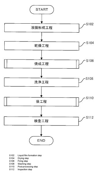
FIG. 18 is a flowchart showing the manufacturing process of the chip fuse 1.
FIG. 19 is a schematic diagram showing an ink film 110 formed on an
aggregated substrate 100.
= 7
CA 02967555 2017-05-11
FIG. 20 is a schematic diagram showing an example of the configuration of a
laser irradiation apparatus 200.
FIG. 21 is a flowchart showing the details of the firing process.
FIG. 22 is a diagram showing the aggregated substrate 100 after the firing.
FIG. 23 is a diagram showing the condition in which the internal terminal
groups 130 are formed with respect to the fuse film 120.
FIG. 24 is a flowchart showing the details of the post-process.
FIG. 25 is a diagram showing the condition in which an overcoat 140 is formed
on a sub-assembly 118.
FIG. 26 is a diagram showing the condition after external terminals 151, 152
are formed.
FIG. 27 is a diagram for explaining the stamping of a seal onto the overcoat
140.
FIG. 28 is a graph showing the relationship between the thickness t(i) of the
ink
film prior to the firing and the thickness t of the fuse film after the
firing.
FIG. 29 is a graph showing the relationship between the spot diameter (19 of
the
laser light and the width w of the fuse film 120.
DETAILED DESCRIPTION OF THE INVENTION
[0030] In the following, the description will be given in the order indicated
below.
1. Configuration of chip fuse
2. Theoretical analysis of chip fuse pre-arcing time-current characteristics
3. Studies leading up to the invention of the present application
3-1. First study
3-2. Second study
8
CA 02967555 2017-05-11
3-3. Third study
3-4. Fourth study
4. Method for manufacturing chip fuse
5. Study regarding the firing of ink film
6. Variation
[0031]
<1. Configuration of chip fuse>
The configuration of a chip fuse 1 according to an embodiment of the present
invention
will now be described with reference to FIGs. 1 and 2. FIG. 1 is a schematic
cross-sectional diagram of a chip fuse 1 according to an embodiment. FIG. 2 is
a
schematic plan view of the chip fuse 1.
[0032] The chip fuse 1 is surface-mounted on a circuit substrate, etc. of an
electronic
device and melts when an abnormal current flows in the circuit. As shown in
FIGs. 1
and 2, the chip fuse 1 includes a support substrate 10, a fuse film 20,
internal terminal
groups 31, 32, an overcoat 40 and external terminals 51, 52.
[0033] The support substrate 10 is a substrate for supporting the fuse film 20
and the
internal terminal groups 31, 32. The support substrate 10 is, for example, a
polyimide
substrate. The thickness of the support substrate 10 is approximately 250
(p.m) and the
surface roughness Ra thereof is approximately 0.05 ( m). Additionally, the
thermal
conductivity of the support substrate 10 is 0.3 (W/m = K) or less.
[0034] The fuse film 20 is provided on the principal surface 12 of the support
substrate
10. Although the
details thereof are described hereinafter, the fuse film 20 is formed
on the principal surface 12 by firing an ink film containing metal
nanoparticles. As the
metal nanoparticles, for example, silver nanoparticles are used.
9
CA 02967555 2017-05-11
[0035] In the present embodiment, the melting current density, which is
obtained by
dividing the melting current that melts the fuse film 20 by the cross-
sectional area that is
orthogonal to the longitudinal direction of the fuse film 20, is 4.0 x 10⁶
(A/cm2) or less.
Desirably, it is preferable for the melting current density to be 3.5 x 10⁶
(A/cm2) or less.
[0036] The specific surface area, which is obtained by dividing the surface
area of the
fuse film 20 by the volume of the fuse film 20, is 21 (/ m) or less. For this
purpose, it
is desirable for the width w of the fuse film 20 to be 3-20 (pm) and for the
thickness t
thereof to be 0.1-3.0 (i.tm). Moreover, it is more desirable for the width w
and the
thickness t to have values that hold the relationship of 0.01 < t/w < 1.
Furthermore, the
length (the length L shown in FIG. 2) of the fuse film 20 between an internal
terminal
31a of the internal terminal group 31 and an internal terminal 32a of the
internal
terminal group 32 is 600 (gm) or more. It should be
noted that the above-described
setting of the numerical ranges is for realization of a chip fuse with a
reduced capacity
and an improvement in the rush resistance, and the details thereof will be
described
hereinafter.
[0037] As shown in FIG. 2, the internal terminal group 31 is provided to
connect to the
fuse film 20 on the one end side in the longitudinal direction of the fuse
film 20 on the
principal surface 12 of the support substrate 10. The internal terminal group
32 is
provided to connect to the fuse film 20 on the other end side in the
longitudinal
direction of the fuse film 20. The internal terminal group 31 includes a
plurality of
internal terminals (three internal terminals 31a, 31b and 31c in FIG. 2) which
are
separated from each other in the longitudinal direction. The internal terminal
group 31
also includes internal terminals 31d, 31e which connect the three internal
terminals 31a,
31b and 31c. The internal terminal group 32 similarly includes a plurality of
internal
CA 02967555 2017-05-11
terminals (internal terminals 32a, 32b, 32c, 32d and 32e). Since the
configurations of
the internal terminal group 31 and the internal terminal group 32 are the
same, the
detailed configuration will be described herein by taking the internal
terminal group 31
as an example.
[0038] Each of the internal terminals 31a-31c of the internal terminal group
31 is
provided along the intersecting direction (in particular, the Y-direction
orthogonal to the
X-direction which is the longitudinal direction as shown in FIG. 2) that
intersects with
the longitudinal direction of the fuse film 20.
= [0039] As shown in FIG. 2, each of the internal terminals 31a-31c has the
same width
w.
The width of the internal terminals 31a-31c is the same as the width w of
the fuse
film 20. In addition, as shown in FIG. 1, the thickness t of each of the
internal
terminals 31a-31c is the same as the thickness t of the fuse film 20. As can
be seen
from the above, with the present embodiment, the cross-sectional area of the
internal
= terminals 31a-31c is small in a similar manner to that of the linear fuse
film 20. The
internal terminals 31d, 31e are provided on both sides of the fuse film 20
along the
longitudinal direction of the fuse film 20. The width w and the thickness t of
the
internal terminals 31d, 31e are the same as the width w and the thickness t of
the
internal terminals 31a-31c. It should be noted that it has been described that
the
= internal terminal groups 31, 32 include the internal terminals 31d, 31e
and 32d, 32e that
respectively connect the internal terminals 31a-31c and the internal terminal
32a-32c;
however, the present invention is not limited thereto and it is possible that
the internal
terminals 31,32 may not include internal terminals 31d, 31e, 32d and 32e.
[0040] The overcoat 40 is a covering part that covers the central portion in
the
= longitudinal direction of the fuse film 20. The overcoat 40 also covers
the internal
11
CA 02967555 2017-05-11
terminal 31a, which is located closest to the central portion in the
longitudinal direction
among the internal terminal group 31, and the internal terminal 32a, which is
located
closest to the central portion in the longitudinal direction among the
internal terminal
group 32.
[0041] The thermal conductivity of the overcoat 40 is 0.3 (W/m = K) or less.
By way
of this, the heat loss to the overcoat 40 can be suppressed. It should be
noted that the
thermal conductivity of the overcoat 40 is preferably the same as the thermal
conductivity of the support substrate 10. In this way, the heat loss can be
effectively
suppressed.
[0042] The external terminal 51 is electrically connected to one or a
plurality of the
= internal terminals (to the internal terminal 31b and the internal
terminal 31c in FIG. 2) of
the internal terminal group 31 on one end side in the longitudinal direction
of the fuse
film 20. The external terminal 52 is connected to one or a plurality of the
internal
terminals (to the internal terminal 32b and the internal terminal 32c in FIG.
2) of the
internal terminal group 32 on the other end side in the longitudinal
direction.
= [0043] In this manner, each of the external terminal 51 and the external
terminal 52 is
connected to some internal terminals (to the internal terminals that are on
both end sides
in the longitudinal direction) that configure the internal terminal groups 31,
32. By
way of this, the heat loss to the external terminals 51, 52 via the internal
terminals can
be suppressed.
[0044] As described above, in the chip fuse 1 according to the present
embodiment,
the thickness of the internal terminal groups 31, 32 is reduced such that it
is the same
with the thickness of the fuse film 20 and the internal terminal groups 31, 32
are
configured by the plurality of separated-apart internal terminals. By way of
this, the
12
CA 02967555 2017-05-11
heat capacity of the internal terminals connected to the fuse film 20 can be
reduced, and
thus, the heat loss can also be reduced. Moreover, the external terminals 51,
52 with a
relatively large heat capacity are connected only to some of the terminals of
the internal
terminal groups 31, 32 and thus, the heat loss from the fuse film 20 to the
external
terminals 51, 52 can be reduced, and consequently, this is effective for
reducing the
capacity of the chip fuse 1.
[0045] FIG. 3 is a graph showing the pre-arcing time-current characteristic
curve of the
chip fuse 1. As can be
seen from the graph, the pre-arcing time-current
characteristic curve assumes a pseudo straight line with a predetermined slope
in the
region where the conduction time T is small, such as at point A (T = 100
(as)). On the
other hand, as the conduction time T increases, the pre-arcing time-current
characteristic
curve deviates from the pseudo straight line and assumes a substantially
horizontal
straight line.
[0046] During the interval from point B (T = 10 (ms)) to point C (T = 100
(s)), the
pre-arcing time-current characteristic curve assumes a substantially
horizontal straight
line and the conduction current at point C has a minimum value 1min within
such interval.
It should be noted that it was confirmed that Imin here is 85 (mA) and the
minimum
melting current is 100 (mA) or less.
[0047]
<2. Theoretical analysis of chip fuse pre-arcing time-current characteristics>
In the following, mathematical expressions will be used to provide the
theoretical
analysis, and the features of the pre-arcing time-current characteristics of a
commonly
used chip fuse will be described.
=
13
CA 02967555 2017-05-11
[0048] Prior to the theoretical analysis, the configuration of a chip fuse
900, which is
the target of the analysis, will now be described with reference to FIGs. 4 to
6. FIG. 4
is a schematic cross-sectional diagram of the chip fuse 900, which is the
target of the
analysis. FIG. 5 is a schematic plan view of the chip fuse 900, which is the
target of
the analysis. FIG. 6 is a cross-sectional diagram through I-I in FIG. 5.
[0049] As shown in FIGs. 4 to 6, the chip fuse 900 includes a support
substrate 910, a
fuse film 920, internal terminals 931, 932, an overcoat 940 and external
terminals 951,
952. The configuration of the internal terminals 931, 932 of the chip fuse 900
is
significantly different with respect to the chip fuse 1 shown in FIG. 1.
Namely, the
internal terminals 931, 932 are formed in a flat plate over a wide area as
shown in FIG. 5,
and the width of the internal terminals 931, 932 is larger than the width w of
the fuse
film. In addition, as shown in FIG. 4, the thickness ts of the internal
terminals 931, 932
is larger than the thickness t of the fuse film 920.
[0050] In the chip fuse 900, the heat generated by the fuse film 920 through
the
= conduction is transferred to: the support substrate 910 that is in close
contact with and
supports the fuse film 920; the overcoat 940 that is in close contact with the
fuse film
920; and the like. Accordingly, since heat loss occurs in the chip fuse 900,
it is
important to determine the characteristics of the fuse film 920 in light of
the heat loss.
[0051] After exerting a variety of originality and ingenuity, the inventors
have come to
= derive the following mathematical expression (1), which is an energy
equilibrium
equation relating to a model in which the fuse film 920 (hereinafter referred
to as the
fuse element 920) of the chip fuse 900 generates heat by conduction, by
applying a
fundamental equation relating to thermal dynamics to a commonly-used chip
fuse.
=
14
CA 02967555 2017-05-11
Cv = V = AOe = R = I2 = T ¨ Ao (2A01 I L)T
¨ = AS1. A02 / hi = T ¨ = AS2 = AO3 / h2 = T
¨a=E=F=As{(04)4 ¨(05)4 IT = = = (1)
It should be noted that the respective symbols (factors) in expression (1)
have the
following meanings:
Cv: constant volume heat capacity of fuse element [J/(Km3)];
V: fuse element volume [m3];
L: fuse element length [m];
Ao: conducting cross-sectional area of fuse element [m2];
R: fuse element resistance [Q];
A,: fuse element surface area [m2];
Asl: contact area between fuse element and support substrate [m2];
A92: contact area of fuse element with overcoat
h1: fuse element support substrate thickness [m];
h2: overcoat representative thickness [m];
I: conduction current [Al;
T: conduction time [sec];
fuse element thermal conductivity [W/(mK)];
E: fuse element emissivity [-];
F: configuration factor relating to thermal emission [-];
k2: fuse element support substrate thermal conductivity [W/(mK)];
X.3: overcoat thermal conductivity [W/(mK)];
a: Stefan-Boltzmann constant
04: fuse element representative temperature [K];
CA 02967555 2017-05-11
05: support substrate representative temperature [K];
A0e: fuse element temperature elevation value due to conduction [K];
A01: temperature difference between fuse element and terminal part [K];
= A02: temperature difference between both surfaces of fuse element support
substrate [K];
A03: temperature difference between both surfaces of overcoat [K]; and
Mm: temperature elevation value of fuse element to melting point due to
conduction [K].
= [0052] The left side of expression (1) indicates the amount of heat
required to raise the
temperature of the fuse element 920 with constant volume heat capacity Cv and
volume
V by A0e. The first term on the right side of expression (1) indicates the
Joule heat
generation when current I is conducted through the fuse element 920 with
resistance R
only for time period T. The second term on the right side indicates the heat
loss due to
= heat transfer from the fuse element 920 to the external terminals 951,
952 via the
internal terminals 931, 932. The third term on the right side indicates the
heat loss due
to heat transfer from the fuse element 920 to the support substrate 910. It
should be
noted that the temperatures of the fuse element 920 and the support substrate
910 are
assumed to be the same at their joint interface and the heat loss due to
convection from
= the back surface of the support substrate 910 is ignored. The fourth term
on the right
side indicates the heat loss due to heat transfer from the fuse element 920 to
the
overcoat 940. It should also be noted that the temperatures of the fuse
element 920
and the overcoat 940 are assumed to be the same at their joint interface and
the heat loss
due to convection from the surface of the overcoat 940 is ignored. The fifth
term on
= the right side indicates the heat loss in the form of emissions from the
fuse element 920.
16
CA 02967555 2017-05-11
[0053] Then, as can be seen from expression (1), the energy obtained by
subtracting
the heat loss energy of the first to fifth terms on the right side from the
heat generation
energy of the first term on the right side balances out with the heat
absorption energy of
the fuse element 920 on the left side. In fact, once the physical properties
and
geometry dimensions of the fuse element 920 and the support substrate 910,
etc. are
determined, it is conceived that the temperature elevation AO, due to
conduction of the
fuse element 920 reaches the temperature elevation AOm to the melting point of
the fuse
element 920 and that the melting occurs, despite there being various heat
losses, by
increasing the conduction current I and the conduction time Tin expression (1)
to values
larger than predetermined values.
[0054] Here, if it is assumed that the second to fifth terms on the right side
of
expression (1) are all zero and that the fuse element 920 reaches the melting
point and
thus, AO, = A0m, then expression (1) is reduced to the following expression
(2):
Cv = V = AOm =-- R = 12 = T = = = (2)
Moreover, when the expression (2) is modified and the common logarithms of
both
sides are taken, the following expression (3) is obtained:
Log(I) = ¨1 Log(T) + X
2 ...(3)
X = Log(Cv = V = AOm R)
[0055] Based on expression (3), it is estimated that, when there is no heat
loss, the
pre-arcing time-current characteristic curve with conduction time T along the
horizontal
axis (axis with a logarithmic scale) and melting current I along the vertical
axis (axis
with a logarithmic scale) approaches a straight line with a slope of -1/2, and
that the
melting current I decreases as the conduction time T increases. On the other
hand,
when the total value of heat loss is not zero, the pre-arcing time-current
characteristic
17
CA 02967555 2017-05-11
curve deviates from the straight line with a slope of-l/2. It is also
estimated that when
the total value is small; the deviation is also small such that the minimum
melting
current value is small, whereas, when the total value is large, the deviation
is also large
such that the minimum melting current value is large.
[0056] As for the volume V and resistance R of the fuse element 920, they are
respectively expressed by the following expressions (4) and (5):
V = Ao = L= = = = (4)
R = p = (L I AO ¨(5)
wherein p denotes the resistivity of the fuse element 920.
[0057] When the above-described expressions (4) and (5) are substituted in
expression
(1) and sorted out, the following expression (6) is obtained:
Cv = AOe = p = (I I A0 )2=T (2A9 /L2)T
¨A2 = (AS1 I V) = AO2 / hl = T ¨ A3 = (AS2 / V) = A03 I h2 = T
¨ a = = F = (As I
V){(0 4)4 ¨ (05 )4 IT = = = (6)
[0058] Here, if it is assumed that the second to fifth terms on the right side
of
expression (6) are all zero and that the fuse element 920 reaches the melting
point and
thus, AO, = AO,,, then expression (6) is reduced to the following expression
(7):
Cv = AOm = p = (I 1 A0)2 = T ¨(7)
Moreover, when the expression (7) is modified and the common logarithms of
both
sides are taken, the following expression (8) is obtained:
Log(I I A ) = 2 Log(T) +Y
0 ¨(8)
= Y = Log(Cv = AO I p)
18
CA 02967555 2017-05-11
[0059] Based on expression (8), it is estimated that, when there is no heat
loss, as with
the pre-arcing time-current characteristic curve, the melting current density
characteristic curve expressed with conduction time T along the horizontal
axis (axis
with a logarithmic scale) and melting current density (I/A0) along the
vertical axis (axis
with a logarithmic scale) approaches a straight line with a slope of -1/2, and
that the
value of the melting current density (I/A0) decreases as the conduction time T
increases.
On the other hand, when the total value of heat loss is not zero, the melting
current
density characteristic curve deviates from the straight line with a slope of -
1/2. It is
also estimated that when the total value is small, the deviation is also small
such that the
minimum melting current density value is small, whereas, when the total value
is large,
the deviation is also large such that the minimum melting current density
value is large.
It should be noted that, since the melting current density is beneficial in
comparison
study of the pre-arcing time-current characteristics among fuse elements 920
with
different cross-sectional areas, the melting current density was utilized in
the studies
described below.
[0060]
<3. Studies leading up to the invention of the present application>
Based on the above-described theoretical analysis, the inventors conducted
various
studies in order to lead to the configuration of the chip fuse according to
the invention
of the present application shown in FIG. 1. The first to fourth such studies
will be
described hereinafter.
19
CA 02967555 2017-05-11
[0061]
(3-1. First study)
In order to reduce the melting current and the melting current density, it is
effective to
reduce the heat loss, namely, to make the second to fifth terms on the right
side of the
above-described expression (6) very small. Hence, the inventors have worked on
the
microminiaturization of the second to fifth terms on the right side of
expression (6) and
obtained the following experimental results.
[0062] First, the experimental results obtained by working on the
microminiaturization
of the second term on the right side will be described. This experiment was
carefully
carried out such that the values of the factors other than the length L of the
fuse element
920 in expression (6) would not vary.
[0063] FIG. 7 is a graph showing the experimental results. The graph shows the
experimental results of when the length L of the fuse element 920 is set to
length La, Lb
or Lc. It should be noted that the lengths La, Lb and Lc have the relationship
of Lc >
Lb > La. As can be seen from the graph, in accordance with an increase in the
length
L, in the region of the graph where the conduction time T is small, the
deviation from
the straight line with a slope of -1/4 decreases and the melting current
density is also
reduced.
[0064] FIG. 8 is a graph showing the relationship between the length of the
fuse
element 920 and the minimum melting current density thereof derived from the
experimental results of FIG. 7. As can be seen from the graph, it was
confirmed that,
as the length L increases, the minimum melting current density (I/Ao)min
decreases and
the minimum melting current density tends to be saturated when the length L is
CA 02967555 2017-05-11
approximately 600 (lm) or longer. Accordingly, the inventors determined that
it is
necessary to ensure 600 (p.m) or longer for the length L of the fuse element
920.
[0065] Next, the experimental results obtained by working on the
microminiaturization
of the third term on the right side will be described. As described above, the
third term
on the right side indicates the heat loss due to heat transfer from the fuse
element 920 to
the support substrate 910. Accordingly, the inventors thought that the heat
loss can be
reduced if the thermal conductivity A.2 of the support substrate is reduced,
and they
carefully conducted the experiment such that the values of the factors other
than the
thermal conductivity 22 in expression (6) would not vary.
[0066] In the experiment, as the support substrate 910, an alkali-free glass
substrate
with a thermal conductivity k2 of approximately 1.5 (W/(mK)) at room
temperature, a
polyimide substrate with a thermal conductivity k2 of approximately 0.16
(W/(mK)),
and a layered clay substrate containing montmorillonite as the principal
component,
with a thermal conductivity 22 of approximately 0.20 (W/(mK)), were used. On
this
occasion, the thickness of the respective substrates was set as the same
thickness of
approximately 50 (p.m).. In this experiment, as the overcoat 940, an overcoat
mainly
containing silicone resin, with a thermal conductivity of approximately 0.20
(W/(mK))
at room temperature, was used.
[0067] It should be noted that the thermal conductivity k2 of the polyimide
substrate
and the alkali-free glass substrate was determined by measuring with a laser
flash
method. The thermal conductivity k2 of the layered clay substrate was
determined by
measuring the thermal diffusivity lc with a temperature wave thermal analysis
method
and measuring the constant pressure specific heat Cp with a differential
scanning
21
=
CA 02967555 2017-05-11
calorimetry (DSC) method, and then by calculating expression k2 = K x Cp x a
(wherein
a is density).
[0068] FIG. 9 is a graph showing the experimental results. As can be seen from
the
graph, it was confirmed: that the pre-arcing time-current characteristics in
the cases with
the polyimide substrate (PI substrate in FIG. 9) and the layered clay
substrate (C
substrate) have a reduced deviation from the straight line with a slope of -
1/3 in the
= region where the conduction time T is small, as compared to the pre-
arcing time-current
characteristic in the case with the alkali-free glass substrate (G substrate);
and that the
melting current density is reduced in conjunction therewith.
Accordingly, the
inventors determined that it is necessary to make the thermal conductivity k2
of the
support substrate be approximately 0.30 (W/(mK)) or less at room temperature,
or,
= desirably, it is preferable for it to be 0.20 (W/(mK)) or less.
[0069] Next, the experimental results obtained by working on the
microminiaturization
of the fourth term on the right side will be described. As described above,
the fourth
term on the right side indicates the heat loss due to heat transfer from the
fuse element
920 to the overcoat 940. Accordingly, the inventors thought that the heat loss
can be
reduced if the thermal conductivity k3 of the overcoat 940 is reduced, and
they carefully
conducted the experiment such that the values of the factors other than the
thermal
conductivity k3 in expression (6) would not vary.
[0070] In the experiment, as the overcoat 940, an overcoat containing low
melting
point glass (hereinafter referred to as G coat) with a thermal conductivity k3
of
= approximately 1.0 (W/(mK)) at room temperature, an overcoat consisting of
epoxy resin
and inorganic material (hereinafter referred to as EP coat) with a thermal
conductivity k3
of approximately 0.5 (W/(mK)), and an overcoat mainly containing silicone
resin
22
CA 02967555 2017-05-11
(hereinafter referred to as Si coat), with a thermal conductivity k3 of
approximately 0.2
(W/(mK)), were used. In this experiment, a polyimide substrate was used as the
support substrate 910.
[0071] FIG. 10 is a graph showing the experimental results. As can be seen
from the
= graph, it was confirmed that, as the thermal conductivity k3 of the
overcoat 940
decreases (in particular, decreases from approximately 1. 0 (W/(mK)) to 0.2
(W/(mK))),
deviation from the straight line with a slope of-l/3 in the region where the
conduction
time T is small is reduced, and that the melting current density is reduced in
conjunction
therewith.
= [0072] Incidentally, through the experiments above, the inventors found
that
suppressing the value of the thermal conductivity k2 of the support substrate
910 and the
value of the thermal conductivity k3 of the overcoat within a range such that
there is no
significant difference between the two values is effective for the above-
described
reduction in the deviation from the straight line with a slope of -1/3 and for
the
= reduction in the melting current density. For example, even when the
thermal
conductivity 22 was reduced, if the thermal conductivity X3 was not reduced,
the effect
was limited. Similarly, even when the thermal conductivity X3 was reduced, if
the
thermal conductivity 22 was not reduced, the effect was also limited. It was
most
effective when the thermal conductivity k2 and the thermal conductivity 23
were made to
have substantially the same, and small, value. For this reason, the
inventors
determined that it is necessary to make the thermal conductivity k2 and the
thermal
conductivity ?t,3 be approximately 0.30 (W/(mK)) or less at room temperature,
or,
desirably, it is preferable for them to be 0.20 (W/(mK)) or less.
23
CA 02967555 2017-05-11
[0073]
(3-2. Second study)
The inventors focused on (Asi/V), (As2/V) and (As/V) included in the third to
fifth
terms on the right side in expression (6). The inventors determined that if
(Asi/V),
(As2/V) and (As/V) can be reduced, the third to fifth terms would be reduced,
and thus,
the melting current density (I/A0) of the first term on the right side could
also be
reduced.
[0074] Here, V is the volume of the fuse element 920 and As is the surface
area of the
fuse element 920, and thus, As/V denotes the specific surface area (surface
area per unit
volume) of the fuse element 920. Further, Asi is the area where the fuse
element 920
makes contact with the support substrate 910 and As2 is the area where the
fuse element
920 makes contact with the overcoat 940, and thus, (Asi/V) and (As2/V) also
have the
same dimension [ /length] as the specific surface area As/V. Hereinafter, it
is defined
that 41 = As/V, 42 = A91/V and 43 = A92/V, and for the sake of description,
they are
collectively referred to as the specific surface area.
[0075] As shown in FIGs. 4 to 6, the fuse element 920 has a reed shape having
the
thickness t, the width w and the length L with the relationship of t < w.
Then, the
volume V of the fuse element 920 is V=t x w x L, the surface area As thereof
is As =
2(w + x L, and the specific surface area 41 of the fuse element 920 is as
defined in the
following expression (9):
= ASIV = 2{1 + (t / w)}/ t ===(9)
[0076] Similarly, since the support substrate 910 makes contact with the
bottom
surface of the fuse element 920, the contact area Asi is Asi = w x L, and
thus, the
specific surface area 42 is as defined in the following expression (10):
24
CA 02967555 2017-05-11
= AS1 IV =llt = = = (10)
[0077] Further, since the overcoat 940 makes contact with the upper surface
and two
side surfaces in the width direction of the fuse element 920, the contact area
AS2 is As2 =
(2t + w) x L. Accordingly, the specific surface area 43 is as defined in the
following
expression (11):
= AS2 / V = {1 2(t 1 w)} I t = = = (1 1)
[0078] As can be seen from expressions (9) to (11), it is important that the
thickness t
is not reduced more than necessary in order to suppress the increase in the
specific
surface areas 41, 42 and 43. For the specific surface areas 41 and 43, it is
also necessary
to give consideration to the t/w ratio.
[0079] FIG. 11 is a graph showing the relationship between the thickness t of
the fuse
element 920 and the specific surface areas 41, 42 and 43 thereof, in the case
where the
width w of the fuse element 920 is set to 10 (gm). The description is given by
taking
the specific surface area 41 as an example. When the thickness t varies from
0.1 (gm)
to 3.0 (gm), the specific surface area 41 varies from approximately 21 (4tm)
to
approximately 0.87 (/gm). The other specific surface areas 42 and 43 showed
the same
tendency, and it was confirmed that the specific surface area increases with
the
microminiaturization of the thickness t.
[0080] The inventors produced a chip fuse 900 having integrated therein the
fuse
element 920 with the width w of 10 (pm) and the thickness t of 0.1 (gm)-3.0
(gm) and
carried out a melting experiment. The graph indicating the correlation such as
shown
in FIG. 12 was derived from the experimental results. FIG. 12 is the graph
showing the
relationship between: the thickness t of the fuse element 920; and the minimum
melting
CA 02967555 2017-05-11
current and the conducting cross-sectional area. It should be noted that the
scale of the
left vertical axis of the graph in FIG. 12 is also logarithmic. As can be seen
from the
graph, the conducting cross-sectional area Ao of the fuse element 920
decreases in
proportion to the microminiaturization of the thickness t. On the other hand,
it was
confirmed: that the minimum melting current Infl decreases with the
microminiaturization of the thickness t; however, the decreasing rate of the
minimum
melting current tends to be
saturated as the thickness t is reduced; and that, when the
thickness t is 0.1 (pm) or less, the minimum melting current Inin scarcely
decreases.
[0081] Moreover, the inventors derived the graphs showing the correlations
such as
shown in FIGs. 13 and 14 from the above-described experiment. FIG. 13 is a
graph
showing the relationship between: the thickness t of the fuse element 920; and
the
minimum melting current density (I/Ao)min and the specific surface area 41. As
can be
seen from the graph, the specific surface area 41 and the minimum melting
current
density (I/Ao)min increase in proportion to the reduction in the thickness t.
In this way,
experimental results were obtained that support the above-described analysis
results.
[0082] FIG. 14 is a graph showing the relationship between the specific
surface area 4,
and the minimum melting current density (1/A0)11n= As can be seen from the
graph, it
was confirmed that; there is an explicit correlation between the specific
surface area 41
and the minimum melting current density (I/Ao)min; and that it is necessary to
suppress
the increase in the specific surface area 41 in order to suppress the increase
in the
minimum melting current density (I/AOrnin. It should be noted that, although
the
description thereof is omitted in the above, it was also confirmed that the
same applies
to the specific surface areas 42 and 43 with the specific surface area 41
26
CA 02967555 2017-05-11
[0083] Based on the above-described first and second studies, the inventors
obtained
knowledge to the effect that, for suppressing heat loss in order to realize
the
microminiaturization of the minimum melting current density (I/Ao)min, it is
necessary
to: secure the length L of the fuse element 920; make the thermal conductivity
2,2 of the
support substrate 910 and the thermal conductivity k3 of the overcoat 940 to
be a
predetermined value or less; and make the specific surface areas 41-43 fall
within a
predetermined range (in particular, 21 ( /p.m) or less). When
considering the
above-described thickness t and the range of the specific surface areas 41-43,
as can be
seen from FIGs. 13 and 14, the minimum melting current density (1/A0)rnin
becomes 4.0
x 106 (A/cm2) or less. Desirably, it is preferable for the minimum melting
current
density (I/Ao)mio to be 3.5 x 10⁶(A/cm2) or less.
[0084]
(3-3. Third study)
The inventors also addressed the microminiaturization of the minimum melting
current
Imm. When the minimum melting current density (1/A0min and the conducting
cross-sectional area Ao are used, the minimum melting current Im,n is
expressed as the
following expression (12):
/min = (I/ Ao)min v = A,
= = = (12)
[0085] As can be seen from expression (12), the microminiaturization of the
minimum
melting current density (1/Ao)mi5 and the microminiaturization of the
conducting
cross-sectional area Ao are effective for microminiaturization of the minimum
melting
current namely, for
reducing the capacity of the chip fuse 900. Since it is
considered that the specific surface areas 1-3 increase with the
microminiaturization of
the conducting cross-sectional area Ao, the inventors took an approach of
27
CA 02967555 2017-05-11
microminiaturizing the conducting cross-sectional area Ao without increasing
the
specific surface areas 41-43 as much as possible.
[0086] As described with the above-indicated expressions (9) to (11), the
values of the
specific surface areas 41-43 vary depending on the values of the thickness t
and the width
w of the fuse element 920. Hence, the inventors studied the correlations among
the
width w, the thickness t, and the specific surface areas 41-43 of the fuse
element 920
having a predetermined conducting cross-sectional area.
[0087] FIG. 15 is a table summarizing the correlations among the width w, the
thickness t and the specific surface areas 41-43 of the fuse element 920
having a
predetermined conducting cross-sectional area (here, 1 (j=2)). As shown in the
table,
under the condition oft <w, it can be seen that the values of the specific
surface areas
4,-43 approach the minimum value when the t/w ratio, which represents the
cross-sectional shape, approaches from 0.0001 to 1, which corresponds to a
square.
Accordingly, the t/w ratio with a value that is as close to I as possible is
effective for
securing a predetermined conducting cross-sectional area and for suppressing
the
increase in the specific surface areas 41-43.
[0088] Regarding the actual influence of the t/w ratio on the minimum melting
current
density (I/A0), the inventors carried out an experiment using test samples.
The
experimental results are shown in FIG. 16. FIG. 16 is a table summarizing the
relationship between the t/w ratio and the minimum melting current density
(I/Ao)olin=
As the test samples, three samples were used, each having substantially the
same
conducting cross-sectional area and a different cross-sectional shape (t/w
ratio) with
respect to each other. As shown in the table, it was confirmed that the larger
the t/w
28
CA 02967555 2017-05-11
ratio is; namely, the more it approaches 1, the smaller the minimum melting
current
density (I/Ao)min is.
[0089] By looking at the above-described experimental results, it became clear
that it
is important to control the t/w ratio in order to microminiaturize the minimum
melting
current 'min and that it is particularly effective when the t/w ratio
satisfies the
relationship of 0.01 < t/w < 1.
[0090]
(3-4. Fourth study)
For the chip fuse 900, rush resistance is required such that the chip
tolerates the rush
current (also referred to as the inrush current) and will not melt. The rush
current is a
current that occurs at the time of switching on and/or off the power supply of
an electric
circuit. The rush current often occurs, for example, due to the charging
and/or
discharging of a capacitor inserted to the electric circuit. Due to the rush
current, the
chip fuse 900, which would not melt under normal circumstances, may melt.
[0091] FIG. 17 is a diagram for explaining the relationship between the rush
current
and the pre-arcing time-current characteristic curve. The rush
current has
characteristics that it has a spike-like current waveform, a high current peak
and a short
conduction time. When it is defined that the pulse width of the rush current
is Tr and
the current value thereof is Ir, FIG. 17 shows that the pulse width Tr
corresponds to the
horizontal axis of the pre-arcing time-current characteristic and the current
value
corresponds to the vertical axis.
[0092] FIG. 17 shows the pre-arcing time-current characteristic curve of the
chip fuse
900; however, this pre-arcing time-current characteristic curve has, unlike
the pre-arcing
time-current characteristic curve of the chip fuse 1 according to the present
embodiment
29
CA 02967555 2017-05-11
shown in FIG. 3, a gentle slope in the region where the conduction time T is
small.
Accordingly, when an attempt is made to reduce the minimum melting current, at
which
the conduction current of the chip fuse 900 becomes substantially horizontal,
the value
of conduction current in the region where the conduction time T is reduced is
also
reduced. Therefore, as shown in FIG. 17, when the conduction time T is small
(specifically, when it is smaller than the conduction time Tr), the rush
current exceeds
the pre-arcing time-current characteristic curve and the chip fuse 900 melts.
It should
be noted that, as described above, the reason why the slope of the pre-arcing
time-current characteristic curve of the chip fuse 900 becomes gentle is due
to the heat
loss. Accordingly, reduction in heat loss is effective for increasing the rush
resistance
of the chip fuse 900.
[0093] On the other hand, according to the above-described studies, it became
clear
that the reduction in capacity of the chip fuse 900 can be achieved by means
of
= microminiaturization of the fuse element 920; however, the heat loss is
increased due to
the increase in the specific surface areas 41-43 (see expression (6)) and
thus, that the rush
resistance is reduced. Namely, it can be said that the reduction in capacity
of the chip
fuse 900 and the improvement in rush resistance have an inverse relationship.
Accordingly, after numerous considerations, the inventors found that there is
a room for
= improvement in the cross-sectional shape of the fuse element 920 in order
to achieve
both the reduction in capacity and the improvement in rush resistance of the
chip fuse
900.
[0094] In order to suppress the increase in the specific surface areas 41-43,
the
cross-sectional shape of the fuse element 920 is ideally square (w = t). For
example,
= the conducting cross-sectional area required for achieving the minimum
melting current
= CA 02967555 2017-05-11
of 100 (mA) is approximately 6 (gm2). The length of one side (i.e. the
thickness t or
the width w) of the square in such case is approximately 2.45 (gm). Then,
thickness t
is desirably approximately 2.45 (gm) or less for achieving the minimum melting
current
of 100 (mA) or less. On the other hand, the lower limit of the thickness t for
making
the specific surface areas 41-43 assume the value of 21 ( /gm) or less is
approximately
= 0.1 (gm). Accordingly, it became clear that the thickness t for achieving
the minimum
melting current of 100 (mA) or less is desirably 0.1 (gm)-2.45 (gm). It should
be
noted that, although the detailed description will be provided hereinafter,
the thickness t
is desirably b.1 (gm)-3.0 (gm) for securing the productivity of the fuse
element 920.
[0095] It became clear that a chip fuse with a reduced capacity and an
improved rush
= resistance can be achieved if the above-described first to fourth studied
matters can be
applied. The chip fuse 1 according to the present embodiment shown in the
above-described FIGs. 1 to 3 is a chip fuse applied with the first to fourth
studied
matters. Namely, the chip fuse 1 secures a predetermined length or longer for
the
length L of the fuse film 20, the thermal conductivity ?,.2 and the thermal
conductivity A,3
= are kept at or under a predetermined value, and the specific surface
areas 41-43 are kept
at or under a predetermined value. Here, the rush resistance and the reduction
in
capacity of the chip fuse 1 will be described with reference to FIG. 3. With
conventional chip fuses,. it is difficult to make the minimum melting current
value to be
100 (mA) or lower. In contrast to this, according to the present embodiment,
as
described with FIG. 3, the conduction current 1mm at point C is 85 (mA) and
thus, the
minimum melting current is 100 (mA) or less, and therefore, the reduction in
capacity of
chip fuse 1 is achieved. In addition, since the conduction current IA at point
A is 300
(mA), IA/Imin is approximately 3.5, and thus, a high rush resistance to the
rush current is
31
CA 02967555 2017-05-11
secured. Moreover, when a straight line A-D is drawn by connecting points A
and D,
which are two points representing the pre-arcing time-current characteristic
curve such
as shown in FIG. 3, with the conventional chip fuse with a small minimum
melting
= current, the conduction current IA at point A is also small, and thus,
the slope of the
straight line A-D was more gentle than -1/3. In contrast to this, according to
the
present embodiment, the slope of the straight line A-D is steeper than
approximately
-1/3, and thus, the rush resistance of the chip fuse 1 can be further
confirmed. Based
on the above, the chip fuse 1 has an improved rush resistance while achieving
the
= minimum melting current of 100 (mA) or less.
[0096]
<4. Method for manufacturing a chip fuse>
An example of the method for manufacturing the chip fuse 1 will now be
described with
reference to FIG. 18. FIG. 18 is a flowchart showing the manufacturing process
of the
= chip fuse 1. As shown in FIG. 18, the method for manufacturing the chip
fuse 1
includes a liquid film forming process, a drying process, a firing process, a
cleaning
process, a post-process and an inspection process. Each process will be
described
hereinafter.
[0097]
= (Liquid film forming process S102)
A liquid film of dispersion liquid with metal nanoparticles dispersed therein
is formed
on a surface 102, which is the principal surface of an aggregated substrate
100 (see FIG.
19). More specifically, ink containing the metal nanoparticles is formed only
to a
predetermined thickness over the surface 102 of the aggregated substrate 100
using a
= spin-coater (not shown). Thereby, an ink film is formed on the surface
102.
32
CA 02967555 2017-05-11
[0098] As the metal nanoparticles, for example, silver nanoparticles are used.
The
average particle size of the silver nanoparticles is approximately 15 (nm).
The content
of the silver nanoparticles in the ink (i.e. silver nanoink) is, for example,
approximately
50 (wt%). It should be noted that the content of the silver nanoparticles is
not limited
to the above and it may be, for example, 20-60 (wt%).
[0099] FIG. 19 is a schematic diagram showing the ink film 110 formed on the
aggregated substrate 100. In the present embodiment, the ink film 110 is
formed on
the aggregated substrate 100, which corresponds to support substrates of a
plurality of
chip fuses 1, so that the chip fuse can be mass produced. As the aggregated
substrate
100, a polyimide substrate with a thickness of approximately 250 (pm), a
surface
roughness Ra of approximately 0.05 (gm), and a thermal conductivity of
approximately
0.2 (W/(mK)), is used. It should be noted that the publicly-known laser flash
method
is used for measuring the thermal conductivity of the polyimide substrate.
[0100]
(Drying process SI04)
In the drying process SI04, the ink film 110 on the aggregated substrate 100
is dried.
More specifically, the aggregated substrate 100 is dried using a blast heating
furnace, for
example, at a temperature of approximately 70 C for approximately one hour or
less,
and then, a dried nano-silver ink film with a uniform thickness is formed on
the
aggregated substrate 100.
[0101]
(Firing process S106)
In the firing process, the ink film 110 on the aggregated substrate 100 is
fired by
irradiating the ink film 110 with laser light by means of a laser irradiation
apparatus, and
33
CA 02967555 2017-05-11
then, a fuse film and internal terminal groups are formed. The configuration
of the
laser irradiation apparatus will be described hereinafter, prior to describing
the firing
process.
[0102] FIG. 20 is a schematic diagram showing an example of the configuration
of the
laser irradiation apparatus 200. The laser irradiation apparatus 200 includes
a control
part 210, a laser output part 220, an optical part 230, a movable table 240, a
table driver
245 and a detection part 250.
[0103] The control part 210 controls the overall operation of the laser
irradiation
apparatus 200. For example, when the control part 210 receives CAD information
on
the fuse film geometry and position from a personal computer, it controls the
movement
of the movable table 240 and the irradiation of the laser light, and
irradiates the ink film
on the aggregated substrate 100 with the laser light at a relative scanning
velocity. The
control part 210 also adjusts the scanning velocity and the irradiation
intensity of the
laser light.
[0104] The laser output part 220 includes a power supply 222 and a laser
oscillator
224. The laser oscillator 224 oscillates the laser light in a continuous
manner
depending on the output from the power supply 222. The laser light is, for
example,
Nd-YAG laser light with a wavelength of 1,064 (nm). The spot diameter y (L) of
the
laser light is, for example, 10 (gm). The average irradiation intensity of the
laser light
is, for example, 3.0 x 10⁴-5.0 x 10⁵ (W/cm2).
[0105] The optical part 230 includes a mirror 232, an optical filter 234 and a
lens 236.
The mirror 232 adjusts the irradiation direction of the laser light. The
optical filter 234
has a function of attenuating the light amount of the laser light. The optical
filter 234
34
CA 02967555 2017-05-11
is, for example, a neutral density (ND) filter. The lens 236 focuses the laser
light
which is attenuated by the optical filter 234.
[0106] The choices for selecting irradiation conditions (e.g. the irradiation
intensity) of
the laser light are expanded through the use of the above-described optical
filter 234.
For example, in the case where the average irradiation intensity is controlled
to be at 3.0
x 104-5.0 x 10⁵(W/cm2), when the voltage of the power supply 222 is suppressed
to a
predetermined value or lower, the oscillation of the laser light may become
unstable,
which poses a problem in the ink film firing. Since an attenuation of the
light amount
of the laser light is effective for such a problem, the optical filter 234 is
used. In
addition, the optical filter 234 is detachably attached. Therefore, an
appropriate optical
filter 234 may be selected and mounted from among optical filters with
different
characteristics.
[0107] The movable table 240 is movable in the X-Y direction. The movable
table
240 has a substrate suction part and thus, suctions and holds the aggregated
substrate
100. The table driver 245 is of an independent driving type that moves the
movable
table 240 in each of the X direction and the Y direction, independently. The
detection
part 250 is, for example, a CCD camera and detects the irradiation status of
the laser
light on the aggregated substrate 100.
[0108] The configuration of the laser irradiation apparatus 200 is described
heretofore.
Next, the specific flow of the firing process using the laser irradiation
apparatus 200
will be described with reference to FIGs. 21 and 22. FIG. 21 is a flowchart
showing
the details of the firing process. FIG. 22 is a diagram showing the aggregated
substrate
100 after the firing. It should be
noted that FIG. 22 schematically shows a
CA 02967555 2017-05-11
sub-assembly 118 that. includes a fuse film and internal terminal groups,
which
correspond to one chip fuse after the firing.
[0109] In the firing process, first, the aggregated substrate 100 with the ink
film
formed on the surface is suctioned and fixed to the movable table 240 (step
S132).
Next, the laser light is irradiated onto the corners of the ink film on the
aggregated
substrate 100 to form alignment marks 115a, 115b and 115c, as shown in FIG. 21
(step
S134). The formed alignment marks 115a-115c may be substantially cross shaped.
Here, the alignment marks refer to positional adjustment marks for adjusting
forming
positions for forming a plurality of fuse films on the aggregated substrate
100.
[0110] Next, the detection part 250 reads the three alignment marks 115a-115c.
Based on the positions of the read alignment marks, the X direction and the Y
direction
of the aggregated substrate 100 are determined, and at the same time, the
point of origin
is also determined (step S136). Here, the alignment mark 115a is defined as
the point
of origin.
[0111] Next, the ink film 110 is irradiated with the laser light and a
plurality of fuse
films 120 are formed (step S138). On this occasion, based on the position
(i.e. the
point of origin) of the alignment mark 115a, the plurality of fuse films 120
are formed.
Namely, the control part 210 receives the CAD information on the geometry of
the fuse
film 120 and the position of the fuse film 120 based on the point of origin
(i.e. the
position of the alignment mark 115a) from a personal computer and controls the
movement of the movable table and the irradiation of the laser light. For
example, the
laser light is irradiated substantially perpendicular to the surface of the
ink film 110 at a
scanning velocity of approximately 3-90 (mm/sec), and the plurality of fuse
films 120
36
CA 02967555 2017-05-11
are formed. In this way, the portions of the ink film 110 which are irradiated
with and
fired by the laser light become the fuse films 120.
= [0112] In the present embodiment, a linear fuse film 120 with a width
corresponding
to the spot diameter of the laser light is formed by scanning the laser light
once over the
ink film 110. In this way, a large amount of fuse films 120 can be formed
within a
short period of time. The formed fuse film 120 has a linear shape that extends
in the
X-direction. The width w of the fuse film 120 is, for example, approximately
10 (i_tm)
and is substantially the same size as the spot diameter cp (L) of the laser
light. The
thickness t of the fuse film 120 is, for example 0.35 (nm).
[0113] After the laser light irradiation (i.e. after the firing), the
thickness (i.e. a second
thickness) of the fuse film 120 is smaller than the thickness (i.e. a first
thickness) of the
ink film 110 prior to the laser light irradiation. Since the correspondence
between the
first thickness and the second thickness is pre-analyzed by way of
experiments, etc., the
ink film 110 is formed by adjusting the first thickness based on the
correspondence
between the first thickness and the second thickness in the process of forming
the ink
film 110 of the above-described step S102. In this way, the fuse film 120
after the
firing is appropriately controlled to have a desired thickness.
[0114] Moreover, in the present embodiment, the control part 210 may irradiate
the ink
film 110 with the laser light by adjusting at least one of the irradiation
velocity or the
irradiation intensity of the laser light, depending on the thickness of the
ink film. In
this way, the fuse film 120 with a desired thickness can be formed even when
the
thickness of the ink film 110 varies.
[0115] Further, in the, present embodiment, the laser light oscillated by the
laser
oscillator 224 is attenuated by the attenuating optical filter 234, as
described above, and
37
CA 02967555 2017-05-11
the attenuated laser light is irradiated onto the ink film 110. The laser
light oscillation
is likely to become unstable when the voltage of the power supply 222 becomes
smaller
than a predetermined value. Hence, instead of decreasing the voltage of the
power
supply 222 more than necessary, the light amount is attenuated by means of the
optical
filter 234, and thus, a desired irradiation intensity can be secured. In this
way, since
the oscillation of the laser light can be suppressed from becoming unstable,
the adverse
effect on the firing of the ink film 110 can be suppressed.
[0116] It should be noted that a linear fuse film 120 is formed in the
description above;
however, the present invention is not limited to this, and, for example, a
curved fuse
film may be formed. The curved fuse film may be formed by providing a galvanic
mirror in the optical part 230 and scanning the laser light. Alternatively, a
fuse film in
which a straight line and a curved line are combined may also be formed. In
this way,
a chip fuse having various shaped fuse films 120 can be manufactured.
[0117] Next, the ink film 110 is irradiated with the laser light and the
internal terminal
groups 130 are formed (step S140). More specifically, while moving the movable
table 240 (FIG. 20) in the X-direction shown in FIG. 23, a plurality of linear
internal
terminals 131d, 131e, 132d and 132e extending in the longitudinal direction of
the fuse
film 120 (i.e. the X-direction) are formed. It should be noted that the
internal terminals
131d, 131e, 132d and 132e are desirably formed at the same time with the fuse
film 120
extending in the X-direction. Next, a plurality of linear internal terminals
131a-131c
and 132a-132c extending in the orthogonal direction (i.e. the Y-direction)
orthogonal to
the longitudinal direction (i.e. the X-direction) of the fuse film 120 are
formed while
moving the movable table 240 in the Y-direction.
38
CA 02967555 2017-05-11
[0118] FIG. 23 is a diagram showing the condition in which the internal
terminal
groups 130 are formed with respect to the fuse film 120. It should be noted
that, in
FIG. 23, the fuse film. 120 and the internal terminal groups 130 configuring
one
= sub-assembly 118 are shown to extend in a linear manner to connect to the
fuse film and
the internal terminal groups of other sub-assemblies 118. The portions of the
fuse film
120 and the internal terminal groups 130 which run off from the region of the
sub-assembly 118 are cut off when the sub-assembly 118 is cut out from the
aggregated
substrate 100. It should also be noted that, unlike FIG. 23, the fuse film 120
and the
= internal terminal groups 130 may be formed such that they do not run off
from the
sub-assembly 118.
[0119] As can be seen from FIG. 23, the internal terminal group 130 including
a
plurality of internal terminals, which are separated from each other in the
longitudinal
direction, is formed on each of both end sides in the longitudinal direction
of the
= sub-assembly 180 of the fuse film 120. Each of the two internal terminal
groups 130
respectively include three internal terminals 131a-131c and three internal
terminals
132a-132c having the same shape. Additionally, each of the internal terminal
groups
130 respectively include internal terminals 131d and 131e which connect the
separated-apart internal terminals 131a-131c and the internal terminals 132d
and 132e
= which connect the separated-apart internal terminals 132a-132c.
[0120] Each of the plurality of internal terminals of the internal terminal
group 130 of
the present embodiment is formed under the same irradiation conditions as
those at the
time of forming the fuse film 120. Accordingly, the width w of the internal
terminals
(the description will be given by taking the internal terminal 131a as an
example) of the
= internal terminal group 130 is the same as the width of the fuse film
120. The
39
CA 02967555 2017-05-11
thickness of the internal terminal 131a is also the same as the thickness of
the fuse film
120. Thus, according to the present embodiment, an internal terminal 131a
having a
small cross-sectional shape similarly to that of the fuse film 120 may be
formed.
[0121] Moreover, according to the present embodiment, since the fuse film 120
and
the internal terminal groups 130 are formed during the firing process, the
internal
terminal groups 130 may be formed with a higher precision with respect to the
fuse film
as compared to the case where the fuse film and the internal terminals are
formed in
separate processes. In addition, it is readily possible to make the cross-
sectional
shapes of the fuse film 120 and the internal terminal group 130 the same.
[0122]
(Cleaning process S108)
Referring back to FIG. 18, in the cleaning process, the ink that has not been
irradiated
with the laser light in the firing process is washed away and dried. It should
be noted
that, as the cleaning method, ultrasonic cleaning by means of, for example, an
isopropyl
alcohol solution, is used.
[0123] After the cleaning, the electric resistance R between the internal
terminal 131a
and the internal terminal 132a may be measured. Using the measured electric
=
resistance R, the resistivity p may be determined from the following
expression (13).
In the present example, the resistivity p is 4.5 (i.112cm). It should be noted
that the
electric resistance R was measured using the publicly-known four-terminal
method.
p=R=t=wIL =..(13)
CA 02967555 2017-05-11
[0124]
(Post-process S110)
In the post-process, the formation of an overcoat and external terminals is
mainly
carried out. The specific flow of the post-process will be described
hereinafter, with
reference to FIG. 24.
[0125] FIG. 24 is a flowchart showing the details of the post-process. First,
the
overcoat 140 is formed on the sub-assembly 118 (step S152). The overcoat 140
is
formed after identifying the positions of the respective sub-assemblies 180 on
the
aggregated substrate 100 based on the above-described point of origin (i.e.
the position
of the alignment mark 115a). More specifically, as shown in FIG. 25, the
overcoat 140
is formed to cover the central portion in the longitudinal direction of the
fuse film 120.
[0126] FIG. 25 is a diagram showing the condition in which the overcoat 140 is
formed on the sub-assembly 118. The overcoat 140 is formed to cover, in
addition to
the fuse film 120, the internal terminals 131a and 132a, which are located
closest to the
central portion, among .the internal terminal groups 130. Namely, the overcoat
140
covers the range Ll that spreads over the internal terminals 131a and 132a
defining the
length L of the fuse film 120.
[0127] The overcoat 140 is mainly made of silicone resin and has a thermal
conductivity of approximately 0.2 (W/mK) at room temperature. The overcoat 140
is
= formed using, for example, screen printing. More specifically, the
overcoat 140 is
formed by hardening the resin after the printing at a predetermined
temperature. The
thickness of the overcoat 140 after the formation is approximately 40 (ium).
[0128] Next, the sub-assembly 118 formed with the overcoat 140 is cut out from
the
aggregated substrate 100 (step S154).
41
=
CA 02967555 2017-05-11
[0129] Next, the external terminals 151, 152 which connect to the internal
terminals
are formed on both end parts in the longitudinal direction of the sub-assembly
118 (step
S156). More specifically, as shown in FIG. 26, the external terminals 151, 152
are
formed to connect to the internal terminals, which are not covered with the
overcoat 140,
of the internal terminal groups 130. The external terminals 151, 152 are, for
example,
mainly made of silver.
[0130] FIG. 26 is a diagram showing the condition after the external terminals
151,
= 152 are formed. As shown in FIG. 26, the external terminal 151 is formed
to connect
to the internal terminals 131b and 131c, which are located on one end side in
the
longitudinal direction, among the internal terminals 131a-131c. Similarly, the
external
terminal 152 is formed to connect to the internal terminals 132b and 132c,
which are
located on the other end side in the longitudinal direction, among the
internal terminals
= 132a-132c. It should be noted that the external terminal 151 covers the
entirety of the
internal terminals 131b and 131c and the external terminal 152 covers the
entirety of the
internal terminals 132b and 132c. Then, the external terminal 151 and the
external
terminal 152 are formed,so that parts of them are located over the overcoat
140.
[0131] With the formation of the external terminals 151, 152, the chip fuse 1
in the
= product form is obtained. Next, a seal is stamped onto the surface of the
overcoat 140
(step S158). It should be noted that Ni plating or Sn plating may be applied
to the
external terminals 151, 152 after the seal is stamped onto the overcoat 140.
FIG. 27 is
a diagram for explaining the stamping of a seal onto the overcoat 140. For
example, as
shown in FIG. 27, a character may be stamped onto the surface of the overcoat
140.
However, the present invention is not limited thereto, and instead of a
character or,
alternatively, along with a character, a symbol or number may be stamped.
42
CA 02967555 2017-05-11
[0132]
(Inspection process S112)
Referring back to FIG. 18, in the inspection process, the resistance, etc. of
the chip fuse
1 are inspected. The chip fuse 1 is packed and shipped after the inspection.
Thereby,
the set of manufacturing processes of the chip fuse 1 is completed.
[0133] According to the above-described method for manufacturing the chip
fuse, the
ink film 110 containing the metal nanoparticles is fired and then the fuse
film 120 is
formed. In such case, a thin film chip fuse can be achieved secured with a
minimum
melting current of 100 mA or less and with a predetermined rush resistance in
the
pre-arcing time-current characteristic, without using a patterning surface
preparation of
the fuse film, a patterning mask, or the like, and without adding to the fuse
film a low
melting-point metal, such as tin. Moreover, since the fuse film 120 is formed
by
irradiating and scanning the ink film 110 with the laser light, the fuse film
120 can be
manufactured at a cheap cost and high volume.
[0134] In addition, since, the internal terminal groups 130 are connected and
forined to
be orthogonal to the fuse films 120 after consecutively forming a plurality of
such fuse
films 120, the reliability regarding conduction of the fuse films 120 can be
improved.
Further, the production efficiency was improved by implementing the formation
of the
fuse film 120 and the internal terminal groups 130 in the same firing process.
[0135] It should be noted that, in the above-described embodiment, step S102
corresponds to the liquid film forming step, step S134 corresponds to the mark
forming
step, step S138 corresponds to the fuse film forming step, step S140
corresponds to the
first terminal forming step, step S152 corresponds to the covering part
forming step, and
step S156 corresponds to the second terminal forming step.
43
CA 02967555 2017-05-11
[0136]
<5. Study regarding the firing of ink film>
The inventors conducted various studies regarding the firing process for
forming the
fuse film 120 by firing the ink film and came to realize the above-described
manufacturing method based on the study results. The content of the study will
be
described hereinafter.
[0137] According to the above-described method for manufacturing the chip
fuse, the
fuse film 120 of the chip fuse 1 was formed by firing the ink film 110.
Meanwhile, the
thickness t of the fuse film 120 of the chip fuse 1 that achieves melting at
100 (mA) or
less is 0.1 (gm)-2.45 (gm). However, in terms of securing productivity while
suppressing the increase in the specific surface area as much as possible, it
is necessary
to achieve the thickness t of 0.1 (gm)-3.0 (gm). Therefore, the inventors
found an
approach to control the fuse film thickness after the firing by controlling
the thickness
of the ink film 110.
[0138] FIG. 28 is a graph showing the relationship between the thickness t(i)
of the ink
film 110 prior to the firing and the thickness t of the fuse film 120 after
the firing. The
ink film 110 here is an ink film containing silver nanoparticles and is formed
on a
polyimide substrate. As can be seen from the graph, there is a proportional
relationship between the thickness t(i) of the ink film 110 and the thickness
t of the fuse
film 120, and thus, the thickness t after the firing can be controlled by
controlling the
thickness t(i) prior to the firing.
[0139] It should be noted that a similar result was obtained in an experiment
using an
ink jet instead of a spin coater. Moreover, it was confirmed that the
thickness t of the
fuse film 120 after the firing can be controlled by controlling the thickness
t(i) of the ink
44
CA 02967555 2017-05-11
film 110 even with other printing methods such as flexo printing, gravure
printing, or
the like. It should be noted that the firing is not limited to firing by means
of
irradiation of the laser light and that the same was confirmed with firing by
means of a
blast furnace.
[0140] Additionally, the inventors conducted a study on a method for
controlling the
width w of the fuse film 120. The inventors considered that if irradiation of
light laser
having an appropriate wavelength and an intensity were performed, the firing
of ink
containing metal nanoparticles could be achieved since it exhibits Plasmon
absorption
characteristics over a wide range of wavelength band (for example, the
wavelength of
the irradiation light is 300 nm-1200 nm). Moreover, the inventors focused on
the facts
that the irradiation intensity of the laser light increases when the spot
diameter cp (L) is
reduced and that the spot diameter of the laser light can be reduced to a
minute diameter
typified by a wavelength. Then, the inventors considered that it may be
possible to
achieve a width of the fuse film 120 which corresponds to a spot diameter of
the laser
light by irradiating and scanning the ink with the laser light having such
minute spot
diameter, thus, made efforts for realizing it.
[0141] First, an experiment for confirming the relationship between the spot
diameter
cp and the width w of ,the fuse film 120 was carried out. In the experiment,
ink
containing metal nanoparticles with an average particle size of approximately
3-30 (nm)
was printed and dried on the support substrate. Thereafter, irradiation onto
the ink film
was performed either by Nd-YAG laser light with a wavelength of 1,064 (nm) at
an
average irradiation intensity of 3.0 x 10⁴-5.0 x 10⁵ (W/cm2) or by Nd-YAG
laser
harmonic with a wavelength of 532 (nm) at an average irradiation intensity of
2.0 x
CA 02967555 2017-05-11
103-7.0 X 10⁴ (W/cm2), and both at a scanning velocity of 3-90 (mm/s). The
experimental results are shown in FIG. 29.
[0142] FIG. 29 is a graph showing the relationship between the spot diameter
(p of the
laser light and the width w of the fuse film 120. As shown in the graph, the
width w of
the fuse film 120 after the firing has a proportional relationship with the
spot diameter (p.
It should be noted that the spot diameter (p was measured by a beam profiler
or
determined, for example, by actually irradiating the substrate with the laser
light and
measuring the processed, trace geometry.
[0143] Here, the numerical ranges of the factors in the above-described
experiment
will be described. The upper limit of the particle size of the metal
nanoparticles is set
as 30 (nm) in terms of securing dispersal stability and the lower limit value
of 3 (nm) is
determined from the average particle size range of the metal nanoparticles
that are
actually and stably available. When the average irradiation intensity of Nd-
YAG laser
light having a wavelength of 1,064 (nm) is smaller than 3.0 x 10⁴ (W/cm2), the
ink
cannot be sufficiently fired and thus, the adhesion to the support substrate
will be
insufficient. In contrast, when the average irradiation intensity is larger
than 5.0 x 10⁵
(W/cm2), the metal particles may scatter or evaporate (hereinafter, also
referred to as
"metal particle ablation") or the support substrate may thermally deform
(hereinafter,
also referred to as "substrate ablation") in the course of firing, and thus,
there is a risk
that the fuse film 120 may not be properly formed. For this reason, the
average
irradiation intensity of the Nd-YAG laser light having a wavelength of 1,064
(nm) was
set to 3.0 x 10⁴-5.0 x 10⁵ (W/cm2).
[0144] The Nd-YAG harmonic with a wavelength of 532 (nm) has a higher Plasmon
absorption efficiency of the nanometals than the Nd-YAG laser light with a
wavelength
46
CA 02967555 2017-05-11
of 1,064 (nm), and thus, it is necessary to reduce the average irradiation
intensity
accordingly. Thus, the average irradiation intensity was set to 2.0 x 10³-7.0
x 104
(W/cm2). Incidentally, the scanning velocity of the laser light also plays a
significant
part in the appropriate firing of the ink, in addition to the average
irradiation intensity of
the laser light. For example, when the scanning velocity of the laser light
exceeds 90
(mm/s), the ink cannot be fired appropriately. This could not be solved even
by
increasing the irradiation intensity. Accordingly, it is desirable for the
scanning
velocity of the laser light to also be set within an appropriate range. In
particular, it is
important to combine the scanning velocity and the irradiation intensity, both
within the
appropriate ranges, in view of the ink film thickness, the laser light spot
diameter, or the
like.
[0145] The inventors applied knowledge of thermal dynamics and the like to the
present embodiment. In a system where the surface of the ink film 110 is
irradiated
with laser light having a predetermined irradiation intensity, and thus, the
heating and
the firing are performed from the surface, the average distance L (L) over
which the heat
reaches in the thickness direction of the ink film 110 is as defined in the
following
expression (14):
L(L) = Ki = (K. = T
= = = (14)
It should be noted that K, is the average thermal diffusivity in the thickness
direction of
the ink film 110, t is a representative irradiation time of laser light, a, [I
are
predetermined numbers under conditions of a> 0 and 13> 0, and K1 is a
proportional
constant.
[0146] When the spot diameter of the irradiating laser light is denoted by (f)
(L) and the
relative scanning velocity of the laser light is denoted by V (L), the
representative
47
CA 02967555 2017-05-11
irradiation time T of the laser light according to the present embodiment when
the ink
film 110 is irradiated with the laser light in a continuous oscillation mode
is as defined
in the following expression (15):
T = K2 = 0(0 / V (L) = = = (15)
It should be noted that K2 is a correction coefficient relating to the laser
irradiation beam
geometry, or the like.
[0147] When expression (14) is substituted into expression (15), expression
(16) is
obtained:
L(L) = K = (lc .)a = (K 2 = 0(L) I V (L))13
= = = (16)
[0148] According to expression (16), the distance L (L) over which the heat
reaches is
determined by each of the factors (L) and V (L), and this means that there
are
combinations for the values of each of the factors. Namely, when the thermal
diffusivity v and the spot diameter (ci (L) are fixed, the distance L (L) is
considered to be
determined by the scanning velocity V (L). In the present embodiment, when it
is
considered that the distance L (L) represents the thickness of firing of the
ink film 110,
it can be considered that the scanning velocity V (L) needs to be selected in
line with the
spot diameter cp (L), when the thickness of the ink film 110 and the average
thermal
diffusivity ic are fixed. Further, as a result of confirming the thickness t
(L) of the
firing of the ink film 110 when the spot diameter p (L) and the scanning
velocity V (L)
are varied, it became clear that the distance L (L) has a strong correlation
with the
thickness t (L). Namely, it is considered that the average distance L (L) over
which the
heat reaches in the thickness direction of the nanometals represents the
thickness t (L).
48
CA 02967555 2017-05-11
[0149] It should be noted that, when the thickness t of the fuse film 120 is
larger than
approximately 3.0 (tim), the firing needs to be performed by extremely
decreasing the
scanning velocity, and thus, it was determined that this is not practical in
the present
embodiment. On the other hand, when the thickness t was smaller than
approximately
0.1 (tim), the firing of the ink film 110 became unstable even if the scanning
velocity
was increased, and substrate ablation occurred and the fuse film 120 could not
be
= formed.
[0150] In the present embodiment, the firing is performed not only at the
surface of the
ink film 110 but also fully up to the bonded interface between the ink film
110 and the
support substrate so as to avoid inconveniences such as metal particle
ablation, substrate
ablation, or the like. In addition, when a layered clay substrate, which has a
higher
= heat resistance as compared to a polyimide substrate, is used as the
support substrate,
substrate ablation is unlikely to occur and thus, there is a certain effect
that the firing
conditions, such as the irradiation intensity of the laser light, or the like,
can be relaxed.
[0151]
<6. Variation>
= It should be noted that, in the description above, a spin coater is used
to print the ink
containing the metal nanoparticles onto the entire surface 102 of the
aggregated
substrate 100 (see FIG. 19); however, the present invention is not limited
thereto, and
for example, an ink jet printer, or the like, may be utilized to print the ink
onto the
portions where the fuse film 120 is to be formed.
= [0152] Further, in the description above, the internal terminal groups
130 are described
as being formed by irradiating the ink film 110 with the laser light; however,
the present
49
CA 02967555 2017-05-11
invention is not limited thereto. For example, the internal terminal groups
130 may be
formed by utilizing other methods, such as screen printing, or the like.
[0153] Moreover, in the description above, each of the external terminals 51,
52 is
described as making contact with and as being electrically connected to the
internal
= terminals of the internal terminal groups 31, 32; however, the present
invention is not
limited thereto. For example, a plate-like intermediate member may be provided
between the external terminals 51, 52 and the internal terminal groups 31, 32,
and the
external terminals 51, 52 may be electrically connected to the internal
terminal groups
31, 32 via the intermediate member. In such case, a stable connected condition
= between the internal terminal groups 31, 32 and the external terminals
51, 52 can be
secured since the contact area in which the external terminals 51, 52 make
contact can
be enlarged by sandwiching the plate-like intermediate member therebetween.
[0154] Additionally, in the description above, the support substrate 10 is
described as
being a polyimide substrate; however, the present invention is not limited
thereto. As
long as the support substrate 10 is a substrate that has the same properties,
such as
physical properties, surface roughness, or the like, as the support substrate,
it may be,
for example, a layered clay substrate containing montmorillonite as a
principal
component. Moreover, the support substrate 10 may be obtained by joining a
layered
clay substrate containing montmorillonite as a principal component and a
polyimide
substrate, and the fuse film may be formed on a surface of either the layered
clay
substrate or the polyimide substrate, as necessary.
[0155] In addition, in the description above, the overcoat is described as
being mainly
made of silicone resin; however, the present invention is not limited thereto.
For
CA 02967555 2017-05-11
example, the overcoat may be made of heat-resistant resin, such as epoxy
resin, or the
like.
[0156] Further, in the description above, the fuse film is described as being
configured
by a single straight line; however, the present invention is not limited
thereto. For
example, the fuse film may be configured by a plurality of straight lines or
configured in
a grid form. In particular, when a fuse film is formed by the irradiation of
laser light,
as described above, a fuse film in various shapes can be easily formed on the
support
substrate without using a patterning surface preparation or a patterning mask.
[0157] Moreover, in the description above, the metal nanoparticles contained
in the ink
film are described as being silver nanoparticles; however, the present
invention is not
limited thereto. For example, the metal nanoparticles may be copper
nanoparticles or
gold nanoparticles.
[0158] As described above, the present invention is explained with the
exemplary
embodiments; however, the technical scope of the present invention is not
limited to the
scope described in the above embodiments. It is apparent for those skilled in
the art
that it is possible to make various changes and modifications to the
embodiments above.
It is apparent from the description of the claims that the forms added with
such changes
and modifications may be included within the technical scope of the present
invention.
[Description of the reference numerals]
[0159]
1 chip fuse
support substrate
12 principal surface
fuse film
51
=
CA 02967555 2017-05-11
31, 32 internal terminal groups
31a-31e, 32a-32e internal terminals
40 overcoat
51, 52 external terminals
100 aggregated substrate
102 surface
110 ink film
115a-115c alignment marks
118 sub-assembly
120 fuse film
130 internal terminal groups
131a-131e, 132a-132e internal terminals
140 overcoat
151, 152 external terminals
200 laser irradiation apparatus
224 = laser oscillator
234 optical filter
52