Note: Descriptions are shown in the official language in which they were submitted.
278858
COLOR STABLE RED-EMITTING PHOSPHORS
BACKGROUND
[0002] Red-emitting phosphors based on complex fluoride materials activated by
Mn4+, such as
those described in US 7,358,542, US 7,497,973, and US 7,648,649, can be
utilized in combination
with yellow/green emitting phosphors such as YAG:Ce or other garnet
compositions to achieve
warm white light (CCTs<5000 K on the blackbody locus, color rendering index
(CRI) >80) from a
blue LED, equivalent to that produced by current fluorescent, incandescent and
halogen lamps.
These materials absorb blue light strongly and efficiently emit between about
610-635 nm with little
deep red/NIR emission. Therefore, luminous efficacy is maximized compared to
red phosphors
that have significant emission in the deeper red where eye sensitivity is
poor. Quantum efficiency
can exceed 85% under blue (440-460 nm) excitation.
[0003] While the efficacy and CRI of lighting systems using Mn4+ doped
fluoride hosts can be
quite high, one potential limitation is their susceptibility to degradation
under high temperature and
humidity (HTHH) conditions and high light fluxes. US 2014/0264418 describes
processes that can
increase color stability of Mn4+ doped complex fluoride materials containing
up to 1.5wt%
manganese. However, improved color stability and other properties important
for use with LEDs is
desirable for materials containing higher levels of manganese.
- 1 -
Date Recue/Date Received 2022-02-04
CA 02967642 2017-05-11
WO 2016/081340 PCT/US2015/060806
BRIEF DESCRIPTION
[0004] Briefly, in one aspect, the present invention relates to a process for
synthesizing a Mn4+
doped phosphor. A precursor of formula I is contacted with a fluorine-
containing oxidizing agent in
gaseous form at an elevated temperature to form the Mn4+ doped phosphor
Ax [MFy]:Mn4+
wherein
A is Li, Na, K, Rb, Cs, or a combination thereof;
M is Si, Ge, Sn, Ti, Zr, Al, Ga, In, Sc, Hf, Y, La, Nb, Ta, Bi, Gd, or a
combination thereof;
x is the absolute value of the charge of the [MFy] ion;
y is 5, 6 or 7; and
an amount of Mn ranges from about 0.9 wt% to about 4 wt%, based on total
weight.
[0005] In another aspect, the present invention relates to color stable Mn4+
doped phosphors of
formula I.
[0006] In yet another aspect, the present invention relates to a lighting
apparatus having a color
temperature less than or equal to 4200 K, and including a red phosphor
consisting of a color stable
Mn4+ doped phosphor of formula I.
DRAWINGS
[0007] These and other features, aspects, and advantages of the present
invention will become
better understood when the following detailed description is read with
reference to the
accompanying drawings in which like characters represent like parts throughout
the drawings,
wherein:
[0008] FIG. 1 is a schematic cross-sectional view of a lighting apparatus in
accordance with one
embodiment of the invention;
[0009] FIG. 2 is a schematic cross-sectional view of a lighting apparatus in
accordance with
another embodiment of the invention;
[0010] FIG. 3 is a schematic cross-sectional view of a lighting apparatus in
accordance with yet
another embodiment of the invention;
- 2 -
CA 02967642 2017-05-11
WO 2016/081340 PCT/US2015/060806
[0011] FIG. 4 is a cutaway side perspective view of a lighting apparatus in
accordance with one
embodiment of the invention;
[0012] FIG. 5 is a schematic perspective view of a surface-mounted device
(SMD) backlight LED.
DETAILED DESCRIPTION
[0013] In the processes according to the present invention, a non-color stable
precursor to a color
stable phosphor is annealed, or subjected to an elevated temperature, while in
contact with an
atmosphere containing a fluorine-containing oxidizing agent. The precursor is
a Mn4+ doped
complex fluoride material of formula I. In the context of the present
invention, the term "complex
fluoride material or phosphor", means a coordination compound, containing at
least one
coordination center, surrounded by fluoride ions acting as ligands, and charge-
compensated by
counter ions as necessary. In one example, K2SiF6:Mn4+, the coordination
center is Si and the
counterion is K. Complex fluorides are occasionally written down as a
combination of simple,
binary fluorides but such a representation does not indicate the coordination
number for the ligands
around the coordination center. The square brackets (occasionally omitted for
simplicity) indicate
that the complex ion they encompass is a new chemical species, different from
the simple fluoride
ion. The activator ion (Mn4+) also acts as a coordination center, substituting
part of the centers of
the host lattice, for example, Si. The host lattice (including the counter
ions) may further modify the
excitation and emission properties of the activator ion.
[0014] The amount of manganese in the Mn4+ doped precursors may be as low
as about
0.9 wt% (about 3.5 mol%). The amount of manganese in the Mn4+ doped precursors
may be as
high as about 3 wt% (about 12 mol%), and particularly about 3.4 wt% (about 14
mol%), and more
particularly about 4 wt% (about 16.5 mol%). Light emitting properties of the
precursors of formula I
can be maintained or even improved at relatively high levels of Mn by using
the processes of the
present invention.
[0015] In particular embodiments, the coordination center of the precursor,
that is, M in formula
I, is Si, Ge, Sn, Ti, Zr, or a combination thereof. More particularly, the
coordination center is Si,
Ge, Ti, or a combination thereof, and the counterion, or A in formula I, is
Na, K, Rb, Cs, or a
combination thereof, and y is 6. Examples of precursors of formula I include
K2[SiF6]:Mn4+,
K2[TiF6]:Mn4+, K2[SnF6]:Mn4+, Cs2[TiF6]:Mn4+, Rb2[TiF6] :Mn4 , Cs2[SiF6]
:Mn4+, Rb2[SiF6]
Na2[TiF6]:Mn4+, Na2[ZrF6]:Mn4+, K3[ZrF7]:Mn4+, K3[BiF6]:Mn4+, K3[YF6]:Mn4+,
K3[LaF6]:Mn4+,
- 3 -
CA 02967642 2017-05-11
WO 2016/081340 PCT/US2015/060806
K3[Gd F6]:Mn4+, K3[NbF7]:Mn4+, K3[TaF7]:Mn4+. In particular embodiments, the
precursor of formula I
is K2SiF6:Mn4+.
[0016] The temperature at which the precursor is contacted with the fluorine-
containing oxidizing
agent is any temperature in the range from about 200 C to about 700 C,
particularly from about
350 C to about 600 C during contact, and in some embodiments from about 500 C
to about
600 C. The phosphor precursor is contacted with the oxidizing agent for a
period of time sufficient
to convert it to a color stable phosphor. Time and temperature are
interrelated, and may be
adjusted together, for example, increasing time while reducing temperature, or
increasing
temperature while reducing time. In particular embodiments, the time is at
least one hour,
particularly for at least four hours, more particularly at least six hours,
and most particularly at least
eight hours.
[0017] After holding at the elevated temperature for the desired period of
time, the temperature in
the furnace may be reduced at a controlled rate while maintaining the
oxidizing atmosphere for an
initial cooling period. After the initial cooling period, the cooling rate may
be controlled at the same
rate or a different rate, or may be uncontrolled. In some embodiments, the
cooling rate is
controlled at least until a temperature of 200 C is reached. In other
embodiments, the cooling rate
is controlled at least until a temperature at which it is safe to purge the
atmosphere is reached. For
example, the temperature may be reduced to about 50 C before a purge of the
fluorine
atmosphere begins.
[0018] Reducing the temperature at a controlled rate of 55 C per minute may
yield a phosphor
product having superior properties compared to reducing the temperature at a
rate of 10 C/minute.
In various embodiments, the rate may be controlled at 5 C per minute,
particularly at 3 C per
minute, more particularly at a rate of 51 C per minute.
[0019] The period of time over which the temperature is reduced at the
controlled rate is related to
the contact temperature and cooling rate. For example, when the contact
temperature is 540 C
and the cooling rate is 10 C/minute, the time period for controlling the
cooling rate may be less
than one hour, after which the temperature may be allowed to fall to the purge
or ambient
temperature without external control. When the contact temperature is 540 C
and the cooling rate
is 55 C per minute, then the cooling time may be less than two hours. When the
contact
temperature is 540 C and the cooling rate is 5.3 C per minute, then the
cooling time may be less
than three hours. When the contact temperature is 540 C and the cooling rate
is 51 C per minute,
- 4 -
CA 02967642 2017-05-11
WO 2016/081340 PCT/US2015/060806
then the cooling time is may be less than four hours. For example, the
temperature may be
reduced to about 200 C with controlled cooling, then control may be
discontinued. After the
controlled cooling period, the temperature may fall at a higher or lower rate
than the initial
controlled rate.
[0020] The fluorine-containing oxidizing agent may be F2, HF, SF6, BrF5,
NH4HF2, NH4F, KF, A1F3,
SbF5, CIF3, BrF3õKrF, XeF2, XeF4, NF3, SiF4, PbF2, ZnF2, SnF2, CdF2 or a
combination thereof. In
particular embodiments, the fluorine-containing oxidizing agent is F2. The
amount of oxidizing
agent in the atmosphere may be varied to obtain the color stable phosphor,
particularly in
conjunction with variation of time and temperature. Where the fluorine-
containing oxidizing agent
is F2, the atmosphere may include at least 0.5% F2, although a lower
concentration may be
effective in some embodiments. In particular the atmosphere may include at
least 5% F2 and more
particularly at least 20% F2. The atmosphere may additionally include
nitrogen, helium, neon,
argon, krypton, xenon, in any combination with the fluorine-containing
oxidizing agent. In particular
embodiments, the atmosphere is composed of about 20% F2 and about 80%
nitrogen.
[0021] The manner of contacting the precursor with the fluorine-containing
oxidizing agent is not
critical and may be accomplished in any way sufficient to convert the
precursor to a color stable
phosphor having the desired properties. In some embodiments, the chamber
containing the
precursor may be dosed and then sealed such that an overpressure develops as
the chamber is
heated, and in others, the fluorine and nitrogen mixture is flowed throughout
the anneal process
ensuring a more uniform pressure. In some embodiments, an additional dose of
the fluorine-
containing oxidizing agent may be introduced after a period of time.
[0022] In another aspect, the present invention relates to a process that
includes contacting a
precursor at an elevated temperature with a fluorine-containing oxidizing
agent in gaseous form to
form the color stable Me doped phosphor; the precursor is selected from the
group consisting of
(A) A2[MF5]:Mn4+, where A is selected from Li, Na, K, Rb, Cs, and combinations
thereof;
and where M is selected from Al, Ga, In, and combinations thereof;
(B) A3[MF6]:Mn4+, where A is selected from Li, Na, K, Rb, Cs, and combinations
thereof;
and where M is selected from Al, Ga, In, and combinations thereof;
(C) Zn2[MF7]:Mn4+, where M is selected from Al, Ga, In, and combinations
thereof;
(D) A[In2F7]:Mn4+ where A is selected from Li, Na, K, Rb, Cs, and combinations
thereof;
(E) A2[MF6]:Mn4+, where A is selected from Li, Na, K, Rb, Cs, and combinations
thereof;
and where M is selected from Ge, Si, Sn, Ti, Zr, and combinations thereof;
- 5 -
CA 02967642 2017-05-11
WO 2016/081340 PCT/US2015/060806
(F) E[MF6]:Mn4+, where E is selected from Mg, Ca, Sr, Ba, Zn, and combinations
thereof; and where M is selected from Ge, Si, Sn, Ti, Zr, and combinations
thereof;
(G) Ba0.65Zr0.35F2.70:Mn4+; and
(H) A3[ZrF7]:Mn4+ where A is selected from Li, Na, K, Rb, Cs, and combinations
thereof;
and
the amount of Mn ranges from about 0.5 wt% to about 4 wt%, based on total
weight.
[0023] The amount of manganese in the Mn4+ doped precursors may be as low
as about
0.9 wt% (about 2.5 mol), and in some embodiments may be as low as 1.5 wt%
(about 6 mol %).
The amount of manganese in the Me doped precursors may be as high as about 3
wt% (about 12
mol%), and particularly about 3.4 wt% (about 14 mol%), and more particularly
about 4 wt% (about
16.5 mol%). Time, temperature and fluorine-containing oxidizing agents for the
process are
described above.
[0024] Color stability and quantum efficiency of phosphors annealed in a
process according to the
present invention may be enhanced by treating the phosphor in particulate form
with a saturated
solution of a composition of formula II
[MFy]
in aqueous hydrofluoric acid, as described in US 8,252,613. The temperature at
which the
phosphor is contacted with the solution ranges from about 20 C to about 50 C.
The period of time
required to produce the color stable phosphor ranges from about one minute to
about five hours,
particularly from about five minutes to about one hour. Concentration of
hydrofluoric acid in the
aqueous HF solutions ranges from about 20% w/w to about 70% w/w, particularly
about 40% w/w
to about 70% w/w. Less concentrated solutions may result in lower yields of
the phosphor.
[0025] Any numerical values recited herein include all values from the
lower value to the upper
value in increments of one unit provided that there is a separation of at
least 2 units between any
lower value and any higher value. As an example, if it is stated that the
amount of a component or
a value of a process variable such as, for example, temperature, pressure,
time and the like is, for
example, from 1 to 90, preferably from 20 to 80, more preferably from 30 to
70, it is intended that
values such as 15 to 85, 22 to 68, 43 to 51, 30 to 32 etc. are expressly
enumerated in this
specification. For values which are less than one, one unit is considered to
be 0.0001, 0.001, 0.01
or 0.1 as appropriate. These are only examples of what is specifically
intended and all possible
- 6 -
CA 02967642 2017-05-11
WO 2016/081340 PCT/US2015/060806
combinations of numerical values between the lowest value and the highest
value enumerated are
to be considered to be expressly stated in this application in a similar
manner.
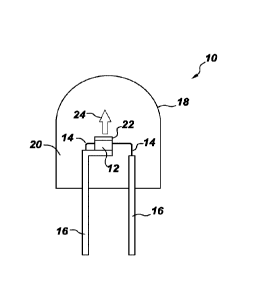
[0026] A lighting apparatus or light emitting assembly or lamp 10 according to
one embodiment of
the present invention is shown in FIG. 1. Lighting apparatus 10 includes a
semiconductor radiation
source, shown as light emitting diode (LED) chip 12, and leads 14 electrically
attached to the LED
chip. The leads 14 may be thin wires supported by a thicker lead frame(s) 16
or the leads may be
self supported electrodes and the lead frame may be omitted. The leads 14
provide current to LED
chip 12 and thus cause it to emit radiation.
[0027] The lamp may include any semiconductor blue or UV light source that is
capable of
producing white light when its emitted radiation is directed onto the
phosphor. In one embodiment,
the semiconductor light source is a blue emitting LED doped with various
impurities. Thus, the
LED may comprise a semiconductor diode based on any suitable III-V, II-VI or
IV-IV semiconductor
layers and having an emission wavelength of about 250 to 550 nm. In
particular, the LED may
contain at least one semiconductor layer comprising GaN, ZnSe or SiC. For
example, the LED
may comprise a nitride compound semiconductor represented by the formula
IniGaiAlkN (where
(N; and I + j + k =1) having an emission wavelength greater than about
250 nm and less
than about 550 nm. In particular embodiments, the chip is a near-uv or blue
emitting LED having a
peak emission wavelength from about 400 to about 500 nm. Such LED
semiconductors are known
in the art. The radiation source is described herein as an LED for
convenience. However, as used
herein, the term is meant to encompass all semiconductor radiation sources
including, e.g.,
semiconductor laser diodes. Further, although the general discussion of the
exemplary structures
of the invention discussed herein is directed toward inorganic LED based light
sources, it should be
understood that the LED chip may be replaced by another radiation source
unless otherwise noted
and that any reference to semiconductor, semiconductor LED, or LED chip is
merely representative
of any appropriate radiation source, including, but not limited to, organic
light emitting diodes.
[0028] In lighting apparatus 10, phosphor composition 22 is radiationally
coupled to the LED chip
12. Radiationally coupled means that the elements are associated with each
other so radiation
from one is transmitted to the other. Phosphor composition 22 is deposited on
the LED 12 by any
appropriate method. For example, a water based suspension of the phosphor(s)
can be formed,
and applied as a phosphor layer to the LED surface. In one such method, a
silicone slurry in which
the phosphor particles are randomly suspended is placed around the LED. This
method is merely
exemplary of possible positions of phosphor composition 22 and LED 12. Thus,
phosphor
- 7 -
CA 02967642 2017-05-11
WO 2016/081340 PCT/US2015/060806
composition 22 may be coated over or directly on the light emitting surface of
the LED chip 12 by
coating and drying the phosphor suspension over the LED chip 12. In the case
of a silicone-based
suspension, the suspension is cured at an appropriate temperature. Both the
shell 18 and the
encapsulant 20 should be transparent to allow white light 24 to be transmitted
through those
elements. Although not intended to be limiting, in some embodiments, the
median particle size of
the phosphor composition ranges from about 1 to about 50 microns, particularly
from about 15 to
about 35 microns.
[0029] In other embodiments, phosphor composition 22 is interspersed within
the encapsulant
material 20, instead of being formed directly on the LED chip 12. The phosphor
(in the form of a
powder) may be interspersed within a single region of the encapsulant material
20 or throughout
the entire volume of the encapsulant material. Blue light emitted by the LED
chip 12 mixes with the
light emitted by phosphor composition 22, and the mixed light appears as white
light. If the
phosphor is to be interspersed within the material of encapsulant 20, then a
phosphor powder may
be added to a polymer or silicone precursor, loaded around the LED chip 12,
and then the polymer
precursor may be cured to solidify the polymer or silicone material. Other
known phosphor
interspersion methods may also be used, such as transfer loading.
[0030] In some embodiments, the encapsulant material 20 is a silicone matrix
having an index of
refraction R, and, in addition to phosphor composition 22, contains a diluent
material having less
than about 5% absorbance and index of refraction of R 0.1. The diluent
material has an index of
refraction of particularly and
more particularly In particular embodiments, the
diluent material is of formula II, and has an index of refraction of about
1.4. Adding an optically
inactive material to the phosphor/silicone mixture may produce a more gradual
distribution of light
flux through the phosphor/encapsulant mixture and can result in less damage to
the phosphor.
Suitable materials for the diluent include fluoride compounds such as LiF,
MgF2, CaF2, SrF2, A1F3,
K2NaAlF6, KMgF3, CaLiAlF6, K2LiAlF6, and K2SiF6, which have index of
refraction ranging from
about 1.38 (AIF3 and K2NaAlF6) to about 1.43 (CaF2), and polymers having index
of refraction
ranging from about 1.254 to about 1.7. Non-limiting examples of polymers
suitable for use as a
diluent include polycarbonates, polyesters, nylons, polyetherimides,
polyetherketones, and
polymers derived from styrene, acrylate, methacrylate, vinyl, vinyl acetate,
ethylene, propylene
oxide, and ethylene oxide monomers, and copolymers thereof, including
halogenated and
unhalogenated derivatives. These polymer powders can be directly incorporated
into silicone
encapsulants before silicone curing.
- 8 -
278858
[0031] In yet another embodiment, phosphor composition 22 is coated onto a
surface of the shell
18, instead of being formed over the LED chip 12. The phosphor composition is
preferably coated
on the inside surface of the shell 18, although the phosphor may be coated on
the outside surface
of the shell, if desired. Phosphor composition 22 may be coated on the entire
surface of the shell
or only a top portion of the surface of the shell. The UV/blue light emitted
by the LED chip 12
mixes with the light emitted by phosphor composition 22, and the mixed light
appears as white
light. Of course, the phosphor may be located in any two or all three
locations or in any other
suitable location, such as separately from the shell or integrated into the
LED.
[0032] FIG. 2 illustrates a second structure of the system according to the
present invention.
Corresponding numbers from FIGS. 1-4 (e.g. 12 in FIG. 1 and 112 in FIG. 2)
relate to
corresponding structures in each of the figures, unless otherwise stated. The
structure of the
embodiment of FIG. 2 is similar to that of FIG. 1, except that the phosphor
composition 122 is
interspersed within the encapsulant material 120, instead of being formed
directly on the LED chip
112. The phosphor (in the form of a powder) may be interspersed within a
single region of the
encapsulant material or throughout the entire volume of the encapsulant
material. Radiation
emitted by the LED chip 112 mixes with the light emitted by the phosphor 122,
and the mixed light
appears as white light 124. If the phosphor is to be interspersed within the
encapsulant material
120, then a phosphor powder may be added to a polymer precursor, and loaded
around the LED
chip 112. The polymer or silicone precursor may then be cured to solidify the
polymer or silicone.
Other known phosphor interspersion methods may also be used, such as transfer
molding.
[0033] FIG. 3 illustrates a third possible structure of the system according
to the present
invention. The structure of the embodiment shown in FIG. 3 is similar to that
of FIG. 1, except that
the phosphor composition 222 is coated onto a surface of the envelope 218,
instead of being
formed over the LED chip 212. The phosphor composition 222 is preferably
coated on the inside
surface of the envelope 218, although the phosphor may be coated on the
outside surface of the
envelope, if desired. The phosphor composition 222 may be coated on the entire
surface of the
envelope, or only a top portion of the surface of the envelope. The radiation
226 emitted by the
LED chip 212 mixes with the light emitted by the phosphor composition 222, and
the mixed light
appears as white light 224. Of course, the structures of FIGS. 1-3 may be
combined, and the
phosphor may be located in any two or all three locations, or in any other
suitable location, such as
separately from the envelope, or integrated into the LED.
- 9 -
Date Recue/Date Received 2022-02-04
CA 02967642 2017-05-11
WO 2016/081340 PCT/US2015/060806
[0034] In any of the above structures, the lamp may also include a
plurality of scattering
particles (not shown), which are embedded in the encapsulant material. The
scattering particles
may comprise, for example, alumina or titania. The scattering particles
effectively scatter the
directional light emitted from the LED chip, preferably with a negligible
amount of absorption.
[0035] As shown in a fourth structure in FIG. 4, the LED chip 412 may be
mounted in a
reflective cup 430. The cup 430 may be made from or coated with a dielectric
material, such as
alumina, titania, or other dielectric powders known in the art, or be coated
by a reflective metal,
such as aluminum or silver. The remainder of the structure of the embodiment
of FIG. 4 is the
same as those of any of the previous figures, and can include two leads 416, a
conducting wire
432, and an encapsulant material 420. The reflective cup 430 is supported by
the first lead 416
and the conducting wire 432 is used to electrically connect the LED chip 412
with the second
lead 416.
[0036] Another structure (particularly for backlight applications) is a
surface mounted device
("SMD") type light emitting diode 550, e.g. as illustrated in FIG. 5. This SMD
is a "side-emitting
type" and has a light-emitting window 552 on a protruding portion of a light
guiding member 554.
An SMD package may comprise an LED chip as defined above, and a phosphor
material that is
excited by the light emitted from the LED chip. Other backlight devices
include, but are not limited
to, TVs, computers, smartphones, tablet computers and other handheld devices
that have a
display including a semiconductor light source; and a color stable Mn4+ doped
phosphor according
to the present invention.
[0037] When used with an LED emitting at from 350 to 550 nm and one or more
other appropriate
phosphors, the resulting lighting system will produce a light having a white
color. Lamp 10 may
also include scattering particles (not shown), which are embedded in the
encapsulant material.
The scattering particles may comprise, for example, alumina or titania. The
scattering particles
effectively scatter the directional light emitted from the LED chip,
preferably with a negligible
amount of absorption.
[0038] In addition to the color stable Mn4+ doped phosphor, phosphor
composition 22 may include
one or more other phosphors. When used in a lighting apparatus in combination
with a blue or
near UV LED emitting radiation in the range of about 250 to 550 nm, the
resultant light emitted by
the assembly will be a white light. Other phosphors such as green, blue,
yellow, red, orange, or
other color phosphors may be used in the blend to customize the white color of
the resulting light
- 10-
CA 02967642 2017-05-11
WO 2016/081340 PCT/US2015/060806
and produce specific spectral power distributions. Other materials suitable
for use in phosphor
compostion 22 include electroluminescent polymers such as polyfluorenes,
preferably poly(9,9-
dioctyl fluorene) and copolymers thereof, such as poly(9,9'-dioctylfluorene-co-
bis-N,N'-(4-
butylphenyl)diphenylamine) (F8-TFB); poly(vinylcarbazole) and
polyphenylenevinylene and their
derivatives. In addition, the light emitting layer may include a blue, yellow,
orange, green or red
phosphorescent dye or metal complex, or a combination thereof. Materials
suitable for use as the
phosphorescent dye include, but are not limited to, tris(1-phenylisoquinoline)
iridium (III) (red dye),
tris(2-phenylpyridine) iridium (green dye) and Iridium (III) bis(2-(4,6-
difluorephenyl)pyridinato-N,C2)
(blue dye). Commercially available fluorescent and phosphorescent metal
complexes from ADS
(American Dyes Source, Inc.) may also be used. ADS green dyes include
ADS060GE,
ADS061GE, ADS063GE, and ADS066GE, ADS078GE, and ADS090GE. ADS blue dyes
include
ADS064BE, ADS065BE, and ADS070BE. ADS red dyes include ADS067RE, ADS068RE,
ADS069RE, ADS075RE, ADS076RE, ADS067RE, and ADS077RE.
[0039] Suitable phosphors for use in phosphor composition 22 in addition to
the Mn4+ doped
phosphor include, but are not limited to:
((Sri (Ca, Ba, Mg, Zn)z),Hx+w)( Li, Na, K, Rb)wCex)3(Ali_ySiy)04-,y+3(x-w)Fi-y-
3(6-w), 0<x5Ø10, 0545Ø5,
1211Atx; (Ca, Ce)3Sc2Si3012 (CaSiG);
(Sr,Ca,Ba)3Ali_xSix04,-xFi_x:Ce3+ (SASOF));
(Ba,Sr,Ca)5(PO4)3(CI,F,Br,OH):Eu2+,Mn2+; (Ba,Sr,Ca)BP05:Eu2+,Mn2+;
(Sr,Ca)10(PO4)6*vB203:Eu2+
(wherein 0<v..1); Sr2Si308*2SrC12:Eu2+; (Ca,Sr,Ba)3MgSi208:Eu2+,Mn2+;
BaA18013:Eu2+;
2SrO*0.84P205*0.1 613203: Eu2'; (Ba,Sr,Ca)MgAl1c,017:Eu2 ,Mn2+;
(Ba,Sr,Ca)A1204:Eu2+;
(Y,Gd,Lu,Sc,La)B03:Ce3+,Tb3+; ZnS:Cu+,Cr; ZnS:Cu+,A13+; ZnS:Ag+,Cr;
ZnS:Ag+,A13+;
(Ba,Sr,Ca)2Si1-04-24:Eu2+
(wherein -0.20.2); (Ba,Sr,Ca)2(Mg,Zn)Si207:Eu2+; (Sr,Ca,Ba)(AI,Ga,ln)2S4:Eu2+;
(Y,Gd,Tb,La,Sm,Pr,Lu)3(AI,Ga)5,012-3/2.:Ce3+ (wherein 0c(,0.5);
(Y,Gd,Lu,Tb)3(AI,Ga)5012:Ce3+;
(Ca,Sr)8(Mg,Zn)(SiO4)4C12:Eu2+,Mn2+; Na2Gd2B207:Ce3+,Tb3+;
(Sr,Ca,Ba,Mg,Zn)2P207:Eu2+,Mn2+;
(Gd,Y,Lu,La)203:Eu3+,Bi3+; (Gd,Y,Lu,La)202S:Eu3+,Bi3+;
(Gd,Y,Lu,La)VO4:Eu3+,Bi3+;
(Ca,Sr)S:Eu2+,Ce3+; SrY2S4:Eu2+; CaLa2S4:Ce3+; (Ba,Sr,Ca)MgP207:Eu2+,Mn2+;
(Y,Lu)2W06:Eu3+,Mo6 ; (Ba,Sr,Ca)13Si1N,:Eu2+ (wherein 2[3+47=30;
(Ba,Sr,Ca)2Si5.xAlxN8_,<Ox:Eu2+ (wherein 0)(2); Ca3(S104)C12:Eu2+;
(Lu,Sc,Y,Tb)2_,,,_,CevCaii-ul-lwMg2_,,P,,(Si,Ge)3012-u/2 (where -0.5u1,
0<v0.1, and 0vv0.2);
(Y,Lu,Gd)2_,CawSi4N6+,C1,:Ce3+, (wherein 0(.p0.5); (Lu,Ca,Li,Mg,Y)
-11-
CA 02967642 2017-05-11
WO 2016/081340 PCT/US2015/060806
a-SiAION doped with Eu2+ and/or Ce3+; (Ca,Sr,Ba)SiO2N2:Eu2+,Ce3+;
13-SiAION:Eu2+, 3.5MgO*0.5MgF2*Ge02:Mn4+; (Sr,Ca,Ba,Mg)AlSiN3:Eu2+;
(Sr,Ca,Ba)3Si05:Eu2+; Cai_c4CecEufAli+cSii_cN3, (where 0c0.2, 00.2);
CalCehEurAli_h(Mg,Zn)hSiN3, (where 051-150.2, 05r50.2);
Ca1-23-tCe5(Li,Na)5EutAlSiN3 (where (:)s0.2, si-t>0); and
Ca1.,,_0Ce,(Li,Na),Eu0A11+Sii,N3, (where 0cy0.2, 000.2).
[0040] In particular, phosphor composition 22 may include one or more
phosphors that result in a
green spectral power distribution under ultraviolet, violet, or blue
excitation. In the context of the
present invention, this is referred to as a green phosphor or green phosphor
material. The green
phosphor may be a single composition or a blend that emits light in a green to
yellow-green to
yellow range, such as cerium-doped yttrium aluminum garnets, more particularly
(Y,Gd,Lu,Tb)3(AI,Ga)5012:Ce3+. The green phosphor may also be a blend of blue-
and red-shifted
garnet materials. For example, a Ce3+-doped garnet having blue shifted
emission may be used in
combination with a Ce3+-doped garnet that has red-shifted emission, resulting
in a blend having a
green spectral power distribution. Blue- and red-shifted garnets are known in
the art. In some
embodiments, versus a baseline Y3A15012:Ce3+ phosphor, a blue-shifted garnet
may have Lu3+
substitution for Y3', Ga3+ substitution for A13% or lower Ce3+ doping levels
in a Y3A15012:Ce3+
phosphor composition. A red-shifted garnet may have Gd3+/Tb3+ substitution for
Y3+ or higher Ce3+
doping levels.
[0041] The ratio of each of the individual phosphors in the phosphor blend may
vary depending on
the characteristics of the desired light output. The relative proportions of
the individual phosphors
in the various embodiment phosphor blends may be adjusted such that when their
emissions are
blended and employed in an LED lighting device, there is produced visible
light of predetermined x
and y values on the CIE chromaticity diagram. As stated, a white light is
preferably produced. This
white light may, for instance, may possess an x value in the range of about
0.20 to about 0.55, and
a y value in the range of about 0.20 to about 0.55. As stated, however, the
exact identity and
amounts of each phosphor in the phosphor composition can be varied according
to the needs of
the end user. For example, the material can be used for LEDs intended for
liquid crystal display
(LCD) backlighting. In this application, the LED color point would be
appropriately tuned based
upon the desired white, red, green, and blue colors after passing through an
LCD/color filter
combination. The list of potential phosphor for blending given here is not
meant to be exhaustive
- 12 -
CA 02967642 2017-05-11
WO 2016/081340 PCT/US2015/060806
and these Me-doped phosphors can be blended with various phosphors with
different emission to
achieve desired spectral power distributions.
[0042] In some embodiments, lighting apparatus 10 has a color temperature less
than or equal to
4200 K, and phosphor composition 22 includes a red phosphor consisting of a
color stable Me
doped phosphor of formula I. That is, the only red phosphor present in
phosphor composition 22 is
the color stable Mn4+ doped phosphor; in particular, the phosphor is
K2SiF6:Mn4+. The composition
may additionally include a green phosphor. The green phosphor may be a Ce3+-
doped garnet or
blend of garnets, particularly a Ce3+-doped yttrium aluminum garnet, and more
particularly, YAG
having the formula (Y,Gd,Lu,Tb)3(AI,Ga)5012:Ce3+. When the red phosphor is
K2SiF6:Mn4+, the
mass ratio of the red phosphor to the green phosphor material may be less than
3.3, which may be
significantly lower than for red phosphors of similar composition, but having
lower levels of the Mn
dopant.
[0043] LED devices incorporating the color stable phosphors and used for
backlighting or general
illumination lighting may have a color shift of <1.5 MacAdam ellipses over
2,000 hours of device
operation, and, in particular embodiments, <1 MacAdam ellipse over 2,000
hours, where the
phosphor/polymer composite is in direct contact with the LED chip surface, LED
wall plug efficiency
greater than 40%,and LED current densities are greater than 2 A/cm2. In
accelerated testing,
where the phosphor/polymer composite is in direct contact with the LED chip
surface, LED wall
plug efficiency greater than 18%, and LED current densities are greater than
70 A/cm2, LED
devices may have color shift of <1.5 MacAdam ellipse over 30 minutes.
[0044] The color stable Me doped phosphors of the present invention may be
used in
applications other than those described above. For example, the material may
be used as a
phosphor in a fluorescent lamp, in a cathode ray tube, in a plasma display
device or in a liquid
crystal display (LCD). The material may also be used as a scintillator in an
electromagnetic
calorimeter, in a gamma ray camera, in a computed tomography scanner or in a
laser. These uses
are merely exemplary and not limiting.
EXAMPLES
General Procedures
Silicone Tape Sample Preparation
- 13-
278858
[0045] Samples were prepared by mixing 500 mg of the material to be tested
with 1.50 g silicone
(SylgardTM 184). The mixture was degassed in a vacuum chamber for about 15
minutes. The
mixture (0.70 g) was poured into a disc-shaped template (28.7mm diameter and
0.79 mm thick)
and baked for 30 minutes at 90 C. The sample was cut into squares of size
approximately 5 mm x
mm for testing.
Stability Testing
High Light Flux Conditions
[0046] A laser diode emitting at 446 nm was coupled to an optical fiber with a
collimator at its other
end. The power output was 310 mW and the beam diameter at the sample was 700
microns. This
is equivalent to a flux of 80 W/cm2 on the sample surface. The spectral power
distribution (SPD)
spectrum that is a combination of the scattered radiation from the laser and
the emission from the
excited phosphor is collected with a 1 meter (diameter) integrating sphere and
the data processed
with the spectrometer software (Specwin). At intervals of two minutes, the
integrated power from
the laser and the phosphor emission were recorded over a period of about 21
hours by integrating
the SPD from 400nm to 500nm and 550 nm to 700 nm respectively. The first 90
minutes of the
measurement are discarded to avoid effects due to the thermal stabilization of
the laser. The
percentage of intensity loss due to laser damage is calculated as follows:
(Power ¨ Initial power)
Intensity loss (%) = 100 ________________________________
Initial power
While only the emitter power from the phosphor is plotted, the integrated
power from the
laser emission as well as its peak position was monitored to ensure that the
laser remained
stable (variations of less than 1%) during the experiment.
High Temperature High Humidity (HHTH) Treatment
[0047] Samples for high temperature, high humidity (HTHH) treatment were made
by mixing
phosphor powders into a two-part methyl silicone binder (RTV-615, Momentive
Performance
Materials) in a ratio of 0.9 g phosphor to 0.825 g silicone (parts A+B). The
phosphor/silicone
mixture is then poured into aluminum sample holders and cured at 90 C for 20
minutes. Control
samples were stored under nitrogen, and samples for exposure to HTHH
conditions were placed
into a 85 C/85% RH controlled atmosphere chamber. These HTHH samples are
periodically
- 14 -
Date Recue/Date Received 2022-02-04
CA 02967642 2017-05-11
WO 2016/081340 PCT/US2015/060806
removed and their luminescence intensity under 450 nm excitation compared to
that of the control
samples.
Relative Brightness
[0048] A phosphor tape containing 25 wt% phosphor, VA" wide and 1/32" thick,
is prepared
according to the procedure above. The tape is placed within an integrating
sphere about 1/2 "
away from the LED and held in place by a cylindrical spacer coated with a
highly reflective film.
Emission intensity was measured at wavelengths ranging between 550 nm and 700
nm, integrated
and normalized to emission of a reference sample composed of a commercial
K2SiF6:Mn4+ material
containing 0.7 weight % Mn, obtained from ShinEtsu Chemicals.
EXAMPLES 1-4 Preparation of K2SiF6:Mn4+ with manganese levels ranging from
0.91 wt% to
1.19 wt%
[0049] Amounts and distribution of starting materials among Beakers A-D are
shown in Table 1.
For Example 4, 5 mL of acetone was also added to beaker B. Procedure: Beaker A
was stirred
aggressively, and the contents of beaker B were added dropwise at a rate of 75
mL/min for 30
seconds and then 60 mL/min for the remainder of the reaction. The contents of
beaker D were
added dropwise to beaker A at a rate of 13 mL/minute 20 seconds after the
contents of beaker B
began to be added. The contents of beaker C were added dropwise to beaker A at
a rate of 13
mL/minute 30 seconds after the contents of beaker B began to be added. The
precipitate was
digested for 5 minutes and the stirring was stopped. The supernatant was
decanted, and the
precipitate was vacuum filtered, rinsed once with acetic acid and twice with
acetone, and then
dried under vacuum. The dried powder was sifted through 44 micron mesh, and
annealed under
20% F2 for 8hr. at 540 C. The annealed phosphor was washed in a solution of
49% HF saturated
with K2SiF6, dried under vacuum and sifted.
[0050] The amount of manganese incorporated in the phosphor was determined by
inductively
coupled plasma mass spectrometry (ICP-MS), and is reported as weight %, based
on total weight
of the phosphor material.
Table 1
Source KF (g) K2MnF6 (g) 35% H2SiF6 (mL) 49% HF (mL)
Example 1: 0.91% Mn
- 15-
CA 02967642 2017-05-11
WO 2016/081340 PCT/US2015/060806
Table 1
Source KF (g) K2MnF6 (g) 35%
H2SiF6 (mL) 49% HF (mL)
Beaker A 19g 1.19 100
Beaker B 47.3 150
Beaker C 1.45 25
Beaker D 8.9 20
Example 2: 1.19% Mn
Beaker A 19 0.88 90
Beaker B 46.8 148
Beaker C 2.04 35
Beaker D 8.9 20
Example 3: 1.17% Mn
Beaker A 14 0.88 85
Beaker B 46.6 147
Beaker C 2.0 30
Beaker D 14 28
Example 4: 0.94% Mn
Beaker A 10 0.88 80
Beaker B 46.6 147
Beaker C 2.0 30
Beaker D 14 28
[0051] Samples were evaluated for laser damage, quantum efficiency (reported
as relative QE,
setting the value of QE of a reference material composed of commercial
K2SiF6:Mn4+ containing
0.7 weight % Mn, obtained from ShinEtsu Chemicals, to 100%) and absorbance at
450 nm.
Results are shown in Table 2. It can be seen that laser damage was lower, and
QE and
absorbance were higher compared to the commercial control.
Table 2
Example No. Laser Damage QE
(relative) Abs 450nm wt %Mn
Control 7.2% 100.0% 68.8% 0.73%
1 1.0% 103.0% 74.0% 0.91%
2 2.7% 103.6% 80.1% 1.19%
- 16-
CA 02967642 2017-05-11
WO 2016/081340
PCT/US2015/060806
Table 2
Example No. Laser Damage QE (relative) Abs 450nm wt %Mn
3 1.3% 101.6% 75.3% 1.17%
4 1.5% 103.3% 73.0% 0.94%
COMPARATIVE EXAMPLE 1
[0052] Mn-doped potassium fluorosilicate, containing 0.84 wt% Mn, based on
total weight of the
material, was annealed I a furnace at 540 C under an atmosphere containing
20`)/0F2/80%N2 at 10
psia for 8 hours. The annealed phosphor was washed in a solution of 49% HF
saturated with
K2SiF6, dried under vacuum and sifted. The phosphor and an annealed, untreated
commercial
sample were tested under conditions of high light flux. Results are shown in
Table 3.
TABLE 3
Laser Relative
Example No. Damage QE, % %Mn Conditions
Control 10.9% 100 0.84% No treatment
Comp. Ex. 1 1.5% 107.5 0.82% 540 C,
20%F2/80%N2, 10 psia, 8 hours
EXAMPLES 5 and 6 Properties of K2SiF6:Mn4+ with 0.9 wt% and 1.25 wt% manganese
[0053] Mn-doped potassium fluorosilicate materials were prepared and treated
as in Examples 1-
4. Quantum efficiency and decay time were measured and weight % Mn was
determined by ICP-
MS, before and after treatment. Results are shown in Table 4. It can be seen
that the quantum
efficiency of high Mn samples was improved, and the onset/effects of
concentration quenching
were reduced. The improvement in QE at least is significantly greater than
that observed at lower
Mn levels. For example, QE of the phosphor of Comparative Example 1, having
0.84 wt% Mn,
increased from 100 (relative) to 107 (relative), about 7% increase, while the
increase shown in
Table 4 is about 15% for the sample containing 0.9 wt% Mn, and about 20% for
the sample
containing 1.25 wt% Mn.
Table 4
Example No. QE (relative) Decay time Mn level (wt%)
Notes
90 8.19 ms 0.94% Before treatment
104.5 8.70 ms 0.90% After
treatment
6 80 7.95 ms 1.39% Before treatment
103 8.69 ms 1.25% After
treatment
- 17-
CA 02967642 2017-05-11
WO 2016/081340
PCT/US2015/060806
COMPARATIVE EXAMPLE 2
[0054] A commercial K2SiF6:Mn4+ phosphor with a manganese content of 0.70% (as
determined by
Induced Coupled Plasma) was placed in a furnace under a nitrogen (80%) and
fluorine (20%)
atmosphere at 10 psia and heated at 540 C for 8 hours. After 8 hours, the
temperature was
decreased at a rate of 10 C per minute. The annealed phosphor was washed in a
solution of 49%
HF saturated with K2SiF6, dried under vacuum and sifted.
EXAMPLE 7 Slow Cooling After Annealing
[0055] A commercial K2SiF6:Mn4+ phosphor with a manganese content of 0.70% (as
determined by
Induced Coupled Plasma) was placed in furnace under a nitrogen (80%) and
fluorine (20%)
atmosphere at 10 psia and heated at 540 C for 8 hours. After 8 hours, the
temperature was
decreased at a rate of 1 C per minute. The annealed phosphor was washed in a
solution of 49%
HF saturated with K2SiF6, dried under vacuum and sifted.
[0056] Stability of the phosphors of Comparative Example 2 and Example 7 was
evaluated and
compared to the untreated commercial control having manganese content of
0.70%. Annealing
improved stability, and using a slow cool down further decreased % intensity
loss.
EXAMPLES 8-23 K2SiF6:Mn4 with manganese levels ranging from 1.1 wt% to 5.3
wt%
COMPARATIVE EXAMPLES 3-5 K2SiF6:Mn4+ with manganese levels ranging from 0.52
wt% to
0.79 wt%
[0057] Mn-doped potassium fluorosilicate materials were prepared and post
treated as in
Examples 1-4, except that the amounts of raw materials were adjusted according
to the higher
levels of manganese. Relative quantum efficiency, emission decay lifetime and
brightness were
measured for the products before and after the post treatment. Results are
shown in Table 5.
Table 5
Before After
Comp. Ex. [Me], Relative Relative Lifetime, Relative Relative Lifetime,
Ex. No. wt% QE, Brightness, ms QE, Brightness, ms
No.
1 0.52 92 88 104 95 8.6
2 0.7 98 8.4 106 110 8.6
3 0.79 97 106 8.4 106 117 8.6
- 18-
CA 02967642 2017-05-11
WO 2016/081340
PCT/US2015/060806
Table 5
Before After
Comp. Ex. [Mn4], Relative Relative Lifetime, Relative Relative Lifetime,
Ex. No. wt% QE, Brightness, ms QE, Brightness, ms
No. % % % %
8 1.1 103 134 8.6
9 1.4 89 122 8.0 104 140 8.6
2.1 83 124 7.7 102 151 8.5
11 2.6 69 108 7.2 101 154 8.5
12 2.7 76 123 98 156 8.5
13 2.9 65 105 7.2 97 158 8.5
14 3.0 72 110 7.1 105 163 8.4
3.2 59 93 7.3 89 137 8.2
16 3.4 60 95 6.8 98 155 8.4
17 3.4 51 85 6.8 95 153 8.4
18 3.5 53 85 6.9 91 143 8.3
19 3.6 53 87 7.0 88 141 8.2
3.9 30 53 6.3 67 116 7.8
21 4.0 42 69 6.7 82 135 8.1
_ 22 4.4 17 29 7.9 36 61 6.8
-
23 5.3 7 11 4.3 31 53 7.0
[0058] Untreated samples had a relative QE lower than 90% at Mn4+
concentrations over 1% due
to concentration quenching. The range at which the QE remained high was
extended to at least 3
wt% by post treatment, and lifetime was greater than 8.4 ms to about 3.4 wt%.
The significant
improvement in properties resulting from the post treatment extended to about
4 wt%.
EXAMPLE 24 K2SiF6:Mn4+ blends with color temperature of 3000 K
[0059] The Mn-doped potassium fluorosilicate materials of Examples 2, 3 and 10
were blended
with YAG and tapes were prepared to emit light having a color temperature of
3000 K.
Composition of the blends is shown in Table 6.
Table 6
Blend Composition
Red phosphor YAG, %wt.
Silicone, %wt.
Example [Mn4+],
%
Wt
No. wt% ,
2 0.70% 20.8% 5.2% 74.0%
3 0.79% 18.6% 5.4% 76.0%
- 19-
CA 02967642 2017-05-11
WO 2016/081340 PCT/US2015/060806
Table 6
Blend Composition
Red phosphor YAG, %wt. Silicone, %wt.
Example [Mn4+],
Wt, 0/0
No. wt%
2.05% 8.4% 6.0% 85.6%
[0060] It can be seen that significantly less of the red phosphor material
with higher Mn
concentration was used, compared to the materials having lower Mn
concentration.
[0061] While only certain features of the invention have been illustrated and
described herein,
many modifications and changes will occur to those skilled in the art. It is,
therefore, to be
understood that the appended claims are intended to cover all such
modifications and changes as
fall within the true spirit of the invention.
- 20 -