Note: Descriptions are shown in the official language in which they were submitted.
CA 02968079 2017-05-16
WO 2016/09902
PCT/US2015/054602
SURFACE MOUNT BATTERY AND PORTABLE ELECTRONIC DEVICE WITH
INTEGRATED BATTERY CELL
Technical Field
[0001] This disclosure relates to surface mount batteries for electronic
devices.
Background
[0002] Electronic devices, including mobile platforms such as smartphones,
laptops, notebook computers, and tablet computers, continue to shrink in size.
A
power delivery system, including one or more battery cells, is often among the
largest components of a portable electronic device. As portable electronic
devices
shrink in size, users also expect that power delivery systems will grow
smaller and
more portable. Integration of batteries into physically small systems, and
particularly thin systems, presents a challenge when plugs, sockets and even
tabs are used to connect batteries to the systems.
Brief Description of the Drawings
[0003] Arrangements and embodiments may be described in detail with reference
to the following drawings, in which like reference numerals refer to like
elements and
wherein:
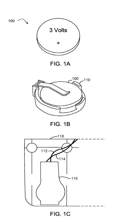
[0004] FIGS. 1A, 1B, and 1C, illustrate an example coin shape Li-ion
battery that
uses a liquid electrolyte.
[0005] FIG. 2 is a perspective view of a battery cell including solid
electrolytes
according to one embodiment.
[0006] FIG. 3 is a side view of a circuit board assembly according to one
embodiment.
[0007] FIGS. 4A, 4B, 4C, and 4D illustrate a mobile electronic device
including an
integrated solid electrolyte battery according to one embodiment.
[0008] FIG. 5 is a cross-sectional side view of a circuit board including
an
integrated battery cell according to one embodiment.
[0009] FIG. 6 is a cross-sectional side view of a battery cell according to
one
embodiment.
[0010] FIG. 7 is flow chart of a method for manufacturing a circuit board
according to one embodiment.
[0011] FIG. 8 is a flow chart of a method for manufacturing a circuit board
according to another embodiment.
1
CA 02968079 2017-05-16
WO 2016/099632
PCT/US2015/054602
Detailed Description of Embodiments
[0012] Embodiments and arrangements disclosed herein use battery cells
including solid electrolytes, such as solid polymers or ceramics. Unlike
batteries with
liquid electrolytes, batteries with solid polymer and/or ceramic electrolytes
can
withstand the high temperatures and durations of reflow solder processes that
may be used for surface-mountable batteries and open new assembly options.
Solid electrolyte cell batteries are also safer than liquid electrolyte cell
batteries,
as discussed below, since a flammable liquid electrolyte has the been a cause
of catastrophic failures of common lithium-ion (Li-ion) batteries. Certain
embodiments disclosed herein provide space savings, lower assembly costs,
size reduction (e.g., in an X-Y plane), and/or height reduction (e.g., in a Z
direction perpendicular to the X-Y plane). In addition, or in other
embodiments,
disclosed systems and methods may provide for direct integration of a battery
in
a system, removing much of the overhead of packaging and socket use. In
certain embodiments, the solid electrolyte battery cells disclosed herein are
rechargeable.
[0013] Small size batteries commercially available for surface mounting in
handheld or portable electronic devices have a low capacity (e.g., liquid
electrolyte cell batteries) or extremely low capacity (e.g., solid-state thin-
film
batteries). Small size secondary batteries have been used as power sources for
memory backup of portable equipment such as cellular phones in recent years.
For
example, FIGS. 1A, 1B, and 1C, illustrate a coin shape Li-ion battery 100 that
uses a
liquid electrolyte and is packaged in a rigid, hermetically sealed metal "can"
housing.
The process of canning and hermetically sealing the coin shape Li-ion battery
100
may be costly and complex. Further, the can housing limits energy density,
particularly in multi-cell packs where placing cylindrical cells side by side
creates
gaps of empty space. The coin shape Li-ion battery 100 may have a positive
electrode including a lithium manganese composite oxide and a negative
electrode
including a lithium aluminum alloy and having a voltage of approximately 3V.
As
another example, a coin shape lithium secondary battery with a positive
electrode
including niobium pentoxide and a negative electrode including a lithium
aluminum
alloy and having a voltage of approximately 2.5 V has been used.
[0014] A problem with lithium batteries, such as that shown in FIG. 1A, is
that
liquid electrolyte is extremely flammable. Thus, soldering the coin shape Li-
ion
2
CA 02968079 2017-05-16
WO 2016/099632
PCT/US2015/054602
battery 100 to a circuit board may be dangerous. As one example of a reflow
method, soldering is carried out by supplying solder between a circuit board
and a
terminal of a part, and then allowing the circuit board and the part to pass
through a
high temperature atmosphere. The soldering ensures an electrical contact
between
a circuit on the circuit board and the terminal of the part. The high
temperature
atmosphere may range, for example from about 220 C to about 260 C, depending
on the materials and processes used. Such conditions can cause high pressure
to
build within the can housing of the coin shape Li-ion battery 100 such that it
either
vents electrolyte or explodes. In a high temperature atmosphere, the
electrolyte can
flame as it is vented. Attempts to make the volatile liquid electrolyte less
flammable
to allow for surface-mount coin cells, have generally resulted in battery
cells with
very low capacities (e.g., up to about 2.5 mAh).
[0015] Thus, many applications avoid soldering Li-ion batteries with a
liquid
electrolyte to a circuit board. Rather, as shown in FIG. 1B, the coin shape Li-
ion
battery 100 may be placed in a holder 110 that has previously been soldered to
a
circuit board. The bulky holder 110 may add additional size and expense to the
overall electronic device. In another example, as shown in FIG. 1C, the coin
shape
Li-ion battery 100 may be located remote from the circuit board and
electrically
connected thereto via wires 112, 114. Such implementations may add expense,
for
example, by manually soldering wires to the coin shape Li-ion battery 100,
inserting
the coin shape Li-ion battery 100 in a shrink wrap cover 116, applying heat to
shrink
the shrink wrap cover, soldering the other end of the wires 112, 114 to the
circuit
board, and gluing or otherwise attaching the shrink wrap cover 116 to a
chassis 118
of the electronic device.
[0016] To avoid the problems with liquid electrolytes, certain embodiments
disclosed herein use solid electrolytes. For example, FIG. 2 is a perspective
view of
a battery cell 200 including solid electrolytes 210 according to one
embodiment. The
solid electrolytes 210 may include a solid electrolyte cathode material
electrically
coupled to a first electrode 212 and a solid electrolyte anode material
electrically
coupled to a second electrode 214. The solid electrolyte cathode material and
the
solid electrolyte anode material may each include, for example, a solid
polymer or
ceramic material. The solid electrolyte anode material may comprise, for
example,
graphite, silicon, or a blend of graphite and silicon. The solid electrolyte
cathode
material may comprise, for example, a lithium metal oxide, such as lithium
cobalt
3
CA 02968079 2017-05-16
WO 2016/0996.32
PCT/US2015/054602
oxide (LCO) or nickel cobalt aluminum (NCA). Such materials may be used for
any
of the anodes and/or cathodes disclosed herein (i.e., not just for the
embodiment
shown in FIG. 2). Further a solid polymer separator or ceramic separator may
separate the solid electrolyte cathode material from the solid electrolyte
anode
material, to prevent electrical short circuits and allow for the transport of
ionic charge
carriers during the passage of current in the battery cell 200. The first
electrode 212
and the second electrode 214 are electrically conductive and include a
material (e.g.,
copper, silver, or aluminum) that can be soldered to an electrically
conductive trace
on a printed circuit board or other substrate. In certain embodiments, a
plastic or
other laminate material may cover the solid electrolytes 210.
[0017] The battery
cell 200 including the solid electrolytes 210 may be selectively
sized, shaped, and configured for a particular surface mounting application.
As
shown in FIG. 2, the battery cell 200 may be rectangular, for example, to fit
on a
crowded circuit board. However, persons skilled in the art will recognize from
the
disclosure herein that the all-solid construction allows the battery cell 200
to have
any rectangular or non-rectangular shape. Further, because there is no liquid
that
has to be contained by a hermetically sealed, rigid metal can, the height,
width and
length of the battery cell 200 can be selected to meet electrical storage
capacity and
space needs. Further, cost is reduced by avoiding the canning and sealing
process,
and the battery cell is safer that liquid electrolyte cells because the solid
electrolytes
210 cannot leak or vent. The solid electrolytes 210 can also withstand extreme
environmental conditions, such as the high temperatures associated with reflow
soldering techniques.
[0018] FIG. 3 is a side view of a circuit board assembly 300 according to
one
embodiment. The circuit board assembly 300 includes a metal layer 310 over a
non-
conductive substrate 312. The metal layer 310 may include, for example, copper
or
other electrically conductive materials. Although not shown in FIG. 3, certain
embodiments may include another metal layer below the non-conductive substrate
312 (e.g., used as a ground plane or power plane) connected to the top metal
layer
310 through plated vias in the non-conductive substrate 312). The non-
conductive
substrate 312 may include, for example, fiberglass or non-conductive
laminates.
[0019] During the
manufacturing process, the metal layer 310 may be etched or
otherwise formed to create a trace pattern for electrically connecting a
plurality of
circuit components 314, 316. The circuit components 314, 316 may include, for
4
CA 02968079 2017-05-16
WO 2016/099632
PCT/US2015/054602
example, capacitors, resistors, transistors, and/or processors or other
integrated
circuits. As shown in FIG. 3, the battery cell 200 of FIG. 2 may be soldered
onto the
trace of the metal layer 310 along with the other circuit components 314, 316
of the
circuit board assembly 300. Using automated processes (e.g., pick-and-place
machines and/or reflow soldering) to populate the circuit board assembly 300
with
the battery cell 200 along with the other components 314, 316 reduces manual
labor
and the overall cost of manufacturing the circuit board assembly 300.
[0020] FIGS. 4A, 4B, 4C, and 4D illustrate a mobile electronic device 400
including an integrated solid electrolyte battery according to one embodiment.
FIG.
4A shows a perspective view of the mobile electronic device 400 being handled
by a
user 402. In this example, the mobile electronic device 400 is a tablet
computer.
However, in other embodiments any mobile device may be used, such as a
smartphone, a laptop computer, a notebook computer, a personal digital
assistant
(PDA), an audio and/or video player, a gaming device, a camera, a wearable
device
(e.g., an exercise or health monitor), or any other device using electrical
power. As
shown in FIG. 4A, the mobile electronic device 400 may include a chassis 410
for
enclosing electronic circuitry and other components, and a display screen 412
to
interface with the user 402. The display screen 412 may be a liquid crystal
display
(LCD) screen or other type of display screen, such as an organic light
emitting diode
(OLED) display. The display screen 412 can be configured as a touch screen.
The
touch screen may use capacitive, resistive, or another type of touch screen
technology.
[0021] Those skilled in the art will also recognize from the disclosure
herein that
the mobile electronic device 400 may include a variety of additional
components.
For example, the mobile electronic device 400 may include one or more antennas
configured to communicate with a transmission station, such as a base station
(e.g.,
of a cellular network), a base band unit, a remote radio head, a remote radio
equipment, a relay station, a radio equipment, or another type of wireless
wide area
network (VVWAN) access point. As further examples, the mobile electronic
device
400 may also include a microphone and one or more speakers that can be used
for
audio input and output from the mobile electronic device 400, an application
processor (e.g., configured to perform the functions described herein), a
graphics
processor coupled to internal memory to provide processing and display
capabilities,
a non-volatile memory port to provide data input/output options to the 402
user
CA 02968079 2017-05-16
WO 2016/09902
PCT/US2015/054602
and/or to expand the memory capabilities of the mobile electronic device 400,
a
keyboard (e.g., integrated with the mobile electronic device 400 or wirelessly
connected to the mobile electronic device 400) to provide additional user
input,
and/or a virtual keyboard provided using the touch screen.
[0022] FIG. 46 illustrates a side view of the mobile electronic device 400.
In this
example, the chassis 410 of the mobile electronic device 400 includes a back
plate
414. At least a portion of the back plate 414 is electrically conductive. For
example,
the back plate 414 may comprise aluminum. FIG. 4C illustrates an inside
surface
416 of the back plate 414 (e.g., an internal surface of mobile electronic
device 400
when assembled). The inside surface 416 may include structural elements 418
(e.g., strengthening ribs, walls or guides) to provide structural support to
the chassis.
However, as shown in FIG. 4C, the inside surface 416 of the back plate 414 may
include large portions of open or unobstructed space. Thus, in this example
embodiment, an unobstructed portion of the inside surface 416 of the back
plate 414
is used as an electrode of an integrated solid electrolyte battery 420.
[0023] FIG. 40 illustrates a side view of the back plate 414 with the
integrated
solid electrolyte battery 420. In this example, the portion of the inside
surface 416
that forms part of the integrated solid electrolyte battery 420 is flat. In
other
embodiments, however, the portion of the inside surface 416 and the integrated
solid
electrolyte battery 420 may be curved. In certain such embodiments, layers of
the
integrated solid electrolyte battery 420 comprise flexible sheet material that
conform
to the curvature of the inside surface 416 of the back plate 414.
[0024] In this example, a portion of the electrically conductive inside
surface 416
of the back plate 414 forms a first electrode of the integrated solid
electrolyte battery
420. For example, the back plate 414 may comprise the cathode current
collector of
the integrated solid electrolyte battery 420. In such an embodiment, the
integrated
solid electrolyte battery 420 includes a solid electrolyte cathode layer 422
over the
portion of the inside surface 416 that forms the cathode current collector.
The
integrated solid electrolyte battery 420 further includes a separator layer
424 over
the solid electrolyte cathode layer 422, a solid electrolyte anode layer 426
over the
separator layer 424, and a second electrode 428 over the solid electrolyte
anode
layer 426.
[0025] In this example, the second electrode 428 is an anode current
collector for
the integrated solid electrolyte battery 420. In other embodiments, however,
the
6
CA 02968079 2017-05-16
WO 2016/099632
PCT/US2015/054602
layers of the integrated solid electrolyte battery 420 may be reversed such
the first
electrode (i.e., the back plate 414) forms the anode current collector and the
second
electrode 428 forms the cathode current collector. One or more of the layers
422,
424, 426, 428 may be applied from a roll of material, printed, sprayed, or
otherwise
deposited to form the integrated solid electrolyte battery 420. Thus, the
integrated
solid electrolyte battery 420 is part of the chassis. The height, width,
and/or length of
the integrated solid electrolyte battery 420 may be adjusted to fit a selected
portion
of the back plate 414 and/or to adjust the energy storage capacity of the
integrated
solid electrolyte battery 420. Electrical connections to the first electrode
(i.e., the
back plate 414) and the second electrode 428 provide power to circuitry and
components of the mobile electronic device 400. Although not shown in FIG. 4D,
certain embodiments of the integrated solid electrolyte battery 420 further
include an
encapsulation layer at least partially or fully covering the layers 422, 424,
426, 428 to
provide protection from the environment. The encapsulation layer may include,
for
example, a plastic material or sealing compound.
[0026] In addition to being integrated with a chassis of an electronic
device, or in
other embodiments, a battery cell may be integrated with other components of
an
electronic device. For example, FIG. 5 is a cross-sectional side view of a
circuit
board 500 including an integrated battery cell 510 according to one
embodiment.
The circuit board 500 in this example is double sided. In other words, the
circuit
board 500 includes a first metal layer 512 and a second metal layer 514
separated
by non-conductive substrate 516. The first metal layer 512 and the second
metal
layer 514 may include, for example, copper or other electrically conductive
materials.
The non-conductive substrate 514 may include, for example, fiberglass or non-
conductive laminates.
[0027] As discussed above, the first metal layer 512 may be etched or
otherwise
formed to create a trace pattern for electrically connecting a plurality of
circuit
components 518, 520, 522. The circuit components 518, 520, 522 may include,
for
example, capacitors, resistors, transistors, and/or processors or other
integrated
circuits. One or more plated vias may be used to connect circuit traces of the
first
metal layer 512 to the electrically conductive plane of the second metal layer
514.
[0028] In this example, the second metal layer 514 of the circuit board 500
is
used as first electrode of the battery cell 510. The battery cell 510 further
includes a
first solid electrolyte layer 524 underlying (i.e., adjacent to) the second
metal layer
7
CA 02968079 2017-05-16
WO 2016/099632
PCT/US2015/054602
514, a separator layer 526 underlying the first solid electrolyte layer 524, a
second
solid electrolyte layer 528 underlying the separator layer 526, and a second
electrode 530 underlying the second solid electrolyte layer 528. The first
solid
electrolyte layer 524 and the second solid electrolyte layer 528 may comprise
a solid
polymer or ceramic material. Further the separator layer 526 may comprise a
solid
polymer or ceramic configured to prevent electrical short circuits and allow
for the
transport of ionic charge carriers during the passage of current in the
battery cell
510. The circuit board 500 may include a cell encapsulation layer 532 to
isolate
and/or protect the battery cell 510 (e.g., to keep moisture out). The
encapsulation
layer 532 may include a plastic material or sealing compound.
[0029] One or more of the layers 524, 526, 528, 530, 532 may be applied from a
roll of material, printed, sprayed, or otherwise deposited to integrate the
battery cell
510 with the circuit board 500. In one embodiment, for example, the second
metal
layer 514 is attached to a partially completed structure including foam layers
within
which anode, cathode, and/or separator have already been deposited. The
height,
width, and/or length of the battery cell 510 may be adjusted to fit a selected
portion
of the second metal layer 514 and/or to adjust the energy storage capacity of
the
battery cell 510.
[0030] The circuit
board 500 includes a first electrical connection 534 between at
least a first circuit trace on the first metal layer 512 to the first
electrode (i.e., the
second metal layer 514), and a second electrical connection 536 between at
least a
second circuit trace on the first metal layer 512 and the second electrode
530. As
shown in FIG. 5, the first electrical connection 534 and the second electrical
connection 536 may pass through the non-conductive substrate 516 (such as
plated
vies). Note that although the second electrical connection 536 is shown
passing
through the second metal layer 514, the second electrical connection 536 is
isolated
from the second metal layer 514 so as to only provide an electrical connection
from
one or more traces on the first metal layer 512 to the second electrode 530.
In other
embodiments, one or both of the first electrical connection 534 and the second
electrical connection 536 pass around the edges of the non-conductive
substrate
516 of the circuit board 500. Other configurations may be used in other
embodiments. For example, the cell in other embodiments may be symmetrical
with
a center electrode and connections to top and bottom current collectors (see
FIG. 6).
8
CA 02968079 2017-05-16
WO 2016/0996:32
PCT/US2015/054602
[0031] In one embodiment, the second metal layer 514 is configured as a
negative battery terminal or anode current collector of the battery cell 510.
In such
embodiments, the first solid electrolyte layer 524 comprises a solid
electrolyte anode
material, the second solid electrolyte layer 528 comprises a solid electrolyte
cathode
material, and the second electrode 530 is configured as a positive battery
terminal or
cathode current collector of the battery cell 510.
[0032] In another embodiment, the second metal layer 514 is configured as a
positive battery terminal or cathode current collector of the battery cell
510. In such
embodiments, the first solid electrolyte layer 524 comprises a solid
electrolyte
cathode material, the second solid electrolyte layer 528 comprises a solid
electrolyte
anode material, and the second electrode 530 is configured as a negative
battery
terminal or anode current collector of the battery cell 510.
[0033] The battery cell 510 shown in FIG. 5 may be integrated with the
circuit
board during the manufacturing process. In other words, certain embodiments
provide a device including the circuit board 500 (e.g., the first metal layer
512, the
non-conductive substrate 516, and the second metal layer 514) with the batter
cell
510 integrated thereon. A user may then etch or otherwise form circuit traces
in the
first metal layer 512 and attach the circuit components 518, 520, 522 thereto
(e.g.,
using automated techniques such as pick-and-place machines and/or reflow
soldering). The solid polymer or ceramic material of the first solid
electrolyte layer
524 and the second solid electrolyte layer 528 are configured to withstand the
high
temperatures and other harsh conditions of forming the circuit traces and
attaching
the circuit components 518, 520, 522 thereto. Further, the integrated battery
cell 510
increases safety during use and reduces manual labor and overall cost, as
compared to using cells with liquid electrolytes.
[0034] FIG. 6 is a cross-sectional side view of a battery cell 600
according to one
embodiment. In this example, the battery cell 600 is symmetrical with a center
electrode 610, a first solid electrolyte anode 612 above the center electrode
610, and
a second solid electrolyte anode 614 below the center electrode 610.
Accordingly, in
this example, the center electrode 610 comprises an anode current collector.
Those
skilled in the art will recognize from the disclosure herein that in other
embodiments,
the center electrode 610 may be a cathode current collector.
[0035] Above the first solid electrolyte anode 612 is a first separator
616, a first
separator 616, a first solid electrolyte cathode 618, and a top electrode 620.
9
CA 02968079 2017-05-16
WO 2016/0996:12
PCT/US2015/054602
Similarly, below the second solid electrolyte anode 614 is a second separator
622, a
second solid electrolyte cathode 624, and a bottom electrode 626. Thus, in
this
example, the top electrode 620 and the bottom electrode 626 are symmetric
cathode
current collectors.
[0036] One or more of the center electrode 610, top electrode 620, and
bottom
electrode 626 may be integrated with an electronic device. For example, the
center
electrode 610, or one of the top electrode 620 or bottom electrode 626, may
comprise the back plate 414 shown in FIGS. 4B, 4C, and 4D. When the center
electrode 610 comprises the back plate 414, the battery cell 600 may be formed
on
both sides of the back plate 414. As another example, the top electrode 620
may
comprise the second metal layer 514 of the circuit board 500 shown in FIG. 5.
In
such an embodiment, the bottom electrode may coupled to or integrated with a
second electronic device (e.g., a second circuit board).
[0037] FIG. 7 is flow chart of a method 700 for manufacturing a circuit
board
according to one embodiment. The method 700 includes providing 710 a surface
mount battery cell comprising at least one solid electrolyte, placing 712 the
battery
cell on a surface of the circuit board. and using 714 a reflow soldering
process to
electrically couple the battery cell to circuit trace on the circuit board.
[0038] FIG. 8 is a flow chart of a method 800 for manufacturing a circuit
board
according to another embodiment. The method 800 includes providing 810 a
circuit
board including a first metal layer and a second metal layer separated by a
non-
conductive substrate, depositing 812 a first solid electrolyte layer on the
second
metal layer, depositing 814 a separator layer over the first solid electrolyte
layer,
depositing 816 a second solid electrolyte layer over the separator layer, and
depositing 818 an electrode over the second solid electrolyte layer. The
method 800
further includes creating 820 a first electrical connection between a first
portion of the
first metal layer and the second metal layer, and creating 822 a second
electrical
connection between a second portion of the first metal layer and the
electrode. In
certain embodiments, the method 800 may also include depositing 824 an
encapsulation layer over the electrode. In addition, or in other embodiments,
the
method 800 may include forming 826 circuit traces in the first metal layer,
and
electrically coupling 828 a plurality of electrical components to the circuit
traces using
a reflow soldering process.
CA 02968079 2017-05-16
WO 2016/099632
PCT/US2015/054602
Example Embodiments
[0039] The following are examples of further embodiments. Examples may
include subject matter such as a method, means for perming acts of the method,
at
least one machine-readable medium including instructions that, when performed
by
a machine cause the machine to perform acts of the method, or of an apparatus
or
system for rendering augmented video according to the embodiments and examples
described herein.
[0040] Example 1 is a device comprising a double sided circuit board
including a
first metal layer and a second metal layer separated by a non-conductive
substrate,
and a battery cell integrated with the double sided circuit board. The battery
cell
includes a first electrode comprising the second metal layer of the double
sided
circuit board, a first solid electrolyte layer adjacent to the second metal
layer, a
separator layer adjacent to the first solid electrolyte layer, a second solid
electrolyte
layer adjacent to the separator layer, and a second electrode adjacent to the
second
solid electrolyte layer.
[0041] Example 2 includes the subject matter of Example 1, wherein at least
one
of the first solid electrolyte layer and the second solid electrolyte layer
comprises a
solid polymer or ceramic material.
[0042] Example 3 includes the subject matter of any of Examples 1-2,
wherein
the separator comprises a solid polymer or ceramic material configured to
prevent
electrical short circuits between the first solid electrolyte layer and the
second solid
electrolyte layer, and to allow for transport of electronic charge carriers
between the
first solid electrolyte layer and the second solid electrolyte layer during
passage of
current from the first electrode to the second electrode in the battery cell.
[0043] Example 4 includes the subject matter of any of Examples 1-3,
wherein
first electrode comprises a negative electrode and the second electrode
comprises a
positive electrode of the battery cell, and wherein the first solid
electrolyte layer
comprises a solid anode electrolyte material and the second solid electrolyte
layer
comprises a solid cathode electrolyte material.
[0044] Example 5 includes the subject matter of any of Examples 1-3,
wherein
first electrode comprises a positive electrode and the second electrode
comprises a
negative electrode of the battery cell, and wherein the first solid
electrolyte layer
comprises a solid cathode electrolyte material and the second solid
electrolyte layer
comprises a solid anode electrolyte material.
11
CA 02968079 2017-05-16
WO 2016/099632
PCMS2015/054602
[0045] Example 6 includes the subject matter of any of Examples 1-5,
wherein
the first metal layer and the second metal layer comprise copper.
[0046] Example 7 includes the subject matter of any of Examples 1-6,
wherein
the first metal layer comprises circuit traces.
[0047] Example 8 includes the subject matter of Example 7, and further
includes
a plurality of circuit components electrically coupled to the circuit traces.
[0048] Example 9 includes the subject matter of Example 7, and further
includes
a first electrical connection coupling a first trace of the first metal layer
to the first
electrode, and a second electrical connection coupling a second trace of the
first
metal layer to the second electrode.
[0049] Example 10 includes the subject matter of Example 9, wherein at
least one
of the first electrical connection and the second electrical connection
comprises an
electrically conductive via through the non-conductive substrate of the double
sided
circuit board.
[0050] Example 11 includes the subject matter of Example 9, wherein at
least one
of the first electrical connection and the second electrical connection pass
around an
outside edge of the non-conductive substrate of the double sided circuit
board.
[0051] Example 12 includes the subject matter of any of Examples 1-11,
further
comprising an encapsulation layer at least partially enclosing the battery
cell.
[0052] Example 13 is a mobile electronic device that includes a chassis
comprising an electrically conductive surface, one or more electrical
components on
or within the chassis, and a solid electrolyte battery integrated with the
chassis and
configured to provide electrical current to the one or more electrical
components.
The solid electrolyte battery includes a first electrode comprising the
electrically
conductive surface of the chassis, a first solid electrolyte layer overlying
the
electrically conductive surface of the chassis, a separator layer overlying
the first
solid electrolyte layer, a second solid electrolyte layer overlying the
separator layer,
and a second electrode overlying the second solid electrolyte layer.
[0053] Example 14 includes the subject matter of Example 13, wherein at
least
one of the first solid electrolyte layer and the second solid electrolyte
layer comprises
a solid polymer or ceramic material.
[0054] Example 15 includes the subject matter of any of Examples 13-14,
wherein the separator comprises a solid polymer or ceramic material configured
to
prevent electrical short circuits between the first solid electrolyte layer
and the
12
CA 02968079 2017-05-16
WO 2016/099632
PCTIUS2015/054602
second solid electrolyte layer, and to allow for transport of electronic
charge carriers
between the first solid electrolyte layer and the second solid electrolyte
layer during
passage of current from the first electrode to the second electrode in the
solid
electrolyte battery.
[0055] Example 16 includes the subject matter of any of Examples 13-15,
further
comprising an encapsulation layer at least partially enclosing the solid
electrolyte
battery.
[0056] Example 17 is a method for manufacturing a circuit board. The method
includes providing a battery cell comprising at least one solid electrolyte, a
positive
electrode, and a negative electrode. The positive electrode and negative
electrode
are configured for surface mounting. The method also includes placing the
battery
cell on a surface of the circuit board, and electrically coupling, using a
reflow
soldering process, the positive electrode to a first electrically conductive
trace and
the negative electrode to a second electrically conductive trace on the
surface of the
circuit board.
[0057] Example 18 includes the subject matter of Example 17, wherein the at
least one solid electrolyte comprises a solid anode electrolyte material and a
solid
cathode electrolyte material.
[0058] Example 19 is a method for manufacturing a circuit board including a
first
metal layer and a second metal layer separated by a non-conductive substrate.
The
method includes depositing a first solid electrolyte layer on the second metal
layer,
depositing a separator layer over the first solid electrolyte layer,
depositing a second
solid electrolyte layer over the separator layer, and depositing an electrode
over the
second solid electrolyte layer.
[0059] Example 20 includes the subject matter of Example 19, wherein the
method further includes creating a first electrical connection between a first
portion of
the first metal layer and the second metal layer, and creating a second
electrical
connection between a second portion of the first metal layer and the
electrode.
[0060] Example 21 includes the subject matter of any of Examples 19-20,
wherein the method further includes depositing an encapsulation layer over the
electrode.
[0061] Example 22 includes the subject matter of any of Examples 19-21,
wherein the method further includes forming circuit traces in the first metal
layer, and
13
CA 02968079 2017-05-16
WO 2016/099632
PCT/US2015/054602
electrically coupling a plurality of electrical components to the circuit
traces using a
reflow soldering process.
[0062] Example 23 is machine-readable storage including machine-readable
instructions, when executed, to implement a method as claimed in any of
Examples
17-22.
[0063] Example 24 is a system for processing a circuit board including a
first
metal layer and a second metal layer separated by a non-conductive substrate.
The
system includes means for depositing a first solid electrolyte layer on the
second
metal layer, means for depositing a separator layer over the first solid
electrolyte
layer, means for depositing a second solid electrolyte layer over the
separator layer,
and means for depositing an electrode over the second solid electrolyte layer.
[0064] Example 25 includes the subject matter of Example 24, and further
includes means for creating a first electrical connection between a first
portion of the
first metal layer and the second metal layer, and means for creating a second
electrical connection between a second portion of the first metal layer and
the
electrode.
[0065] Example 26 includes the subject matter of any of Examples 24-25, and
further includes means for depositing an encapsulation layer over the
electrode.
[0066] Example 27 includes the subject matter of any of Examples 24-26, and
further includes means for forming circuit traces in the first metal layer,
and means
for electrically coupling a plurality of electrical components to the circuit
traces using
a reflow soldering process.
[0067] The term "coupled" may be used herein to refer to any type of
relationship,
direct or indirect, between the components in question, and may apply to
electrical,
mechanical, fluid, optical, electromagnetic, electromechanical or other
connections.
In addition, the terms "first", "second", etc. might be used herein only to
facilitate
discussion, and carry no particular temporal or chronological significance
unless
otherwise indicated.
[0068] Any reference
in this specification to "one embodiment," "an embodiment,"
"example embodiment," etc., means that a particular feature, structure, or
characteristic described in connection with the embodiment is included in at
least
one embodiment of the invention. The appearances of such phrases in various
places in the specification are not necessarily all referring to the same
embodiment.
Further, when a particular feature, structure, or characteristic is described
in
14
CA 02968079 2017-05-16
WO 2016/099632
PCT/US2015/054602
connection with any embodiment, it is submitted that it is within the purview
of one
skilled in the art to affect such feature, structure, or characteristic in
connection with
other ones of the embodiments.
[0069] Various embodiments may be implemented using hardware elements,
software elements, and/or a combination of both. Examples of hardware elements
may include processors, microprocessors, circuits, circuit elements (e.g.,
transistors,
resistors, capacitors, inductors, and so forth), integrated circuits,
application specific
integrated circuits (ASIC), programmable logic devices (PLD), digital signal
processors (DSP), field programmable gate array (FPGA), logic gates,
registers,
semiconductor device, chips, microchips, chip sets, and so forth. Examples of
software may include software components, programs, applications, computer
programs, application programs, system programs, machine programs, operating
system software, middleware, firmware, software modules, routines,
subroutines,
functions, methods, procedures, software interfaces, application program
interfaces
(API), instruction sets, computing code, computer code, code segments,
computer
code segments, words, values, symbols, or any combination thereof.
[0070] One or more aspects of at least one embodiment may be implemented by
representative instructions stored on a machine-readable medium which
represents
various logic within the processor, which when read by a machine causes the
machine to fabricate logic to perform the techniques described herein. Such
representations, known as "IP cores" may be stored on a tangible, machine
readable
medium and supplied to various customers or manufacturing facilities to load
into the
fabrication machines that actually make the logic or processor.
[0071] Although embodiments have been described with reference to a number of
illustrative embodiments thereof, it should be understood that numerous other
modifications and embodiments can be devised by those skilled in the art that
will fall
within the spirit and scope of the principles of this disclosure. More
particularly,
various variations and modifications are possible in the component parts
and/or
arrangements of the subject combination arrangement within the scope of the
disclosure, the drawings and the appended claims. In addition to variations
and
modifications in the component parts and/or arrangements, alternative uses
will also
be apparent to those skilled in the art. The scope of the present invention
should,
therefore, be determined only by the following claims.