Note: Descriptions are shown in the official language in which they were submitted.
CA 02970757 2017-06-13
WO 2016/096030
PCT/EP2014/078651
1
AN ACTIVE ELECTRODE HAVING A CLOSED-LOOP UNIT-GAIN AMPLIFIER
WITH CHOPPER MODULATION
The present invention relates to an electric field sensor. The invention, more
particularly,
relates to electric field sensors for sensing an electric potential difference
¨ e.g. a bio-
potential signal - and generating an input signal for signal processing. The
sense
electrodes are guarded by an actively driven shield to minimize capacitive
coupled noise
and minimize the capacitive load of the source signal. Also, the invention
relates to a
sensor system for sensing an electric potential difference. Furthermore, the
invention
relates to a method for sensing an electric potential difference in a sensor
system.
Active electrodes are widely used for bio-potential recordings, especially for
advanced
electrode technology like non-contact and dry-contact electrode. The purposes
of
employing active electrode are shielding the electrode from external
interferences, and
compensating the parasitic capacitances.
Compared with passive electrodes, active electrodes generally provide better
immunity
against surrounding interferences, in particular capacitive coupled
interferences as for
example Power Line Interference (PLI). Therefore, they are suitable for
emerging
applications in wearable bio-potential recording. And nowadays, active
electrode
combined with right-leg-driven technique is accepted as the main trend in the
high-quality
bio-signal recording. In general, an active electrode should hold several
features including
sufficient low input-referred noise, high input impedance and low bias
current, low input
referred offset, low output impedance, high Common Mode Rejection Ratio (CMRR)
and
Power Supply Rejection Ratio (PSRR), and for wearable devices a low power
consumption.
CMRR of a differential amplifier is the rejection of unwanted input signals
common to
both input terminals, relative to the wanted difference signal. PSRR is the
ratio between
the change in supply voltage in the op-amp and the equivalent (differential)
output
voltage it produces. The output voltage will depend on the feedback circuit,
and an ideal
instrumentation amplifier would have infinite PSRR.
Electrocardiography (ECG) is a transthoracic recording of the electrical
activity of the
heart as a function of time. ECG signals are picked up by electrodes attached
to the
84019437
2
surface of the skin and recorded by a device external to the body.
Electroencephalography
(EEG) is the recording of electrical activity along the scalp, and EEG signals
is a measure of
the voltage fluctuations resulting from ionic current flows due to neuronal
activity within the
brain. Ear-EEG is attractive as the electrodes can be arranged in the ear-
canal or around the
ear in a device similar to a hearing aid.
Electrophysiological signals are normally weak in amplitude compared with
surrounding
interferences. Among regular physiology signals, ECG is relatively stronger
typical with peak
amplitudes in the 100uV - lmV range. EEG is weaker, in the range of lOuV -
100uV. For Ear-
EEG peak amplitudes are typically in the range of luV - lOuV, which is
approximately 20dB
below on-scalp EEG. However, the coupling interferences from surrounding could
easily be
in millivolt-level or even volt-level. Most of these interferences normally
appear in common
mode along with bio-signals. In principle, it's possible to pick up signals of
interest clearly if
electrodes and bio-amplifier are completely differential, but in any practical
amplifier, the
CMRR is not infinite. Therefore, the noise immunity is of significant
importance for bio-
signal recording.
In practice it is not possible to design an ideal instrumentation amplifier,
and thus any
amplifier will be designed to provide a good trade-off between the ideal
parameters.
The purpose of the invention is to provide an electric field sensor with
improved key
performance metrics relative to the ideal instrumental amplifier. By providing
such an electric
field sensor, EEG and ear-EEG sensors can be developed and designed for daily
use e.g. for
detecting Hypoglycemia. This may assist e.g. diabetes patients to maintain a
normal daily life.
According to an aspect of the present invention, there is provided an active
electrode
component, comprising: an electrode for sensing a bio potential and adapted
for providing a
bio potential signal; a shield placed adjacent to said electrode, and said
shield being
electrically insulated from said electrode; an integrated amplifier component
adapted for
providing a buffered signal path and comprising: a first mixer for frequency
shifting said bio
potential signal from a basic frequency range to a higher frequency range, an
integrated
amplifier for receiving a frequency shifted signal from said first mixer, and
having a unit-gain,
Date Recue/Date Received 2020-08-21
84019437
2a
and a second mixer for frequency shifting an output signal from said
integrated amplifier from
said higher frequency range to said basic frequency range; said integrated
amplifier
component being configured as a chopper modulation amplifier outputting a
buffered output
signal; said shield being connected to an output of the integrated amplifier
component; said
integrated amplifier component being adapted for actively driving an
electrical potential of
said shield and thereby providing an active shielding of said electrode,
whereby said shield
adjacent to the electrode receives said buffered output signal.
According to another aspect of the present invention, there is provided a
sensor system for
sensing an electric potential difference, comprising: at least one set of
electrodes including a
reference electrode for providing an electric potential reference; a sensing
electrode for
providing a measurement point for measuring an electrical potential relative
to said reference
electrode; and a differential amplifier for receiving input from said sensing
electrode and said
reference electrode and generating an output signal representing the
electrical potential
difference between said sensing electrode and said reference electrode; at
least one electrode
of said least one set of electrodes being an active electrode component,
comprising: an
electrode for sensing a bio potential and adapted for providing a bio
potential signal; a shield
placed adjacent to said electrode, and said shield being electrically
insulated from said
electrode; an integrated amplifier component adapted for providing a buffered
path and
comprising: a first mixer for frequency shifting the bio potential signal from
a basic frequency
range to a higher frequency range, an integrated amplifier for receiving the
frequency shifted
signal from the first mixer, and having a unit-gain, and a second mixer for
frequency shifting
an output signal from the integrated amplifier from the higher frequency range
to the basic
frequency range; the integrated amplifier component being configured as a
chopper
modulation amplifier outputting a buffered output signal; said shield being
connected to an
output of the integrated amplifier component; the integrated amplifier
component being
adapted for actively driving an electrical potential of said shield and
thereby providing an
active shielding of said electrode, whereby the shield adjacent to the
electrode receives the
buffered output signal.
Date Recue/Date Received 2020-08-21
84019437
2b
According to another aspect of the present invention, there is provided a
method of sensing an
electric potential difference in a sensor system having at least one set of
electrodes including a
reference electrode providing an electric potential reference and an active
electrode
component as disclosed herein, wherein the method comprises: generating an
input signal by
means of said active electrode component sensing a bio potential; amplifying
the input signal
received from said active electrode component in said integrated amplifier;
connecting said
shield to an output of the integrated amplifier to actively drive the
electrical potential of said
shield, thereby providing the active shielding of said electrode; frequency
shifting the input
signal from the basic frequency range to the higher frequency range by means
of said first
mixer placed in front of the integrated amplifier; and frequency shifting the
amplified signal
from said higher frequency range back to said basic frequency range by means
of said second
mixer placed on the output of the integrated amplifier.
An active electrode according to an aspect of the invention comprises an
electrode for sensing
an electric potential and generating an input signal, a shield placed near
said electrode and
being electrically insulated from said electrode, and an integrated amplifier
having an input
connected to said at least one electrode for receiving the input signal, and
providing a buffered
path outputting a buffered output signal. The shield is connected to said
output of the
integrated amplifier to actively drive the electrical potential of said
shield, thereby providing
an active shielding of said electrode. The buffered path includes a first
mixer in front of the
.. integrated amplifier for frequency shifting the input signal from a
Date Recue/Date Received 2020-08-21
84019437
3
basic frequency range to a higher frequency range, and a second mixer on the
output of
the integrated amplifier for frequency shifting the amplified signal from said
higher
frequency range back to said basic frequency range.
The new technique proposed according to an aspect of the invention provides a
combination
of the advantages from active electrodes designs with buffer and with chopper
modulation
amplifier, reaching a trade-off in key performances metrics.
Due to the finite input impedance of the amplifier, imbalance in electronic
impedances
leads to that part of the common mode signal will appear in differential mode
on the input
of the instrumentation amplifier. This is in particular the case in electrodes
with high
impedance as is the case for e.g. dry-contact and capacitive electrodes.
Active shielding
increases the input impedance, thereby increases the CMRR on the input of the
amplifier,
and thereby significantly diminishes this interference.
The active electrode design according to an aspect of the invention provides
several attractive
advantages. Due to the unit-gain configuration of the amplifier configured as
a choppered
buffer, good shielding properties can be achieved. As a consequence, ultra-
high input
impedance is obtainable. The new active electrode design according to the
invention
provides improved Common Mode Rejection Ratio (CCMR) and improved Power Supply
Rejection Ratio (PSRR) between two buffer channels, which is very important
for the
noise immunity against surrounding interferences.
Chopper modulation shielded by the buffered output leverages the voltage-
domain and
the current-domain accuracies, reaching a good trade-off compared to
conventional
techniques using buffer and chopper amplifier. Besides, a significant benefit
resulting
from chopper modulation is the improved CMRR and PSRR between two buffer
channels, which could be quite useful to enhance the noise immunity against
surrounding
interferences.
A chopper spike filter (CSF) in front of a subsequent differential amplifier
could filter out
the accompanying chopper spikes and ripples at the expense of extra amount of
power.
An active electrode with choppered buffer according to the invention will be
highly useful
within high-quality bio-recording systems.
CA 2970757 2018-09-24
CA 02970757 2017-06-13
WO 2016/096030
PCT/EP2014/078651
4
A buffer amplifier provides electrical impedance transformation from one
circuit to
another. If the voltage is transferred unchanged (the voltage gain A, is 1),
the amplifier is
a unity gain buffer. A unity gain amplifier (a buffer) is often implemented as
a voltage
follower as the output voltage follows Or tracks the input voltage. Although
the voltage
gain of such a buffer amplifier may be (approximately) unity, it usually
provides
considerable current gain and thus power gain. A closed-loop unit-gain
amplifier with
chopper modulation according to the invention provides electrical impedance
transformation, and acts as a voltage follower with a considerable current
gain and thus
power gain.
According to a further aspect of the invention there is provided a sensor
system for
sensing an electric potential difference. The sensor system comprises at least
one set of
electrodes including a reference electrode providing an electric potential
reference and a
sensing electrode providing a measurement point for measuring an electrical
potential
relative to the reference electrode. The sensor system further comprises a
differential
amplifier receiving input from the sensing electrode and the reference
electrode and
generating an output signal representing the electrical potential difference
between the
sensing electrode and the reference electrode. At least one electrode of the
at least one set
of electrodes being an active electrode, comprising an electrode for sensing
an electric
potential and generating an input signal, a shield placed near the electrode,
and the shield
being electric insulated from the electrode and an integrated amplifier having
an input
connected to the at least one electrode for receiving the input signal, and
providing a
buffered path outputting a buffered output signal. The shield is connected to
the output of
the integrated amplifier to actively drive the electrical potential of the
shield, thereby
providing an active shielding of the electrode. The buffered path includes a
first mixer in
front of the integrated amplifier for frequency shifting the input signal from
a basic
frequency range to a higher frequency range, and a second mixer on the output
of the
integrated amplifier for frequency shifting the amplified signal from the
higher frequency
range back to the basic frequency range.
According to a further aspect of the invention, there is provided a method of
for sensing
an electric potential difference in a sensor system having at least one set of
electrodes
including an reference electrode providing an electric potential reference and
a sensing
84019437
electrode providing a measurement point for measuring an electrical potential
relative to
the reference electrode. The method comprises shielding an electrode by
placing a shield
near but electric insulated from the electrode, generating an input signal by
means of the
electrode sensing an electric potential, amplifying the input signal received
from the
5 electrode in an integrated amplifier providing a buffered path outputting
a buffered output
signal, connecting the shield to the output of the integrated amplifier to
actively drive the
electrical potential of the shield, thereby providing an active shielding of
the electrode,
frequency shifting the input signal from a basic frequency range to a higher
frequency
range by means of a first mixer placed in front of the integrated amplifier,
and frequency
shifting the amplified signal from the higher frequency range back to the
basic frequency
range by means of a second mixer placed on the output of the integrated
amplifier.
Examples of embodiments of the invention will be described in further detail
with
reference to preferred aspects and the accompanying drawing, in which:
fig. 1 schematically illustrates an active electrode design according to an
embodiment of
the invention;
fig. 2 illustrates for a semiconductor based amplifier the noise spectrum
composed by
white and pink noise;
fig. 3 illustrates schematically a bio-potential monitoring system employing
an active
electrode design according to an embodiment of the invention;
fig. 4 illustrates schematically one embodiment of a choppered buffer based
upon an unit-
gain amplifier for use in an electric field sensor according to an embodiment
of the invention;
fig. 5 illustrates a choppered buffer according to one embodiment of the
invention;
fig. 6 illustrates the relative positions of the bio-signal and the noise in
the frequency
domain for the active electrode design shown in fig. 1;
fig. 7 illustrates one embodiment of a chopper switch used in the choppered
buffer shown
in fig. 5; and
CA 2970757 2018-09-24
CA 02970757 2017-06-13
WO 2016/096030
PCT/EP2014/078651
6
fig. 8 illustrates one embodiment of a sensor system based upon two active
sensors
according to the invention;
fig. 9 illustrates one embodiment of an EEG device according to one aspect of
the
invention; and
fig. 10 shows the excess noise sources at the input of chopper amplifier.
DETAILED DESCRIPTION
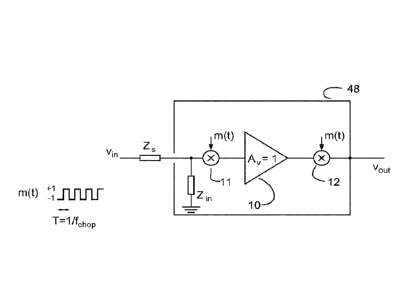
Fig. 1 schematically illustrates an active electrode design according to an
embodiment of
the invention. A bio-potential signal V1(t) is sensed by a capacitive
electrode (not shown)
and fed to an input of an integrated amplifier 10. Impedance, Zs, denotes the
skin-
electrode impedance. On the input of the integrated amplifier 10, the bio-
potential signal
Vin(t) is modulated with a modulation signal (chopper clock), m(t) in a first
mixer 11 in
front of the integrated amplifier 10. The integrated amplifier 10 has a gain
Av equal to
one, whereby the integrated amplifier 10 acts as a buffer, and by applying the
same
chopper modulation signal, m(t), in a second mixer 12 on the output of the
integrated
amplifier 10, too, the integrated amplifier 10 and the two mixers 11 and 12
provide a
buffered path outputting an output signal Vout(t).
The modulation signal m(t) employed in the embodiment shown in fig. 1 is
illustrated as a
pulse-width modulated signal having a duty-cycle of 50%, and assumes a unity
amplitude
of +1 and -1. The chopper frequency, fchop, is selected to ensure that flicker
noise in the
low frequency range will be substantially eliminated. Impedance, Z111, denotes
the finite
input impedance. The choppered buffer output V0(t) is used for driving the
active shield
placed near said electrode and being electric insulated from said electrode.
With reference to fig. 2, the noise spectrum composed by white and pink noise
for a
semiconductor based amplifier is illustrated. The comer frequency fc
characterizes the
border between the region dominated by the low-frequency flicker noise (pink
noise) and
thermal noise which is dominating as the higher frequency "flat-band" noise
(white
noise). Flicker noise occurs in most electronic devices, and provides a
limitation on the
CA 02970757 2017-06-13
WO 2016/096030
PCT/EP2014/078651
7
signal level a circuit may handle. This is illustrated in fig. 2 where
logio(f) is depicted on
the x-axis, and the voltage squared is depicted on the y-axis.
In the current embodiment, the integrated amplifier is realized in a MOSFET
transistor
layout, and a corner frequency in the level of approximately 200 Hz has been
observed.
The comer frequency, tomer, is the transition between the regions dominated by
the low-
frequency flicker noise and the higher frequency "flat-band" noise,
respectively. Therefor
the chopper frequency, fehop, has to be chosen so well above the corner
frequency, so the
frequency shift introduced prior to the integrated amplifier is sufficient to
escape the
flicker noise region of the integrated amplifier. The modulation frequency
providing the
frequency shift is greater than the corner frequency, and according to the
illustrated
embodiment the chopper frequency fchop has been chosen to be in the range from
200 Hz
to 2 kHz. Preferably, chopper frequency fehop is in the range from 400 Hz to 1
kHz. When
the chopper frequency Got, is higher, the power consumption will be adversely
affected.
For an ear-EEG application the sense electrode will pick up a bio-potential
signal Vin(t)
having amplitude at approximately 1iV. The bio-potential signal Vin(t) will in
a first use
situation have a spectral distribution in a basic frequency range between 0
and 35Hz ¨
which is schematically illustrated in fig. 6a. Once modulated with the chopper
signal m(t)
in the mixer 11, the bio-potential signal Vin(t) will be shifted in frequency
so it appears
around the chopper frequency at e.g. 1 kHz as is illustrated in fig. 6b. The
integrated
amplifier will introduce flicker noise in the spectrum up to the corner
frequency e.g. at
200 Hz, while the frequency range above the corner frequency ¨ including the
frequency
shifted bio-potential signal - will only be affected by white, thermal noise.
This is
illustrated in fig. 6c.
In the mixer 12, the output from the integrated amplifier 10 is modulated with
the chopper
signal m(t), where the bio-potential signal is brought back to the basic
frequency range
again, while the flicker noise of the amplifier is positioned around the
chopper frequency.
This is illustrated in fig. 6d. An appropriate low-pass filtering at a later
signal processing
stage will remove the flicker originated noise now present in the frequency
range around
the chopper frequency.
CA 02970757 2017-06-13
WO 2016/096030
PCT/EP2014/078651
8
An active electrode design according to the invention may be designed with low
input-
referred noise, high input impedance and low bias current, low input referred
offset, low
output impedance, high CMRR and PSRR, and low-power consumption. The actual
implementation of an active electrode may be optimized for different
applications, for
example implantable neural probe array and fabric-based use (dry-contact
electrode).
Fig. 3 shows schematically a bio-potential monitoring system employing an
active
electrode design according to an embodiment of the invention. A plurality of
electrodes is
arranged in mesh 30 positioned on the scalp 35 of a user. In another
embodiment, the
electrodes may be provided on an earplug and data may be collected from the
ear canal
and processed in a battery driven data processor placed behind the ear.
Electrodes 31 and
32 do each include a probe 34 being a capacitive sense electrode and an active
shield
electrode placed near but spaced apart from the capacitive sense electrode.
The input
signal picked up by the probes 34 is led to respective amplifiers 10,
preferably arranged
as a unity gain amplifier. The closed-loop unit-gain amplifiers 10 are
connected between
the sense electrode and the active shield electrode. With this arrangement,
the parasitic
capacitor of the sense electrode is effectively reduced, thereby increasing
sensitivity.
The output from the closed-loop unit-gain amplifier 10 with chopper modulation
is via a
shielded cable 13, e.g. a coax cable, fed to a Variable-Gain Amplifier 14
varying the gain
based on a control voltage, and further to an Analog-to-Digital Converter 15
converting
the amplified VB,õ signal into a digital representation for further
processing. The Variable-
Gain Amplifier 14 is a differential amplifier. Shielding is preferred but not
crucial/necessary between the front-end integrated circuit containing the
closed-loop unit-
gain amplifier 10, and the back-end integrated circuit containing the Variable-
Gain
Amplifier 14 and the Analog-to-Digital Converter 15.
In the following there is provided a technical description of the active
electrode using a
choppered buffer according to the invention. Fig 4 illustrates that there
exist several major
parasitic-capacitance contributors in an active electrode concept. A shield 44
is placed
near (and substantially in parallel with) said electrode 43, and the shield 44
is electric
insulated from said electrode 43. There is an electric insulator (not shown)
between the
electrode 43 and the shield 44. This arrangement will cause a capacitive
coupling between
the electrode 43 and the shield 44. The electrode 43 is connected to the
integrated circuit
CA 02970757 2017-06-13
WO 2016/096030
PCT/EP2014/078651
9
via input pads 43a, and a capacitive parasitic coupling there between may be
observed.
The shield 44 is via input pads 48a connected to a shield 48 enclosing the
integrated
circuit, and also here there will be a capacitive parasitic coupling. With
shielding by a
buffer, electrode parasitic capacitances 40 at the sensing electrode and
parasitic
capacitances 41 caused by capacitive couplings between the input pads 48a and
43a can
be compensated.
The active electrode concept shown in fig. 4 illustrates that the amplifier is
implemented
as MOSFET transistors on a substrate (the integrated circuit). The amplifier
is connected
to a power supply 46 and ground 45 via respective contact pads 46a and 45a,
and has an
output terminal 47. The output terminal 47 of the integrated amplifier is
connected to the
shield 48, while the contact pads 45a and 46a are electrical isolated
therefrom. The shield
48 is connected to the output terminal 47 of the integrated amplifier to
actively drive the
electrical potential of the shield 48, thereby providing an active shielding
of the electrode
43. Some capacitances are difficult to compensate, because shielding to their
bottom node
cannot be applied. This count for the parasitic capacitance 42a between the
input pad 49a
and the substrate, the parasitic capacitance between the transistor gate and
the substrate ¨
the gate-to-substrate capacitance 42b, the parasitic capacitance referred
between gate and
source of the transistor ¨ the gate-to-source capacitance 42c, and the
parasitic capacitance
between gate and drain of the transistor ¨ the gate-to-drain capacitance 42d.
In these
circumstances, the objective is to design the circuitry such that the value of
the capacitors
will be as small as possible.
As shown in fig. 5, a choppered buffer according to the invention is
implemented based
on a closed-loop unit-gain amplifier 10 according to the illustrated
embodiment. An input
transistor pair, M1 and M2, of the closed-loop unit-gain amplifier 10 is
minimized in size
in order to reduce the input parasitic capacitances and thereby get high
impedance.
Flicker noise of input transistors M1 and M, is a non-dominant noise source
due to the
employed chopper modulation.
A constant current is maintained through the input transistor pair, M1 and M2,
through the
use of the current source 50 formed by a transistor MN and a voltage source
Vbattõy. The
voltage source Vbattery may according to one embodiment be a coin-cell battery
of the type
used for hearing aids having nominal supply voltage being approximately 1.2 V.
A bias,
CA 02970757 2017-06-13
WO 2016/096030
PCT/EP2014/078651
Vbp, is applied to the gate of the MOSFET transistor MN controlling the
current from the
voltage source Vbatter, fed to the source of the input transistor pair, M1 and
M2.
By maintaining a constant current through the input transistor pair, M1 and
M2, and
5 applying the negative feedback of the unity gain configuration, the gate-
to-source
capacitance 42c (fig. 4) and gate-to-substrate capacitance 42b (fig. 4) to the
sensor input
are minimized.
The illustrated embodiment for implementing the closed-loop unit-gain
amplifier 10 with
10 chopper modulation according to the invention employs three chopper
switches CHOPi,
CHOP2, and CHOP/. The sizes of chopper switches CHOPi, CHOP2, and CHOP3 are
optimized for speed and noise, and in this topology, the chopper switches
CHOP2 and
CHOP3 are arranged inside of the closed-loop unit-gain amplifier 10. Hereby,
by using
the inherent differential nodes, no extra differential nodes will be required.
Furthermore,
this will not limit the bandwidth of the closed-loop unit-gain amplifier 10
with chopper
modulation.
The input chopper switch CHOPi receives the sensed bio-potential signal VII,
as a first
input signal, and the output signal Vein from the closed-loop unit-gain
amplifier 10 via a
feedback branch 53 as a second input signal. The chopper switch CHOPi operates
at 1
kHz chopper frequency. The chopper signal alternates between +1 and -1 at 50%
duty
cycle. The bio-potential signal Vin has a low bandwidth (normally between 0-40
Hz), but
the chopper frequency shall be above the corner, f
-corner (fig. 2). Choosing the chopper
frequency to be too high, will adversely affect the power consumption of the
overall
electrode assembly.
The gates of the input transistor pair, Mi and M2, receive respective outputs
from the
input chopper switch, CHOPi, The constant current from the current source is
passed
through the input transistor pair, M1 and M2 via respective source terminals,
and the
drains of the input transistor pair, M1 and M2, are connected to respective
terminals on the
second chopper switch, CHOP/.
The two outputs from the chopper switch, CHOP2, are connected to respective
source
terminals of a MOSFET transistor pair, M3 and M4. The transistor pair, M3 and
M4, forms
CA 02970757 2017-06-13
WO 2016/096030
PCT/EP2014/078651
11
a source follower (common-drain amplifier) being a Field Effect Transistor
amplifier
topology, typically used as a voltage buffer.
MOSFET transistors M5, M6, M7 and M8 form a cascoded current mirror circuit,
which
would be recognized by a person skilled in the art as being a standard
component in an
operational amplifier. The cascoded current mirror circuit is a two-stage
amplifier
composed of a transconductance amplifier followed by a current buffer. The
third chopper
switch CHOP3 is arranged in between the two stages of the cascoded current
mirror
circuit. The cascoded current mirror circuit improves input-output isolation
as there is no
direct coupling from the output to input.
Three MOSFET Transistors MNc, M9 and M10 are arranged as an extra source
follower.
The three MOSFET Transistors MNc, Mg and M10 are connected to the voltage
source
Vbattery and operated as a level shifter providing lower dc bias to the
transistors M3 and M4
forming the source follower.
Fig. 7 illustrates one embodiment of the chopper switch CHOPi, CHOP2, CHOP3
used in
the choppered buffer topography shown in fig. 5. The chopper switch has a pair
of input
terminals 80 and a pair of output terminals 81. The chopper switch is shielded
by bulks
.. by means of a shield 82, and includes four transistor switches 84, 85, 86,
and 87 ¨ all
controlled by a clock signal, Clk. For the transistor switches 85 and 87, the
clock signal,
Clk is received via respective inverters 88 and 89, whereby the transistor
switches 84 and
86 closes when the clock signal is high, and the transistor switches 85 and 87
closes when
the clock signal is low. The inverters 88 and 89 are NOT gates implementing
logical
negation. Thereby, the four transistor switches 84, 85, 86, and 87 ensures
that a first
terminal of the pair of input terminals 80 alternately connected to a first
and a second
terminal of the output of the pair of output terminals 81. The second terminal
of the pair
of input terminals 80 alternately connected to the second and the first
terminal of the
output of the pair of output terminals 81.
By connecting the bulks or the shield 82 to the buffer output 90, all the
transistor switches
84, 85, 86, and 87 are shielded to eliminate the body effects and extra
current flow
through the bulk nodes. Therefore the bias current will not significantly
change when
input common-mode voltage varies. In addition, the chopping clock is
bootstrapped to
CA 02970757 2017-06-13
WO 2016/096030
PCT/EP2014/078651
12
keep the overdrive voltage and thereby the "ON" resistance of the transistor
switches 84,
85, 86, and 87 substantially constant. In such a way, the current noise and
the thermal
noise are insensitive to input common-mode voltage. A bootstrap circuitry 83
clock signal
and the output buffer signal via the shield 82 and delivers on the output the
chopper clock
signal, Clk, used to open and close the transistor switches 84, 85, 86, and
87. The
bootstrap circuitry 83 deliberately intends to alter the input impedance.
As illustrated in fig. 10, the noise issues may be separated into two
categories: voltage-
domain noise and current-domain noise. Fig. 10 show the excess noise sources
at the
input of chopper amplifier as shown in fig. 5. A man skilled in the art will
understand that
the problems caused by current noise are highly depending on the value of
source
impedance. Since the skin-electrode impedance is relatively large, and subject
to large
variations, in the dry-contact acquisition analog front-end, both two noises
deserve our
concerns.
Voltage-domain noise
Fig. 10 shows the excess noise sources at the input of chopper amplifier. R,
denotes the
skin-electrode resistance. The main voltage noise contributors 60 include the
input
transistor pair, M1 and M2, and the final transistor pair M7 and M8 in the
cascoded
current mirror circuit, due to the high voltage gain from the these MOSFETs
gates. The
voltage noise may be expressed as a result of the flicker noise and the
thermal noise, and
the offset and flicker noise is theoretically removed from low frequency
signal band, due
to the chopper modulation. The dominant component of the residue noise is
thermal
noise, N7noice, of MOSFETs and may be expressed as follows:
Vnoise \f(1 + gm7/gml)(8kT/gml)BW (1)
where BW denotes the bandwidth of interest, gm, the transconductance of
MOSFETs Mõ
k is Boltzmann's constant, and T is the absolute temperature of the component.
Within the
bandwidth between 0.5-100Hz, the integrated noise is approximately 0.29uVrms
when the
chopper frequency is selected to be 1 kHz and the transconductance of the
dominating
MOSFETs has been optimized in order to minimizing the thermal noise.
CA 02970757 2017-06-13
WO 2016/096030
PCT/EP2014/078651
13
From equation (1) it is seen that the noise voltage VIwise is proportional
with the reciprocal
value of the square root of the transistor transconductance. It has been found
that current
consumption of 8itA and noise of 29nV/VITz as acceptable in terms of power and
noise
budget of the system, which has been indicated in fig. 5 by operating the
closed-loop unit-
gain amplifier 10 through the use of the current source 50 providing 8itA.
Current-domain noise
Bias current 61 gives rise to offset across the source impedance. For bio-
signal sensor
amplifiers, the major sources of bias current include leakage in ESD
protection circuitry,
gate leakage of input MOSFETs and base current of bipolar junction
transistors, chopping
activities as well as PCB leakage. The dominant contributors include leakage
of ESD
protection circuitry and current flow caused by periodic chopping activities.
The leakage of ESD protection circuitry is highly dependent on the ESD
techniques and
circuitry properties. Therefore it exists in all the amplifiers and it's hard
to be completely
avoided. Periodic chopping activities give rise to dynamic current flow
through the
chopper switches and switch-capacitor resistance. By definition, the bias
current is the
average current over a relatively long time at the input node. For the CMOS
chopper
amplifiers, such kind of current could be the dominant bias current source
over the others.
It has been observed that the excess noise normally can be regarded as
negligible in
amplifiers with low-source-impedance, for instance, 101cE2-20k12 of wet
electrodes.
However for high-source-impedance, for instance, several hundred kilo ohm to
several
mega ohm of dry-contact electrode, the imperfections like dc offset and
corresponding
output noise will be regarded as problematic.
By applying appropriate design optimization strategies, all the switches may
advantageously be shielded to eliminate the body effects and extra current
flow through
the bulk nodes. Therefore the bias current will not significantly change when
input
common-mode voltage varies. In addition, the chopping clock is bootstrapped to
keep the
overdrive voltage and thereby the 'on' resistance of the switches
approximately a
constant. In such a way, the current noise and the thermal noise are
insensitive to
variation in the input common-mode voltage.
CA 02970757 2017-06-13
WO 2016/096030
PCT/EP2014/078651
14
By ensuring a well optimization of the choppered buffer according to one
embodiment of
the invention, the bias current is quite low. The chopper switches are
naturally shielded
by the buffer and there exist no significant potential differences between
sources and
drains as well as bulks in the switches. Therefore there is no current path in
the chopper.
The current noise for the choppered buffer according to one embodiment of the
invention
has been observed in the level about 0.3fA/VITz. With a 1Mil resistor
connected, the
excess noise density contribution would be 0.3nW. IN/Tz .
The Common-Mode Rejection Ratio (CMRR) of a differential amplifier is the
rejection
by the device of unwanted input signals common to both input leads, relative
to the
wanted difference signal. A high CMRR is required when a differential signal
must be
amplified in the presence of a disturbing common-mode input. Power Supply
Rejection
Ratio (PSRR) is defined as the ratio of the change in supply voltage in the op-
amp to the
equivalent (differential) output voltage it produces. The output voltage will
depend on the
feedback circuit. Chopper modulation has been found to not only reduce the
noise but
also to contribute to the improvement of the CMRR and the PSRR.
The Common-Mode Rejection (CMR) of the amplifier without chopper modulation
has
been observed to be -73.3dB and with chopper modulation the CMR is improved to
-
107.9dB, almost 35dB enhancement in CMRR. Furthermore, the Power Supply
Rejection
(PSR) has been improved with chopper modulation from -48dB to -97.3dB, an
almost
49dB enhancement in PSRR. This has been observed with a capacitance load of
10pF at
the output node for a frequency band (wanted input signal) below 100Hz.
According to the invention there is provided a new choppered buffer employed
in the
active electrode design. Compared with conventional and state-of-art designs,
an active
electrode with choppered buffer exhibits several attractive advantages. Thanks
to the unit-
gain configuration, a well shielding property can be permitted. As a
consequence, ultra-
high input impedance is obtainable, and thereby high CMRR of input impedance
network
could be realized. Chopper modulation shielded by the buffered output
leverages the
voltage-domain and the current-domain accuracies, reaching a good trade-off
compared to
conventional techniques using buffer and chopper amplifier. Besides, a
significant benefit
resulting from chopper modulation is the improved CMRR and PSRR between two
buffer
channels, which could be quite useful to enhance the noise immunity against
surrounding
CA 02970757 2017-06-13
WO 2016/096030
PCT/EP2014/078651
interferences. The subsequent differential amplifier could filter out the
accompanying
chopper spikes and ripples at expense of extra amount of power. The active
electrode with
choppered buffer is very suitable for use in high-quality bio-recording
systems.
5 Fig. 8 shows an embodiment of a sensor system based upon two active
electrodes
according to the invention. The shown sensor system includes a front-end
module 84
being connected to a back-end module 86 via a set of wires 80. The front-end
module 84
includes in the illustrated embodiment a pair active electrodes 43 with
choppered buffer
as described with reference to fig. 1. The choppered buffer is based upon the
integrated
10 amplifier 10 has a gain, Av, equal to one, and two mixers 11 and 12
applying the same
chopper modulation signal, m(t). Furthermore the output terminal 47 of the
choppered
buffer is connected to the shield 48 enclosing the integrated circuit.
Preferably, the active
electrodes operate in differential mode ¨ which means that one of the
electrodes acts as
reference.
The back-end module 86 has a choppered instrumentation amplifier based upon an
integrated amplifier 82 having a gain for amplifying the bio-potential signal
from the
active electrodes, and two mixers 81 and 83 applying the same chopper
modulation
signal, n(t). The chopper modulation signal, n(t) is applied in order to avoid
amplifying
the flicker noise in the integrated amplifier 82.
The chopper clock signal n(t) is preferably a square-wave signal that contains
odd
harmonics at fch, 3fch, 5fch, and as most of the energy of the chopper ripple
is located at
the first harmonics, fch, the higher harmonics may be eliminated by applying a
Chopper
Spike Filter (CSF) 85 providing a low pass or band pass filtering effect. The
Chopper
Spike Filter 85 includes a sample and hold circuit provided by a switch and a
capacitor,
where the switch is driven by sampling pulses. The Chopper Spike Filter 85
removes
glitch caused by the chopper switches. Two branches fed from the output of
choppered
instrumentation amplifier 81-83, but with reverse polarity, has been included
in order to
generate a fully differential output is fed a Programmable Gain Amplifier
(PGA) 87 and
an Analog-to-Digital Converter (ADC) 88, from where the signal is supplied to
a not-
shown microcontroller for processing.
CA 02970757 2017-06-13
WO 2016/096030
PCT/EP2014/078651
16
The choppered instrumentation amplifier 82 may in one embodiment be provided
in
front-end module 84 and thereby included within the active shielding. Then the
number of
thin wires 80 connecting the front-end module 84 to a back-end module 86 may
be
reduced from four to two (shielded) wires. These wires carries supply voltage,
ground,
clock and signal and may in a specific embodiment have a length of 10 mm.
Fig. 9 shows an ear EEG device 115 according to one aspect of the invention.
The ear
EEG device 115 that can be worn inside the ear of a person to be monitored,
e.g. for
detecting Hypoglycemia, e.g. like a per se known In-The-Canal (ITC) hearing
aid.
Furthermore, the device will allow healthcare personal to remote monitor or
record EEGs
for several days at a time. Healthcare personal would then be allowed to
monitor patients
who have regularly recurring problems like seizures or micro-sleep. The ear
EEG device
115 will not interfere with normal life, because the ear EEG device 115 has an
acoustic
vent 116 so the wearer will be able to hear. After a while, the wearer forgets
that he wears
the ear EEG device 115. The ear EEG device 115 is on its outer surface
provided with
two active electrodes 117 according to the invention. Internally the ear EEG
device 115
contains an electronic module 118.
The ear EEG device 115 is formed to fit into the external auditory canal 111
of the
wearer, and defines a cavity in the external auditory canal 111 together with
the tympanic
membrane 110, and the cavity is opened by means of the acoustic vent 116
extending
through the entire length of the ear EEG device 115. Preferably the ear EEG
device 115
does not extend beyond the pinna 112.
The electronic module 118 is shown schematically in enlarged view in the
dotted box
118. The electronic module 118 includes a power supply 120 based upon a
standard
hearing aid battery for powering the electronics. The two electrodes 117
provided on the
surface of the ear EEG device 115 pick up a potential and delivers the data
via a module
125 operating as electrode frontend and Analog to Digital Converter (ADC) to a
digital
signal processor 124. Details of the electrode frontend and ADC module 125 has
been
explained with reference to fig. 8. The digital signal processor 124 receives
the amplified
and digitized signal for processing. According to one embodiment, the digital
signal
processor 124 analyses the EEG signal picked up for detecting hypoglycemia by
CA 02970757 2017-06-13
WO 2016/096030
PCT/EP2014/078651
17
monitoring the brain wave frequency, and if the brain wave frequency falls
beyond a
predefined interval, this may indicate that a medical emergency may arise.
Hypoglycemia
is a medical emergency that involves an abnormally diminished content of
glucose in the
blood. Upon detection of abnormal brain wave activities, the digital signal
processor 124
communicates these findings to a device operating controller 122.
The device operating controller 122 is responsible for several operations and
has an audio
front-end module 123 including a microphone and a speaker. With the
microphone, the
device operating controller 122 is able to pick up audio samples and classify
the current
sound environment. Furthermore, the device operating controller 122 may have
access to
real time clock information ¨ either from an internal clock module or from a
personal
communication device (e.g. a smartphone) accessible via a radio module 121.
The
personal communication device and the radio module 121 may establish a
wireless
communication link by means of a short range communication standard, such as
the
BluetoothTM Low Energy standard. The device operating controller 122 adjusts
the
predefined interval for normal the brain wave activity in dependence to the
real time
clock information and the sound environment classification. With the speaker,
the device
operating controller 122 is able to alert the wearer of the ear EEG device 115
that medical
emergency may arise and that precautionary actions have to be taken.
The number of electrodes has so far been identified as a pair of active
electrodes
operating in differential mode. However two or more active electrodes may be
acting as
sensing electrodes for measuring the electric potential difference relative to
an active
electrode acting as a common reference electrode. The electrodes will operate
in a
unipolar lead mode.
The ear EEG device 1 1 5 may in a further embodiment operate as a hearing aid
if the
processor is provided with a gain for alleviating a hearing loss of the
wearer. The ear EEG
device 115 may advantageously be integrated into an In-The-Canal (ITC) hearing
aid, a
Receiver-In-Canal (RIC) hearing aid or another type of hearing aid.