Note: Descriptions are shown in the official language in which they were submitted.
CA 02971119 2017-06-15
WO 2015/140696
PCT/1B2015/051916
CAPACITOR STRINGS AND APPLICATION THEREOF TO PRECISION
ANALOG PERFORMANCE WITHOUT PRECISION PARTS
FIELD OF THE INVENTION
This invention relates to capacitor strings (or stacks) and the application
thereof to precision
analog performance without precision parts.
BACKGROUND
Nearly all digital integrated circuits require a little bit of analog
circuitry to interface with the
systems they are in. Since these systems do their work in the digital domain,
conversion, or
translation from analog to digital should be done as early as possible and
allow Digital Signal
Processing algorithms do the bulk of the work. Future performance demands on
Digital Signal
Processing will require that a digital signal processor (or "DSP") no longer
calculate, but rather
approximate its results. However, when the speed of processing exceeds what a
DSP can handle,
the only alternative is to pre-process with analog circuits. With the
continual shrink of feature size
on chips, conventional analog approaches are extremely problematic to the
point of failing. A new
paradigm is required: "Analog-in-Digital" (or "AiD") is such a paradigm that
paves the way for the
future. When an engineer can no longer perform analog circuit design, the
engineer is not able to
continue shrinking intact systems.
Digital complementary metal-oxide-semiconductor (or "CMOS") integrated
circuits offer
certain components that have excellent analog properties:
1) Digital metal-oxide semiconductor (or "MOS") transistors possess virtually
zero input
current and have an unusually small input capacitance.
1
CA 02971119 2017-06-15
WO 2015/140696
PCT/1B2015/051916
2) Small, nearly ideal, Metal-Insulator-Metal (or "MIM") capacitors (often
termed cordwood
or fringe capacitors) are made with interconnect traces and the same
insulating material
that separates those traces. The capacitance value of MIMs does not vary with
applied
voltage, and leakage is essentially undetectable, also their equivalent series
resistance (or
"ESR") is exceptionally low. The capacitance values that are available happen
to be
appropriately sized for the requirements of the accompanying devices they are
used with.
MIMs are ideal as "Flying" (floating) capacitors, since they are not
referenced to the
substrate, the power supplies, or any other component in the integrated
circuit.
3) The ON resistance of minimum size Transmission-Gate switches (Pass Gate
logic), is not a
problem because of the very minimal currents flowing in the analog path. The
charge-
injection error of these switches is minimized by the complementary gate drive
signals used
to operate them.
4) The small size components used in AiD circuits allow them to match the
speed of the digital
circuits they are interfaced to. Precision analog is now able to operate at
digital speeds.
In modern integrated circuits there are three common choices when specifying
capacitors.
One uses a reverse biased semiconductor junction, another uses the capacitance
between a metal-
oxide-semiconductor field-effect transistor (or "MOSFET") channel and its gate
lead and the last uses
an insulating oxide to separate two metalized areas. The junction type
capacitor (1st) varies the
thickness of the dielectric (depletion region) as the voltage stored on the
capacitor changes. The
MOSFET capacitor (2nd) also changes its capacitance value as the voltage
stored on the capacitor
changes. But the Metal-Insulator-Metal (MIM) capacitor (3rd) does not change
its capacitance as the
voltage impressed on it changes, because the metal plates and the silicon-
dioxide dielectric are not
influenced by the voltage stored on them. For any given charge on a capacitor,
if the capacitance
changes so does the terminal voltage; so it is imperative for these precision
circuits to use a device
with a stable capacitance value.
2
CA 02971119 2017-06-15
WO 2015/140696
PCT/1B2015/051916
If this same capacitor is connected in a circuit where current is allowed to
flow, the charge
on the capacitor is disturbed. If instead the charge on the capacitor is
merely allowed to create a
field in the gate region of a MOSFET, no current flows in the capacitor but
the conductivity of the
MOSFET channel is affected by the gate charge imposed by the capacitor. This
sensing by high
impedance is a key to the present invention herein described. The stored
analog value remains
undisturbed.
Other high impedance circuit configurations could be used to prevent the
disturbance of the
charge but none perform as well as a simple, unadulterated MOSFET gate. A
differential pair of
MOSFETS in a conventional operational amplifier (or "OP-Amp") configuration
will perform in a
similar fashion but with reduced bandwidth and the OP-Amp cannot operate at
all with the low
power supply voltages available in deep sub-micron environments. Vacuum tubes
might work as
well but a short history lesson will remind us why that choice is not a good
one.
Specifically, precision voltage reference without precision parts is not
possible using a
conventional analog design approach. For example, matched resistors are
commonly used in a
series connection, to provide a sequence of (analog) voltage reference output
taps. This approach is
costly and not even available in the integrated circuit processes where the
feature size is too small to
make matched resistors or even matched capacitors. A series (or stack) of
capacitors, connected
across a voltage reference, will offer multiple voltage outputs at regular
intervals with the same
precision in voltage as is the precision in capacitance. A five percent
deviation in capacitance will
cause a corresponding five percent error in the division of the voltage. The
less than obvious
solution will become obvious in the next section.
SUM MARY
This invention is operable in two phases, "Sample" and "Calculate (or
Reference)" During
the sample phase, input voltage is stored as charge, and in the calculate
phase, the charges are re-
arranged to perform the desired mathematical operation; while the output is
expressed with a
3
CA 02971119 2017-06-15
WO 2015/140696
PCT/1B2015/051916
mechanism that supplies the calculated voltage at necessary current without
consuming charge.
This cycle is repeated at the sample rate, so analog signals are processed at
the rate required by the
associated systems.
According to a preferred embodiment, the present invention provides an
approach to analog
chip design which is accomplished using integrated circuit processes, intended
for digital logic,
available in any digital fab. An analog value, stored as a charge on a high
quality (stable) capacitor, is
measured by a circuit that does not allow current flow out of that capacitor,
thus preserving the
analog value. Furthermore, multiple capacitors can be switched in parallel or
series, as required, to
perform a multitude of desirable functions.
In order to achieve precision without precision parts, a series stack of
capacitors is charged,
then electrically disconnected, and reconfigured to a parallel bank of
capacitors. This allows the
larger capacitors to equalize their terminal voltage with the lesser
capacitors until all the capacitors
are of equal voltage. When reconfigured to a series connection, all of the
capacitors generate equal
amplitude steps, regardless of their capacitive tolerance or matching. The
same equalization process
works in reverse, i.e. capacitors charged in parallel and then reconfigured to
series. Thus the
present invention provides the not so obvious answer to "analog precision
without matched or
precision parts". The alternating series and parallel configuration allows use
of non-precision parts
as found in volume production of integrated circuits while still providing
acceptable levels of
precision.
Stacked capacitors provide the necessary voltage reference sources required
when building
analog to digital converters (or "ADC") and digital to analog converters (or
"DAC"). Finding a
solution to the lack of precision parts has been the "Holy Grail" of the A to
D community from the
beginning. "No precision parts" allows precision analog in an environment that
does not lend itself
to analog precision. The results are totally scalable, stable, low power, all
uncommon to analog
designs. An important additional benefit is that designs are not constrained
to a particular scale or
4
CA 02971119 2017-06-15
WO 2015/140696
PCT/1B2015/051916
vendor's manufacturing process, because the designs are assembled in a digital
integrated circuit
flow using existing digital computer-aided design (or "CAD") tools.
This reparative paradigm eliminates the requirement for precision or precisely
matched
components while generating precision mathematical functions where an analog
solution is required
(such as at high speeds). Small capacitors are used with normal tolerance,
which do not need to be
matched or trimmed when used in circuits with effectively zero current flow.
Process variation and
component degradation with time or environment has negligible effect on
circuit precision where
there is "effectively zero current flow."
BRIEF DESCRIPTION OF THE DRAWINGS:
The invention will now be described in more detail with reference to the
accompanying
drawings, in which:
Fig. 1A is a circuit schematic diagram of 2x amplifier in accordance with the
present
invention;
Fig. 1B is a circuit schematic diagram of 4x amplifier in accordance with the
present
invention;
Fig. 1C is a diagram of Non-Inverting and Inverting Analog Buffers in
accordance with the
present invention;
Fig. 1D is a diagram of Analog Sum and Difference in accordance with the
present invention;
Fig. 1E is a diagram of Integer Multiplication in accordance with the present
invention;
Fig. 1F is a diagram of Integer Division in accordance with the present
invention;
Fig. 1G is a diagram of Analog Averaging in accordance with the present
invention;
5
CA 02971119 2017-06-15
WO 2015/140696
PCT/1B2015/051916
Fig. 2A is a schematic diagram of a simple precision voltage divider in
accordance with the
present invention;
Fig. 2B is a schematic diagram of a simple precision voltage dividing charge
pump in
accordance with the present invention;
Fig. 2C is a schematic diagram of an eight level voltage divider in accordance
with the
present invention;
Fig. 2D is a block diagram, including a 'A step division, in a voltage ladder
of type shown in
Fig. 2C;
Fig. 2E is a detail of a 'A step divider for a voltage ladder of type shown
in Fig. 2D;
Fig. 3A is an improved accuracy three-stage "divider tree" in accordance with
the present
invention;
Fig. 3B is the initial stage voltage waveform plot of a 64 level three-stage
"divider tree" in
accordance with the present invention;
Fig. 3C is the intermediate stage voltage waveform plot of a 64 level three-
stage "divider
tree" in accordance with the present invention;
Fig. 3D is the final stage voltage waveform plot of a 64 level three-stage
"divider tree" in
accordance with the present invention;
Fig. 4A is a simplified block diagram of a driver circuit as may be used for
the FET switches of
Figs 1A to 1G, 2A to 2E, and 3A to 3D;
Fig. 4B is a complete block diagram of a driver circuit as may be used for the
FET switches of
Figs 1A to 1G, 2A to 2E, and 3A to 3D;
Fig. 4C is a detailed diagram of a portion of a driver circuit, as may be used
for the analog
FET switches of Figs 1A to 1G, 2A to 2E, and 3A to 3D;
6
CA 02971119 2017-06-15
WO 2015/140696
PCT/1B2015/051916
Fig. 5A shows a schematic diagram of traditional complementary FET
Transmission-Gate;
Fig. 5B shows a schematic diagram of an optimized complementary FET switch
including the
coincident switch driver of Fig. 4 with reduced charge injection, as used for
an analog switch;
Fig. 5C shows a schematic diagram of precision complementary FETs, offering
lower charge
injection errors;
Fig. 6A, 6B, 6C show illustrative diagrams of precision (charge injection
cancellation) FET
switches, at various analog signal levels, as may be used in circuits shown in
Figs 1A to 1G, 2A to 2E,
and 3A to 3D; and
Fig. 7 is a schematic diagram of an "adaptive" FET switch gate drive circuit,
facilitating lower
turn-off charge injection.
Fig. 8 is an array of relevant integrated circuit capacitor sizes illustrating
the voltage
produced by a single electron and the number of electrons that produce the
maximum usable IC
voltage; thus defining the theoretical maximum dynamic range.
Note that for clarity in these circuit diagrams, when analog and digital
signals are mixed,
dashed signal lines are used for digital signals and solid lines are used for
analog signals.
DETAILED DESCRIPTION OF ILLUSTRATIVE EMBODIMENTS OF THIS INVENTION:
An inverter has an input threshold voltage where, any increase in input
voltage causes the
output to move toward the negative supply and conversely a decrease in input
voltage causes the
output to move toward the positive supply.
The gain of the inverter determines how sensitive the output is to changes on
the input.
7
CA 02971119 2017-06-15
WO 2015/140696
PCT/1B2015/051916
If the output of the inverter is connected directly to the inverter's input,
the voltage on the
output will come to rest at that one unique place where the output voltage is
equal to the inverse of
the input voltage.
If the output, instead of being connected directly to the inverter's input, is
connected in
series with a displacement voltage source and the circuit completed to the
inverter's input, the
output voltage will be displaced by the amount on the displacement voltage
source.
If the inverter input is very high impedance, no current will flow in the
feedback loop,
allowing a capacitor to be used as the displacement voltage source, while not
disturbing the charge
on the capacitor. No current flow means that tolerance variations from
capacitor to capacitor do
not have an effect on the total displacement voltage delivered by multiple
capacitors connected in
series.
The sizes of interconnect metal capacitors available on integrated circuits
are completely
compatible to the accuracies and speed requirements imposed by the inverter
input characteristics
and transmission-gate switch characteristics for near-minimum size CMOS
transistors. Fig. 8 is a
table that illustrates the signal levels incurred and dynamic ranges
available. For instance, a 1pf
capacitor produces 160 nanovolts for each electron it stores. At power supply
voltages this yields a
dynamic range of about 10 million or 7 decades of dynamic range which is
equivalent to 23 bits of
digital resolution. 10pf provides about 8 decades of dynamic range which is
100 million or 27 bits of
digital resolution. The noise floor is determined by a count of electrons not
being where they are
supposed to be.
The output of the inverter can deliver considerable amounts of current while
the feedback
loop maintains the output at the proper displacement voltage.
8
CA 02971119 2017-06-15
WO 2015/140696
PCT/1B2015/051916
Since no current flows in the feedback loop, multiple capacitors can be
connected in series
and/or parallel (with differing polarities - if necessary) to perform a
variety of valuable mathematical
functions.
The inverter can be an op-amp, a digital logic gate or most any gain stage
with inversion
from input to output. While a high input impedance is desirable, a lower input
impedance will work
if the operation is quick enough that displacement voltage droop is
negligible. With a high
impedance input, higher open loop gain allows greater accuracy.
1] 2x amplifier
Fig. 1A illustrates a circuit comprising two capacitors C101 and C102.
In the first
configuration a first set of switches P101, P102 and P103, P104 are closed and
connect the input 101
and 102 to either side of capacitor C101 and capacitor C102 respectively, i.e.
switches P101 and
P102 connects an inverting input voltage 101 to one side of the capacitors
C101 and C102; while
switches P103 and P104 connects a non-inverting input voltage 102 to the other
side of the
capacitors C101 and C102.
In the second configuration capacitors C101 and C102 are arranged in series
with each other
and are further in series with an inverter A101. The circuit in the second
configuration includes a
second set of switches S101, S102, and S103 being closed. Switches S101 and
S102 are arranged to
first and second sides of capacitor C101. Switches S102 and S103 are arranged
to first and second
sides of capacitor C102. At this time the output appears at 103, and is
precisely 2X the voltage that
was presented at the input 101 and 102.
The circuit operates as follows:
1.
Switches P101, P102 and P103, P104 are closed allowing the capacitors C101 and
C102
to charge to the voltage presented at the inverting 101 and non-inverting 102
input
terminals.
9
CA 02971119 2017-06-15
WO 2015/140696
PCT/1B2015/051916
2. Switches P101, P102 and P103, P104 are, then, opened. Then switches
S101, S102, and
S103 are closed connecting the capacitors C101 and C102 in series and placing
the series
string from output 103 of the invertor A101 to input of the invertor A101 as a
displacement voltage. The output at 103 is precisely 2X the voltage that was
presented
at the input 101 and 102. In this configuration, one capacitor offers unity
gain, while
two capacitors offer a gain of two, and "N" number of capacitors would offer a
gain of
,,N
3. It should be noted that there is complete electrical isolation between the
input and
output terminals.
Fig. 1B illustrates a four capacitor arrangement C111, C112, C113, and C114
for a gain of four
(4). As in the description above for Fig. 1A, the circuit of Fig. 1B would be
operated similarly. For
example;
1. A first set of switches, P111, P112, P113, P114, and P115, P116, P117, P118
would be
closed, allowing the capacitors C111, C112, C113, and C114 to be charged to
the voltage
presented at the inverting 111 and non-inverting 112 input terminals.
2. Switches P111, P112, P113, P114, and P115, P116, P117, P118 would then be
opened,
while a second set of switches S111, S112, S113, S114, and S115 are closed to
connect
the capacitors C111, C112, C113, and C114 in series with the invertor A111,
placing the
series string from output 113 of the invertor A111 to input of the invertor
A111, as a
displacement voltage. The output at 113 is precisely 4X the voltage that was
presented
at the input 111 and 112.
Figs. 1C - 1G illustrate several reference examples for analog preprocessing.
The input combinations of the constituent capacitors are shown to the left of
the arrows
along with the description of the arithmetic function. The output
configuration of these same
capacitors is shown to the right of the arrows where the constituent capacitor
combinations create a
CA 02971119 2017-06-15
WO 2015/140696
PCT/1B2015/051916
displacement voltage. The amplifier is represented as an inverter with the
bubble on the input to
indicate that a negative signal on the input produces a positive going signal
on the output.
Fig. 1C illustrates that the polarity of the output 124 or 129 depends solely
on the polarity of
the displacement voltage Va or Va(-) applied, based on inputs 121 or 125 and
to the capacitor Ca.
Fig. 1D further illustrates that more than one input 131 and 132, or 135 and
136 can be
summed by arranging the displacement voltages in series, creating an output
that is the "sum" 134
or the "difference" 139 of the inputs 131 (or Va) and 132 (or Vb), or 135 (or
Va) and 136 (or Vb(-)),
respectively. The difference between the input voltages 135 and 136 is
presented when one of the
displacement voltages (in the feedback loop) is of the opposite polarity.
Fig. 1E illustrates a fixed gain configuration where the gain is equal to the
number of
displacement voltages arranged in series. For example, the input voltage 141
receives two times
(2X) gain at the output 144; while the input voltage 145 receives four times
(4X) gain at the output
149.
In Fig. 1F further illustrates that the input signal Va 151 or 155 is divided
by the number of
capacitors Ca and Cb, or Ca, Cb, Cc and Cd arranged in series on the input,
respectively; and the
parallel arrangement in the feedback loop compensates for any variations in
the values of the
capacitors.
Fig. 1G further illustrates various averaging arrangements, where output 169
is a rough
average of inputs V1 161, V2 162, V3 163, and V4 164; output 179 is rough
weighted average of
inputs V1 171, V2 172, V3 173, and V4 174; and, output 189 is rough
alternating +&- average of
inputs V1 181, V2 182, V3 183, and V4 184. These configurations are referred
to as ROUGH averages
since the input voltages are from different sources. Process variations that
would cause differences
in the capacitors would affect the output voltage.
11
CA 02971119 2017-06-15
WO 2015/140696
PCT/1B2015/051916
Output 179 is a weighted average that is dependent on the weighted value of
its constituent
capacitors Ca, Cb, Cc, and Cd.
Output 189 is applicable as a filter element where the various capacitors
represent the
samples taken at successive 180 degree intervals. The polarity reversals cause
it to operate as a
synchronous demodulator at the same time.
In high speed signal processing, often an approximation is sufficient. In
these situations a
rough average is an approximation, and while there may be an error, the error
will be constant.
Why do rough averaging in hardware when a DSP can perform the function with
precision? The
answer is that averaging in hardware much faster, thus unburdening the DSP.
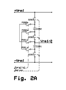
2] Eight output voltage divider
Fig. 2A shows a minimum configuration half-scale voltage ladder. The input
voltages are ¨
Vref and +Vref. The half-scale output voltage is Vref/2. The ladder is
controlled by two logic signals
called "Parallel" and "Series." Initially, the series logic control line
(shorter-dashed interconnect line)
is active to place the two capacitors C201, C202 in series across the
reference voltage inputs ¨Vref to
+Vref. This is connected by series switches S201, S202, and S203.
This is followed by disabling the series connection and then activating the
parallel
connection logic signal (longer dashed line) to connect the two capacitors
C201, C202 in parallel.
This is connected by parallel switches P201a, P202a, and P201b, P202b. During
this parallel
connection time, the capacitor voltages are made precisely equal.
After the parallel connection is disabled, the two capacitors are again placed
in series by
S201, S202, and S203. Since the capacitor voltages were precisely equalized,
the Vref/2 output
voltage is exactly equal to the midpoint between the two reference voltages
¨Vref and +Vref. Due
12
CA 02971119 2017-06-15
WO 2015/140696
PCT/1B2015/051916
to the equalization step, the capacitor tolerances have no effect on the
precision on the voltage
division, thus precision without precision parts or process parameter drift.
Since the ladder structure of Fig 2A is switched the arrangement of capacitors
C211 and
C212 between in series by the series switches S211, S212, S213 and parallel by
parallel switches
P211a, P211b, P212a, P212b, Vref/2 is not constant. In order to provide a
constant output, a
transfer switch T211 is added as shown in Fig. 2B to sub-sample the output
voltage on an output
capacitor C200. The logic line (dot-dashed line) named "Transfer" controls the
transfer switch time,
which is within the series connection time.
Fig. 2C shows a precision voltage reference generator that does not require
any precision or
matched parts. In similar fashion to Fig. 1A, when the series switches S221,
S222, S223, S224, S225,
S226, S227, S228, and S229 are closed, the voltage from the +Vref to -Vref
terminals is divided
across the capacitors C221, C222, C223, C224, C225, C226, C227, and C228 in
proportion to their
capacitance values. When the serial switches S221, S222, S223, S224, S225,
S226, S227, S228, and
S229 are opened and the parallel switches P221a, P221b, P222a, P222b, P223a,
P223b, P224a,
P224b, P225a, P225b, P226a, P226b, P227a, P227b, P228a, and P228b are closed,
the capacitors
C221, C222, C223, C224, C225, C226, C227, and C228 equalize any difference in
their voltage, such
that the stored voltage is precisely identical on each capacitor. When the
switches are again
operated for series connection, each of transfer switches T221, T222, T223,
T224, T225, T226, T227,
and T228 presents their precise division of the reference voltage, thus
forming a precisely divided
voltage independent of capacitor component tolerance.
Half Step Generator
The circuits of the types shown in Fig. 2C and Fig. 3A can be offset by a 'A
step by including a
'A step generator 242 as follows:
When the series/parallel capacitor stack of Fig. 2C, C221 through C228, is in
the parallel
configuration, the voltage across the parallel buss B & C is equal to one
step. If that parallel buss
13
CA 02971119 2017-06-15
WO 2015/140696
PCT/1B2015/051916
voltage is presented to two other capacitors C231, C232, as shown in Fig. 2E,
connected in series
through switches S231, S232, and S233, each of those two capacitors C231, C232
will have 'A of the
"one step" voltage present on the parallel buss. When the parallel capacitors
of Fig. 2C, C221
through C228, are then connected in series and the two 'A step capacitors of
Fig. 2E, C231 and C232,
are connected in parallel through parallel switches P231a, P231b, P232a, and
P232b, and that
parallel pair in Fig. 2E is placed at the bottom of the series string of Fig.
2C (as shown in Fig. 2D) then
the series voltage references on T221 through T228 are elevated to a point
midway between steps
where an Analog to Digital Conversion decision needs to be made, correcting
for rounding errors as
is well understood in the art.
3] Multiple Stage Voltage Reference Ladder
Fig. 3A illustrates an 8 voltage output three step version of a multiple stage
reference ladder
arrangement comprising an eight capacitor string C321, C322, C323, C324, C325,
C326, C327, and
C328, a four capacitor string C311, C312, C313, and C314, and a two capacitor
string C301, C302
being similarly operative as discussed in connection with Figs. 2C, 2D, and
2E. Each set of two or
more capacitors, alternating between series and parallel connection is used to
provide a set of
equally spaced voltage reference sources. In Fig. 3A the series and parallel
capacitor arrangements
are controlled by two separate logic signals "Parallel" and "Series," which
are not both on at the
same time. There is a third "transfer" logic control signal that is used to
uncouple the stages from
each other during the parallel equalization time.
When each series set C301-C302, C311-C314, and C321-C328 of capacitors is
initially
charged to an applied voltage (+Vref, "2/2," and "4/4" all to -Vref ) across
their series string, the
voltage across each individual capacitor is proportionally different by its
capacitance value
mismatch. When these charged capacitors of each previously series connected
string group C301-
C302, C311-C314, and C321-C328 are converted to parallel connections within
each individual
group, the voltage across the individual capacitors of each group is equalized
to the average group
14
CA 02971119 2017-06-15
WO 2015/140696
PCT/1B2015/051916
voltages, because the capacitors of each group are all tied together in
parallel. Thus all these
capacitor voltages become precisely equal, and when these capacitors are
reconnected back to their
starting series connection, the divided reference voltage taps are a precise
division of the applied
voltage creating a precise voltage divider that is independent of component
tolerance. Alternatively
repeating this series-parallel-series connection sequence guarantees precisely
equally divided
voltages suitable for data converters and other applications. Figure 8
suggests the available dynamic
range and noise floor limits for a given size capacitor size. By using the
staged voltage division of Fig.
3A with "Transfer" switches T301¨T302, T311¨T314 higher tolerance, or lower
capacitor values
may be used.
The larger input voltage (+Vref to -Vref) to be divided is sampled with the
first series
configured capacitor string C301, C302 through series switches S301, S302,
S303 initially. This
establishes a rough voltage division on these capacitors C301, C302 that has
accuracy proportional
to their relative capacitor C301, C302 tolerances. This operation is performed
when the "Series"
logic input is active.
Next, after a non-overlapping logic delay time, the "Parallel" logic signal is
activated to place
these capacitors C301, C302 in parallel by means of switches P301a, P302a on
the bottom of the
capacitors C301, C302 and switches P301b, P302b on the tops of capacitors
C301, C302. Connection
these capacitors C301, C302 in parallel guarantees that their voltages become
exactly equal,
regardless of the relative capacitor tolerances.
After another non-overlapping logic delay time, these capacitors C301, C302
are re-
connected in series in the same manner as they were initially connected in
series through switches
S301, S302, S303, only this time these capacitors C301, C302 already had
exactly equal voltages on
them, thus presenting a half-scale output voltage to a transfer switch T301
and output wire 1/2. The
full scale voltage is also transferred by T302 on output wire 2/2. Multiple
cycles of series then
parallel followed by series connections guarantee an exact half-scale voltage
division. Being careful
CA 02971119 2017-06-15
WO 2015/140696
PCT/1B2015/051916
to not short any capacitor voltages together, the transfer switches present
the precise voltages to
the next or middle stage by means of logic control signal named "Transfer" in
Fig. 3A and identified
by alternating short and long dashed line.
The middle stage in Fig. 3A connects 4 capacitors C311, C312, C313, and C314
in series
through switches S311, S312, S313, and S314 with the same "Series" logic
control signal in a similar
manner as the first stage just described. However, the voltages for the middle
stage series
connection are supported by the similar voltages from the previous first stage
through transfer
switches T301, T302. Since there is a step increase of 2 times the number of
capacitors in the middle
stage, each transfer voltage supports two capacitors C311, C312 and C313, C314
here. The higher
CV2 energy of the first stage capacitors enables the use of proportionally
smaller capacitors in the
middle stage. The parallel switches P311a, P312a, P313a, and P314a on the
bottom of the
capacitors C311, C312, C313, and C314 along with P311b, P312b, P313b, and
P314b are used to
connect the top of these capacitors in parallel with the "Parallel" logic
control signal as in the first
stage.
The third stage in Fig. 3A uses 8 capacitors C321, C322, C323, C324, C325,
C326, C327, and
C328 in series for an additional 2 times the divided voltage resolution. The
series voltages are again
supported by their previous stage through transfer switches T311, T312, T313,
and T314.
The final output ladder voltages are presented to the output 0/8 through 8/8
by transfer
switches T321 through T328 with the same "Transfer" logic control signal for
an 8 output voltage
ladder.
In each stage the parallel configuration is used for equalization of the
capacitor voltages
within each of the three stages. During this parallel configuration the
transfer switches isolate the
three stages. When the capacitor strings are re-connected in series, the
output voltage is exactly
16
CA 02971119 2017-06-15
WO 2015/140696
PCT/1B2015/051916
equal to the desired voltage divisions. The parallel switches are
identified by a prefix to their
identification number, the series switches have an "S" prefix, and the
transfer switches have a "T"
prefix letter. The lower voltage capacitor terminal parallel switches have an
"a" letter appended to
their parallel switch identification number and the higher voltage capacitor
terminal switches have a
"b" letter appended to their parallel switch identification number.
It is desirable to minimize the size of the capacitors. At some point the
effects of
unavoidable surrounding parasitics causes an unacceptable error, thus
establishing a lower limit on
capacitor size. To address this limit, series/parallel capacitor circuits can
be arranged in a tree like
structure where (for example) an output level of 64 capacitors is reinforced
by a prior level of 16
capacitors, which is reinforced by the initial level of 4 capacitors. Figs.
3B, 3C, and 3D are waveforms
of a 64 level 3 stage sequential ladder circuit in operation. Fig. 3B is the
waveforms of the first stage
which is 4 capacitor voltages, Fig. 3C is the middle stage (second stage or
Stage 2) which has 16
capacitor voltages, and Fig. 3D is the third stage (or Stage 3) which has 64
capacitor voltages. The
time scales and voltage scales on these 3 waveform plots are identical. This
illustrative example's
time scale is from 2811is to 295us along the x-axis. The first or left portion
of the waveforms, from
281us to 285u.s, represents the time spent in initially charging the capacitor
strings in series. The
middle portion of the waveforms, 285us to 290u.s, is when the capacitor banks
are in parallel to
equalize their voltages. The third or right portion of the waveforms, 290us to
295us is when the
capacitor banks re-enter their series connections. Here all of the output
voltage steps are precisely
the same for each bank. The accuracy limits are consistent with Fig. 8 in that
accuracies of over 30
bits are achievable, and the ladder configuration enables targeting specific
voltage ranges while not
building unused voltage output ranges. By re-directing the ladder hook-up, the
ranges can be
software controlled.
The lower dotted grey line in each plot indicates the analog zero output
voltage, which is
calibrated to 260 millivolts above ground. The upper dotted grey line in each
plot is 1,280 millivolts
17
CA 02971119 2017-06-15
WO 2015/140696
PCT/1B2015/051916
above the analog zero scale voltage to represent the analog full-scale output
voltage, herein
calibrated to 1,540 millivolts (= 260 + 1,280) above ground. Normally this
range would be biased in
the middle as analog zero and swing +640my (or some other appropriate range)
around the analog
zero bias. This calibration scheme yields 64 steps of 2 millivolt output
voltage levels, proceeded with
16 steps of 8 millivolts, which is fed by the first stage of 4 steps of 32
millivolt levels. Each ascending
(earlier) level makes better use of its capacitors by impressing a higher
voltage on each capacitor
(storing more energy per unit of capacitance [V2]), making it less affected by
the parasitics. Lower
energy capacitors loose some percentage of charge when being moved around from
series to
parallel and back to series again. Higher energy capacitors loose the same
amount of charge but a
lower percentage because they store more energy per unit of capacitance and
therefore are less
affected by parasitics (which remain constant). The tree-like structure shown
in Fig. 3 overcomes
this problem by transferring energy from higher voltage capacitors to lower
voltage series strings of
capacitors when the transfer switches are closed.
4] Control Signal Generation for Precision Analog Switches
When implementing precision analog switches, it is important to have rigorous
control over
the timing of the gate control signals. These gate control signals are
complementary and need to
cross each other at the midpoint between the power supply and ground to
minimize control signal
injection. To accomplish this, appropriately sized logic gates are used to
provide signals that switch
at the same time, which are fed to a final output alignment circuit that uses
an "S-RAM" type flip-
flop to ensure coincidence at the midpoint. This allows proper operation in
the presence of
reasonably expected process variations.
Often when switching between different circuit nodes, it is important that the
nodes are not
connected to each other, as is commonly understood in the art. To accomplish
this, it is necessary to
have a "Break-Before-Make" generator, which is simply a AND gate fed by the
logic signal of interest
and a delayed version of the same signal, as is common in the state of the
art. Two to four inverters
18
CA 02971119 2017-06-15
WO 2015/140696
PCT/1B2015/051916
are normally adequate as the delay element, since these inverters
parametrically track variations in
logic speed. The precision timing of the gate drive signals to a complementary
pair of MOSFET
switches significantly affects the precision of the measurements that can be
made. Care is therefore
taken to equalize the delays in the various digital pathways.
Fig. 4A shows a simplified block diagram of the complementary driver circuit
for a FET
switch. The incoming control signal 412, as illustrated by 422A waveform; is
split into two
complementary paths 412, 413 by inverter 403, then processed through an
equalizer "EQ" block 404
such that complementary, and roughly coincidental, outputs 414, 415 are
created. Roughly
coincidental is to say that the rising and falling outputs cross each other at
a point approximately
midway between the power supplies 424A. These signals are further guaranteed
to cross at the
exact midpoint 426A by a cross-coupled regenerative "FF" latch 406 where
slight differences in
timing from the previous stage (due to process or environmental variations)
are cancelled out by the
differential switching thresholds and the rapid switching rate of the latch
circuit 406. The outputs of
the latch 416, 417 are then buffered 428A, as required, then presented to the
appropriate P-channel
and N-channel gates of the FET switches 409.
Fig. 48 shows two instances of Fig. 4A where a single input signal 440,
depicted by 4228
waveform, controls two FET switches 439, 459 that are complementary in their
operation such that
when one switch is OFF, the other is ON. Specifically, "Break-Before-Make"
circuits 432, 452 are
found in Fig. 48 where the input signal 440 is divided into two paths, the top
path 441 being inverted
by inverter 431 is processed and presented at 442, the bottom path processed
by 452 is presented
at 462. These two signals 442 & 462 are guaranteed to NOT both be ON at the
same time. This
"Dead-Band" is accomplished with special logic blocks that insert a delay in
the turn-on signal while
passing a turn-off signal immediately. The signal is then again divided into
complementary paths
442, 443, 462, 463, where the delay caused by the inverters 433, 453 in the
top paths are equalized
such that both signals 444, 445 are coincident and 464, 465 are coincident.
The signals 444, 445 and
19
CA 02971119 2017-06-15
WO 2015/140696
PCT/1B2015/051916
464, 465 at the output of the equalizers (EQ) 434 & 435, and 454 & 455 are
very closely timed 4248
so that the coincident rising and falling edges cross each other at a point
approximately midway
between the positive and negative digital power supply as best as possible,
given variations in
processing and environment. To further ensure the precision of this timing,
the coincident,
complementary signals are presented to a cross-coupled latch (FF) circuit
(436, 456) where the
regenerative feedback of the block adaptively addresses any timing errors that
might remain 4268.
Finally the signals are buffered at buffers 437, 438, 457, 458 for
distribution 4288 to the MOSFET
switch gates 439 and 459 as required. The buffered outputs 448, 449, 468, 469
can drive a single
analog switch or entire banks of switches. A conventional latch driven with a
single-ended signal
produces complementary outputs, but they are not precisely coincident. Driving
the same latch with
truly differential signals produces coincident as well as complementary
outputs.
Fig. 4C shows a logic diagram of a circuit which produces the coincident
differential logic
drive 486, 487 from a single ended input 482. The single ended input signal
482 is inverted by an
inverter 473 (giving both TRUE and NOT_TRUE signals 482, 483) and the paths
are be appropriately
delayed such that both the TRUE and NOT_TRUE signals 486, 487 occur as close
to coincident as
possible. A weakly cross-coupled latch 476, 477, having both its SET and CLEAR
inputs driven at the
same time will then ensure that both its outputs change at precisely the same
time, such that the
edges cross at mid-supply. While the input timing relationships may vary
slightly with process or
environment, the latch is adaptive and locks in the coincident relationship on
its output.
Neither the delay technique nor the latch technique by themselves is
particularly notable,
but in combination they constitute a powerful way to maintain precision in the
presence of a
multitude of limitations.
The waveform 424C, 426C and circuit diagram 453C through 467C are reproduced
from Fig.
48 for reference correlation of this more detailed logic circuitry.
5] Lower Charge Injection Errors for Precision Analog Switches
CA 02971119 2017-06-15
WO 2015/140696
PCT/1B2015/051916
Fig. 5A shows a circuit diagram of a traditional complementary FET switch, as
used for
analog signals. The switch 510 is a complementary pair of CMOS transistors
511, 512 that connect
or break the analog input/output terminal 500 to/from the other analog
output/input terminal 509.
The signal path is bi-directional in that it will pass analog signals in
either direction when ON and
isolate them when OFF.
The switch is operated by a logic input signal 501 and it's inverted 519
complement 504.
Charge feedthrough errors are introduced during the ON to OFF transition.
Equal channel resistance
is used because this switch may carry significant current.
Fig. 59 shows a circuit diagram of an optimized complementary CMOS switch 530
where first
order cancelation of logic feedthrough errors is made with the use of equal
gate capacitance of MOS
transistors 531 and 532 at the analog midpoint voltage. The driven input side
520 of the analog
switch is not normally affected by charge feedthrough errors while the high
impedance loaded
output side 529 normally is affected by charge feedthrough errors. When the
switch 530 is turned
off by its logic control input 521 second order cancellation of charge
feedthrough errors is made by
using complementary coincident gate 539 drive signals 523 and 524 as detailed
in in the description
of Figs. 4A, 49, and 4C above. Additional cancellation of charge feedthrough
errors can be made by
preventing overdrive on the gate as detailed in the description of Fig. 7
below.
Fig. 5C is an alternative circuit, offering lower "charge injection" errors.
Because of the
capacitive coupling of a MOSFET gate to its channel, changes in the gate
control voltage 543, 544
inject an undesirable charge into the channel. Using both a P-channel and N-
channel device in
parallel, making sure the gate drive 559 signals 543, 544 are complementary in
phase and timing as
detailed in Figs. 4A, 49, and 4C, somewhat improves performance. Even slight
differences in the
gate-to-channel capacitance of P-channel 552 and 554 and N-channel 551 and 553
devices of similar
size (area) operate counter to the objective of charge cancelling. Adding
additional transistors 555,
21
CA 02971119 2017-06-15
WO 2015/140696
PCT/1B2015/051916
556, 557, and 558 configured as capacitors improves the otherwise mismatched
situation, thus
decreasing the signal injection as shown in Figs. 6A, 6B, and 6C below.
6] Precision Charge-Injection Cancellation FET Switch
The charge injection problem comes from two sources. The 1st and most obvious
is
capacitive coupling from the gate drive signal through the gate to channel
capacitance and into the
channel where the signal of interest is traveling. The second and less
obvious, source is the result of
the reduction of the gate to channel capacitance as the channel disappears.
The energy stored in
the gate to channel capacitance will flow towards the path of least resistance
and since the gate
drive is a low impedance source, the charges flow towards the signal of
interest traveling through
the channel.
Figs. 6A, 6B, and 6C are depictions of charge distribution in a transmission-
gate at various
operating voltages. Excess carriers create a problem when the transmission-
gate is switched off.
These excess carriers, in the channel, are literally squeezed out both the
drain and source terminals
of the transmission-gate. Additional transistors guarding the analog input and
output terminals, of
the transmission-gate, provide a reservoir where these excess charges can be
absorbed rather than
appearing as noise injected in the analog path. The amount of charge retained
in the channel varies
with the present analog voltage on the transmission-gate. The guard
transistors have an equal but
opposite charge, thus the charges cancel when the transmission-gate is
switched off. In order to
provide good charge cancellation, all transistors are made to be as identical
to each other as
practical. This includes both the switch transistors and the guard
transistors. For this, the pass
transistors are made up of two series transistors with their series connection
nodes tied together
600x, 610x, 640x, 650x, 670x, and 680x.
In Fig. 6A, top diagram represents when the transmission-gate is switched ON
while bottom
diagram represents when the transmission gate is switched OFF. The operating
voltage presented at
the I/0 terminal is at 90% of Vdd. It can be seen that when the switch is ON
(top), transistors 602
22
CA 02971119 2017-06-15
WO 2015/140696
PCT/1B2015/051916
and 604 are conducting and so have an abundance of carriers in the channel.
When the
transmission-gate is switched OFF (bottom) the guard transistors 616 and 618
absorb the excess
carriers that would have otherwise been injected into the signal path. The
channel charge of the ON
transistors 601, 602, 603, 604 has been transferred to the empty guard
transistors 605, 606, 607,
608 when the switch is turned OFF as shown with switch transistors 611, 612,
613, 614 and the
guard transistors 615, 616, 617, 618.
In Fig. 68 the operating voltage presented at the I/0 terminal is at 50% of
Vdd. It can be
seen that when the switch is ON (top), transistors 641 & 642 and 643 & 644 are
all conducting and
have a similar amount of carriers in their channel. When the transmission-gate
is switched OFF
(bottom) the guard transistors 655 & 656 and 657 & 658 absorb the excess
carriers that would have
otherwise been injected into the signal path. The channel charge of the ON
transistors 641, 642,
643, 644 has been transferred to the empty guard transistors 645, 646, 647,
648 when the switch is
turned OFF as shown with switch transistors 651, 652, 653, 654 and the guard
transistors 655, 656,
657, 658.
In Fig. 6C the operating voltage presented at the I/0 terminal is at 10% of
Vdd. It can be
seen that when the switch is ON (top), transistors 661 and 663 are conducting
and so have an
abundance of carriers in the channel. When the transmission-gate is switched
OFF (bottom) the
guard transistors 675 and 677 absorb the excess carriers that would have
otherwise been injected
into the signal path. The channel charge of the ON transistors 661, 662, 663,
664 has been
transferred to the empty guard transistors 665, 666, 667, 668 when the switch
is turned OFF as
shown with switch transistors 671, 672, 673, 674 and the guard transistors
675, 676, 677, 678.
In order to cancel the undesired interference from the drive signals, it is
imperative that the
guard and transmission transistors be as identical as possible. It should be
noted that the guard
transistors have their source and drain terminals shorted so that they cannot
impede the analog
signal of interest. It should further be noted that the gate drive signals
presented to the guard
23
CA 02971119 2017-06-15
WO 2015/140696
PCT/1B2015/051916
transistors are of the inverse phase as those presented to their neighboring
transmission-gate
transistor. In Fig. 6A the channel charge of the ON transistors 601, 602, 603,
604 has been
transferred to the empty guard transistors 605, 606, 607, 608 when the switch
is turned OFF as
shown with switch transistors 611, 612, 613, 614 and the guard transistors
615, 616, 617, 618.
7] Alternative "Adaptive" Gate Drive Circuit to lower charge injection errors
Fig. 7 shows a circuit diagram of an alternative adaptive gate drive circuit
to lower charge
injection error. Its analog input is 770 which is amplified by amplifier 771
to derive a driven amplifier
output 778. Charge injection is reduced at switch turn-off, by limiting the
swing of the transmission-
gate drive signals 774, 775 to the present amplifier 771 output voltage 778,
instead of swinging all
the way to the power supply rails. For this, transistors 776 and 777 are tied
from amplifier output to
their respective switch drivers 776, 775. The low impedance of the amplifier
output makes it
appropriate for this use. The transmission-gate transistors are both turned
off because their gate to
source voltage is clamped 776, 777 to zero with respect to their turn-on
threshold voltage.
DEFINITION OF TERMS
The term "capacitor" herein is intended to encompass charge storage devices in
general.
The term "flying capacitor" refers to a capacitor/switch combination where
both ends of the
capacitor are switched simultaneously and neither end is connected to a fixed
node.
The term "sweet-spot" refers to the input voltage that is discovered when
feedback around
an inverter causes its output voltage to be equal to the inverse of its input
voltage.
The term "i-FET" refers to a new FET structure where besides the standard
source ¨ drain -
gate and body connections, there is a fifth low-impedance connection that
allows a current rather
than a gate voltage to affect the conductivity in the channel between source
and drain.
24
CA 02971119 2017-06-15
WO 2015/140696 PCT/1B2015/051916
The term "precision" refers to the ability to repeat a process or measurement
and achieve
the same resolution of results each time.
The term "logic-only process" is where the possible results are expressed as
true or false.
The term "Analog-in-Digital" refers to a circuit design approach where a
"logic-only process"
is coerced into generating results other than true or false, specifically
analog values.