Note: Descriptions are shown in the official language in which they were submitted.
CA 02971589 2017-06-19
WO 2016/100049
PCMJS2015/064848
Title
Chemically-Sensitive Field Effect Transistor
(EGC-003PCT)
Technical Field
The present invention generally relates to field effect transistors. More
specifically, the present invention relates to one dimensional and two
dimensional
field effect transistors.
Background Art
[0001] The sequencing of Nucleic Acids, such as deoxyribonucleic acid
(DNA), is a fundamental part of biological discovery. Such detection is useful
for a variety of purposes and is often used in scientific research as well as
medical advancement. For instance, the genomics and bioinformatics fields
are concerned with the application of information technology and computer
science to the field of molecular biology. In particular, bioinformatics
techniques can be applied to process and analyze various genomic data, such
as from an individual so as to determine qualitative and quantitative
information about that data that can then be used by various practitioners in
the development of diagnostic, prophylactic, and/or therapeutic methods for
detecting, preventing or at least ameliorating diseased states, and thus,
improving the safety, quality, and effectiveness of health care. The need for
such diagnostic, therapeutic, and prophylactic advancements has led to a high
demand for low-cost sequencing, which in turn has driven the development of
high-throughput sequencing, termed as Next generation sequencing (NGS).
[0002] Generally, the approach to DNA analysis, such as for genetic
diagnostics and/or sequencing, involves nucleic acid hybridization and
detection. For example, various typical hybridization and detection approaches
include the following steps. For genetic analysis, an RNA or DNA sample of a
subject to be analyzed may be isolated and immobilized on a substrate, a
probe of a known genetic sequence, e.g., a disease marker, may be labeled and
washed across the substrate. If the disease marker is present, a binding event
CA 02971589 2017-06-19
WO 2016/100049
PCMJS2015/064848
2
will occur, e.g., hybridization, and because the probe has been labeled the
hybridization event may either be or not be detected thereby indicating the
presence or absence of the disease marker in the subject's sample.
[0003] For DNA sequencing, first, an unknown nucleic acid sequence to
be
identified, e.g., a single-stranded sequence of DNA of a subject, is isolated,
amplified, and immobilized on a substrate. Next, a known nucleic acid labeled
with an identifiable tag is contacted with the unknown nucleic acid sequence
in the presence of a polymerase. When hybridization occurs, the labeled
nucleic acid binds to its complementary base in the unknown sequence
immobilized on the surface of the substrate. The binding event can then be
detected, e.g., optically or electircally. These steps are then repeated until
the
entire DNA sample has been completely sequenced. Typically, these steps are
performed by a Next Gen Sequencer wherein thousands to millions of
sequences may concurrently be produced in the next-generation sequencing
process.
[0004] For example, a central challenge in DNA sequencing is
assembling
full-length genomic sequences, e.g., chromosomal sequences, from a sample
of genetic material and/or mapping and aligning sample sequence fragments to
a reference genome, yielding sequence data in a format that can be compared
to a reference genomic sequence such as to detet mine the variants in the
sampled full-length genomic sequences. In particular, the methods employed
in sequencing protocols do not produce full-length chromosomal sequences of
the sample DNA.
[0005] Rather, sequence fragments, typically from 100-1,000
nucleotides in
length, are produced without any indication as to where in the genome they
align. Therefore, in order to generate full length chromosomal genomic
constructs, or determine variants with respect to a reference genomic
sequence, these fragments of DNA sequences need to be mapped, aligned,
merged, and/or compared to a reference genomic sequence. Through such
CA 02971589 2017-06-19
WO 2016/100049
PCT/US2015/064848
3
processes the variants of the sample genomic sequences from the reference
genomic sequences may be determined.
[0006] However, as the human genome is comprised of approximately 3.1
billion base pairs, and as each sequence fragment is typically only from 100
to
500 to 1,000 nucleotides in length, the time and effort that goes into
building
such full length genomic sequences and determining the variants therein is
quite extensive often requiring the use of several different computer
resources
applying several different algorithms over prolonged periods of time.
[0007] In a particular instance, thousands to millions of fragments or
even
billions of DNA sequences are generated, aligned, and merged in order to
construct a genomic sequence that approximates a chromosome in length. A
step in this process may include comparing the DNA fragments to a reference
sequence to determine where in the genome the fragments align.
[0008] The genetic material must be pre-processed, so as to derive
usable
genetic sequence data. This preprocessing may be done manually or via an
automated sequencer. Typically, preprocessing involves obtaining a biological
sample from a subject, such as through venipuncture, hair, etc. and treating
the
sample to isolate the DNA therefrom. Once isolated the DNA may be
denatured, strand separated, and/or portions of the DNA may then be
multiplied, e.g., via polymerase chain reaction (PCR), so as to build a
library
of replicated strands that are now ready to be read, such as by an automated
sequencer, which sequencer is configured to read the replicate strands, e.g.,
by
synthesis, and thereby determine the nucleotide sequences that makes up the
DNA. Further, in various instances, such as in building the library of
replicated strands, it may be useful to provide for over-coverage when
preprocessing a given portion of the DNA. To perform this over-coverage,
e.g., using PCR, may require increased sample preparation resources and time,
and therefore be more expensive, but it often gives an enhanced probability of
the end result being more accurate.
CA 02971589 2017-06-19
WO 2016/100049
PCT/US2015/064848
4
[0009] Once the library of replicated strands has been generated they
may be
injected into an automated sequencer that may then read the strands, such as
by synthesis, so as to determine the nucleotide sequences thereof. For
instance, the replicated single stranded DNA may be attached to a glass bead
and inserted into a test vessel, e.g., an array. All the necessary components
for
replicating its complementary strand, including labeled nucleotides, are also
added to the vessel but in a sequential fashion. For example, all labeled "A",
"C", "G", and "T's" are added, either one at a time or all together to see
which
of the nucleotides is going to bind at position one. After each addition a
light,
e.g., a laser, is shone on the array. If the composition fluoresces then an
image
is produced indicating which nucleotide bound to the subject location. More
particularly, where the nucleotides are added one at a time, if a binding
event
occurs, then its indicative fluorescence will be observed. If a binding event
does not occur, the test vessel may be washed and the procedure repeated until
the appropriate one of the four nucleotides binds to its complement at the
subject location, and its indicative fluorescence is observed. Where all four
nucleotides are added at the same time, each may be labeled with a different
fluorescent indicator, and the nucleotide that binds to its complement at the
subject position may be determined, such as by the color of its fluorescence.
This greatly accelerates the synthesis process.
[00010] Once a binding event has occurred, the complex is then washed and the
synthesis steps are repeated for position two. For example, a marked
nucleotide "A" may be added to the mix to determine if the complement at the
position is a "T", and if so, all the sequences having that complement will
bind
to the labeled "T" and will therefore fluoresce, and the samples will all be
washed. Where the binding happened the bound nucleotide is not washed
away, and then this will be repeated for all nucleotides for all positions
until
all the over-sampled nucleic acid segments, e.g., reads, have been sequenced
and the data collected. Alternatively, where all four nucleotides are added at
the same time, each labeled with a different fluorescent indicator, only one
CA 02971589 2017-06-19
WO 2016/100049
PCT/US2015/064848
nucleotide will bind to its complement at the subject position, and the others
will be washed away, such that after the vessel has been washed, a laser may
be shone on the vessel and which nucleotide bound to its complement may be
determined, such as by the color of its fluorescence.
5 [00011] This continues until the entire strand has been replicated in
the vessel.
Usually a typical length of a sequence replicated in this manner is from about
100 to about 500 base pairs, such as between 150 to about 400 base pairs,
including from about 200 to about 350 base pairs, such as about 250 base pairs
to about 300 base pairs dependent on the sequencing protocol being employed.
Further, the length of these segments may be predetermined, e.g., engineered,
to accord with any particular sequencing machinery and/or protocol by which
it is run. The end result is a readout, or read, that is comprised of a
replicated
DNA segment, e.g., from about 100 to about 1,000 nucleotides in length, that
has been labeled in such a manner that every nucleotide in the sequence, e.g.,
read, is known because of its label. Hence, since the human genome is
comprised of about 3.2 billion base pairs, and various known sequencing
protocols usually result in labeled replicated sequences, e.g., reads, from
about
100 or 101 bases to about 250 or about 300 or about 400 bases, the total
amount of segments that need to be sequenced, and consequently the total
number of reads generated, can be anywhere from about 10,000,000 to about
40,000,000, such as about 15,000,000 to about 30,000,000, dependent on how
long the label replicated sequences are. Therefore, the sequencer may
typically
generate about 30,000,000 reads, such as where the read length is 100
nucleotides in length, so as to cover the genome once.
[00012] However, in part, due to the need for the use of optically detectable,
e.g., fluorescent, labels in the sequencing reactions being performed, the
required instrumentation for performing such high throughput sequencing is
bulky, costly, and not portable. For this reason, a number of new approaches
for direct, label-free detection of DNA sequencing have been proposed. For
instance, among the new approaches are detection methods that are based on
CA 02971589 2017-06-19
WO 2016/100049
PCT/US2015/064848
6
the use of various electronic analytic devices. Such direct electronic
detection
methods have several advantages over the typical NGS platform. For example,
the detector may be incorporated in the substrate itself, such as employing a
biosystem-on-a-chip device, such as a complementary metal oxide
semiconductor device, "CMOS". More particularly, in using a CMOS device
in genetic detection, the output signal representative of a hybridization
event
can be directly acquired and processed on a microchip. In such an instance,
automatic recognition is achievable in real time and at a lower cost than is
currently achievable using NGS processing. Moreover, standard CMOS
devices may be employed for such electronic detection making the process
simple, inexpensive, and portable.
[00013] Particularly, in order for next-generation sequencing to become widely
used as a diagnostic in the healthcare industry, sequencing instrumentation
will need to be mass produced with a high degree of quality and economy.
One way to achieve this is to recast DNA sequencing in a format that fully
leverages the manufacturing base created for computer chips, such as
complementary metal-oxide semiconductor (CMOS) chip fabrication, which is
the current pinnacle of large scale, high quality, low-cost manufacturing of
high technology. To achieve this, ideally the entire sensory apparatus of the
sequencer could be embodied in a standard semiconductor chip, manufactured
in the same fab facilities used for logic and memory chips. Recently, such a
sequencing chip, and the associated sequencing platform, has been developed
and commercialized by Ion Torrent, a division of Thermo-Fisher, Inc. The
promise of this idea has not been realized commercially due to the
fundamental limits of applying a metal oxide semiconductor field effect
transistor, or MOSFET, as a bio sensor. When a MOSFET is used in solution
as a biosensor, it is referred to as an ISFET. A particular limitation
includes a
lack of sensor sensitivity and signal to noise characteristics as the
semiconductor node scales down to lower geometries of the transistor (gate
length).
CA 02971589 2017-06-19
WO 2016/100049
PCT/US2015/064848
7
[00014] More particularly, a field effect transistor, FET, typically
includes a
gate, a channel region connecting source and drain electrodes, and an
insulating barrier separating the gate from the channel. The operation of a
conventional FET relies on the control of the channel conductivity, and thus
the drain current, by a voltage, VGS, applied between the gate and source. For
high-speed applications, and for the purposes of increasing sensor
sensitivity,
FETs should respond quickly to variations in VGS. However, this requires
short gates and fast carriers in the channel. Unfortunately, FETs with short
gates frequently suffer from degraded electrostatics and other problems
(collectively known as short channel effects), such as threshold-voltage roll-
off, drain-induced barrier lowering, and impaired drain-current saturation,
which results in a decrease in sensor sensitivity. Nevertheless, scaling
theory
predicts that a FET with a thin barrier and a thin gate-controlled region
(measured in the vertical direction) will be robust against short-channel
effects
down to very short gate lengths (measured in the horizontal direction).
[00015] Accordingly, the possibility of having channels that are very thin in
the
vertical dimension would allow for high-speed transmission of carriers as well
as for increased sensor sensitivity and accuracy. What is needed, therefore,
is a
FET device that is configured in such a manner as to include a shorter gate
than is currently achievable in present FET applications. A solution that
includes such a FET device designed for use in biological applications, such
as
for nucleic acid sequencing and/or genetic diagnostics would especially be
beneficial.
Summary of the Invention
[00016] The present invention is a chemically-sensitive field-effect
transistor
that solves many of the current problems associated with nucleic acid
sequencing and genetic diagnostics.
[00017] One aspect of the present invention is a chemically-sensitive
field
effect transistor. The chemically-sensitive field effect transistor comprises
an
CA 02971589 2017-06-19
WO 2016/100049
PCT/US2015/064848
8
integrated circuit structure comprising a conductive source and a conductive
drain and a channel. The channel extends from the conductive source to the
conductive drain. The channel is composed of a one-dimensional transistor
material or a two-dimensional transistor material. An I-V curve or an I-Vg
curve is shifted in response to a chemical reaction occurring on or near the
chemically-sensitive field effect transistor.
[00018] Another aspect of the present invention is a bio-sensor. The bio-
sensor
includes a semiconductor structure comprising a conductive source and a
conductive drain, a 2D material channel (e.g. a graphene channel) or a 1D
material channel (e.g. a Carbon NanoTube (CNT)) extending from the source
to the drain and a well structure positioned on or over a portion of an
exterior
surface or topmost portion of the channel. The 1D or 2D material comprising
the channel may be covered by a dielectric layer or may have no covering
such that the well structure defines an opening allowing for direct contact
with
the either the dielectric layer or the 1D or 2D material channel. An I-Vg
curve
is shifted in response to detection of a biological compound.
[00019] Yet another aspect of the present invention is a 1D or 2D material
field
effect transistor such as a graphene field effect transistor or GFET. The GFET
includes a structure comprising a conductive source, a conductive drain, and a
graphene channel extending from the source to the drain. An I-Vg curve is
shifted in response to a chemical reaction occurring on the graphene field
effect transistor.
[00020] Yet another aspect of the present invention is a chemically-sensitive
field effect transistor comprising an integrated circuit structure, a channel
and
an oxide layer. The integrated circuit structure comprises a conductive source
and a conductive drain. The channel extends from the conductive source to the
conductive drain. The channel is composed of a one-dimensional transistor
material or a two-dimensional transistor material The oxide layer is disposed
over the channel. The I-V curve or an I-Vg curve is shifted in response to a
84021645
9
chemical reaction occurring on the graphene field effect transistor.
[0020] Yet another aspect of the present invention is a chemically-
sensitive field effect
transistor comprising an integrated circuit structure, a channel and an oxide
layer. The
integrated circuit structure comprises a conductive source and a conductive
drain. The
channel extends from the conductive source to the conductive drain. The
channel is
composed of a one-dimensional transistor material or a two-dimensional
transistor
material. The oxide layer is disposed over the channel. The I-V curve or an I-
Vg curve is
shifted in response to a chemical reaction occurring over or near the
chemically-sensitive
field effect transistor.
[0021] Yet another aspect of the present invention is a bio¨sensor
comprising a
complementary metal-oxide-semiconductor ("CMOS") structure, a graphene
channel, an
oxide layer, and a well structure. The CMOS structure comprises a damascene
copper
source and a damascene copper drain. The graphene channel extends from the
source to
the drain. The oxide layer is disposed over the graphene channel and has a
thickness of 50
nanometers or less. The well structure is positioned over a portion of an
exterior surface of
the oxide layer. The well structure defines an opening allowing for direct
contact with the
oxide layer. An I-V or I-Vg curve is shifted in response to detection of a
biological
compound.
[0022] Yet another aspect of the present invention is a graphene field
effect transistor
comprising a CMOS structure, a graphene channel, an oxide layer, and a well
structure.
The CMOS structure comprises a copper source and a copper drain. The graphene
channel
extends from the source to the drain. The oxide layer is disposed over the
graphene
channel and has a thickness of 50 nanometers or less. The well structure is
positioned over
a portion of an exterior surface of the oxide layer. The well structure
defines an opening
allowing for direct contact with the oxide layer. An I-V or I-Vg curve is
shifted in
response to detection of a biological compound.
[0022a] Yet another aspect of the present invention is a chemically-sensitive
field effect
transistor having a multi-layered structure for performing a sequencing
reaction involving
the sequencing of strands of nucleic acids , the field effect transistor,
comprising: a
substrate layer having an extended body; a first insulating layer positioned
above the
Date Recue/Date Received 2020-11-18
84021645
9a
extended body of the substrate layer; a second insulating layer positioned
above the first
insulating layer; a source electrode and a drain electrode each having a top
surface and a
bottom surface, the top surface separated from the bottom surface by opposing
outer and
inner side portions, each of the opposed side portions and each of the bottom
surfaces of
the source and drain electrodes being disposed within the first insulating
layer, the source
electrode being separated from the drain electrode by a distance; a graphene
layer
positioned between the first insulating layer and second insulating layer and
extending
between the outer side portion of the source electrode and the outer side
portion of the
drain electrode thereby forming a channel between the source electrode and
drain
electrode, the graphene layer contacting the top surface of the source
electrode and drain
electrode; and a reaction chamber formed by a well structure provided in the
second
insulating layer, the well structure having an opening at a top surface of the
second
insulating layer and extending toward the graphene layer the graphene layer
forming a
bottom layer of the reaction chamber, the reaction chamber configured for
receiving and
retaining one or more reactants therein for performing the sequencing
reaction.
[0022b] Yet another aspect of the present invention is a chemically-sensitive
field effect
transistor having a multi-layered structure for performing a biological
reaction involving
one or more of a deoxyribonucleic acid, a ribonucleic nucleic acid, and a
protein , the field
effect transistor comprising: a substrate layer having an extended body; a
first insulating
layer positioned above the extended body of the substrate layer; a source
electrode and a
drain electrode positioned in or over the first insulating layer, the source
electrode
separated from the drain electrode by a distance; a second insulating layer
positioned
above the first insulating layer and proximate the source and drain
electrodes; a graphene
layer positioned between the first and second insulating layers and extending
between the
source and drain electrodes thereby forming a channel between the source
electrode and
drain electrode; and a reaction chamber formed by a well structure provided in
the second
insulating layer, the well structure having an opening at a top surface of the
second
insulating layer and extending toward the graphene layer, the graphene layer
substantially
extending between an outer side portion of the drain electrode and an outer
side portion of
the source electrode and forming a bottom layer within the reaction chamber,
the reaction
Date Recue/Date Received 2020-11-18
84021645
9b
chamber configured for receiving and retaining one or more of a
deoxyribonucleic acid, a
ribonucleic nucleic acid, and a protein therein for performing the biological
reaction.
[0022c] Yet another aspect of the present invention is a chemically-sensitive
field effect
transistor having a multi-layered structure for performing a biological
reaction involving
fluidic reagents within a fluid, the field effect transistor comprising: a
substrate layer
having an extended body; a first insulating layer positioned above the
extended body of
the substrate layer; a source electrode and a drain electrode positioned in or
over the first
insulating layer, the source electrode and the drain electrode being separated
by a distance;
a second insulating layer positioned above the first insulating layer and
proximate the
source and drain electrodes; a graphene layer positioned between the first and
second
insulating layers and substantially extending between an outer side portion of
the drain
electrode and an outer side portion of the source electrode to form a channel
between the
source and drain electrodes; and a reaction chamber formed by a well structure
provided
in the second insulating layer, the well structure having an opening therein,
the opening
defined by opposed side portions and a bottom formed at least by the graphene
layer, the
reaction chamber configured for receiving and retaining one or more of the
reagents in a
fluid therein for performing a biological reaction.
[0022d] Yet another aspect of the present invention is a chemically-sensitive
field effect
transistor having a multi-layered structure for performing a biological
reaction, the field
effect transistor comprising: a substrate layer, the substrate layer having an
extended body;
a first insulating layer positioned above the extended body of the substrate
layer; a source
electrode and a drain electrode positioned in the first insulating layer, the
source electrode
separated from the drain electrode by a distance; a second insulating layer
positioned
above the first insulating layer and proximate the source and drain
electrodes; a graphene
layer positioned between the first and second insulating layers and
substantially extending
between an outer side portion of the source electrode and an outer side
portion of the drain
electrodes to form a channel there-between; and a reaction chamber formed by a
well
structure provided in the second insulating layer, the well structure having
an opening, the
opening including opposing side portions and a bottom formed by at least the
graphene
Date Recue/Date Received 2020-11-18
84021645
9c
layer, the reaction chamber configured for receiving and retaining one or more
reactants
therein for performing the biological reaction.
Brief Description of the Drawings
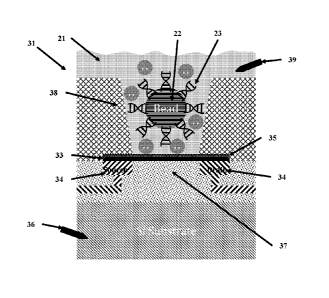
[0023] FIG. 1 is a cross-section diagram of a chemically-sensitive field-
effect transistor
utilized for analysis of biological or chemical materials.
[0024] FIG. lA is a cross-section diagram of a chemically-sensitive field-
effect transistor
utilized for analysis of biological or chemical materials.
[0025] FIG. 2 is a cross-section diagram of a chemically-sensitive field-
effect transistor
with a well structure.
[0026] FIG. 2A is a cross-section diagram of a chemically-sensitive field-
effect transistor
with a well structure.
Date Recue/Date Received 2020-11-18
CA 02971589 2017-06-19
WO 2016/100049
PCT/US2015/064848
[00027] FIG. 3 is a cross-section diagram of a chemically-sensitive field-
effect
transistor.
[00028] FIG. 3A is a cross-section diagram of a chemically-sensitive field-
effect transistor.
5 [00029] FIG. 4 is a top plan view of a chemically-sensitive field-effect
transistor with a well structure.
[00030] FIG. 5 is a block diagram of a system for analysis of biological or
chemical materials.
[00031] FIG. 6 is a top plan view of an array comprising multiple chemically-
10 sensitive field-effect transistors.
[00032] FIG. 7 is an illustration of graphene.
[00033] FIG. 8 is a graph of average sensitivity of a graphene FET ("GFET")
calculated as a function of liquid gate potential.
[00034] FIG. 9 is an illustration of a graphene field-effect
transistor.
[00035] FIG. 10 is a graph of I-Vg curves for various pH values.
[00036] FIG. 11 is a graph of frequency vs. normalized power spectral density
for a silicon ISFET.
[00037] FIG. 12 is a graph of frequency vs. normalized power spectral density
for a typical graphene FET.
[00038] FIG. 13 is a graph of frequency vs. normalized power spectral density
for a graphene FET of the present invention.
[00039] FIG. 14 is a graph of noise vs. bias voltage.
[00040] FIG. 15 is a graph of Dirac voltage vs. current increase.
[00041] FIG. 16 is a graph of current increase vs. pH increase.
[00042] FIG. 17 is an illustration of molybdenum disulfide.
[00043] FIG. 18 is an illustration of black phosphorous.
[00044] FIG. 19 is an illustration of a nanotube
[00045] FIG. 20 is an illustration of silicene.
[00046] FIG. 21 is an illustration of a semiconductor nanowire structure.
CA 02971589 2017-06-19
WO 2016/100049
PCT/US2015/064848
11
Best Mode(s) For Carrying Out The Invention
[00047] As shown in FIGS. 1, 2, 3 and 4, an embodiment of the present
invention is a chemically-sensitive field effect transistor that comprises an
integrated circuit structure comprising a conductive source and a conductive
drain and a channel. The channel extends from the conductive source to the
conductive drain. An I-V curve or an I-Vg curve is shifted in response to a
chemical reaction occurring on or near the chemically-sensitive field effect
transistor.
[00048] As shown in FIG. 5, a system for analysis of biological or chemical
materials is generally designated 10. The biological material is preferably a
nucleic acid, other biological molecule, protein, or the like. The analysis is
performed for whole genome analysis, genome typing analysis, genomic
panels, exome analysis, micro-biome analysis, and clinical analysis. The
clinical analysis comprises cancer analysis, NIPT analysis or UCS analysis.
The system 10 preferably includes a fluidics component 20, an array 30 of
sensors, a circuitry component 40 and a computing component 50. The
system 10 also preferably includes at least a reference electrode. The
fluidics
component 20 is used to deliver reagents to the array of sensors and may
comprise reagent supplies connected by tubing to the array of sensors 30. The
fluidics component 20 comprises valves, manifolds or other flow control
structures to tightly administer the composition, amount, timing and duration
of fluid flow in the system.
[00049] As shown in FIGS. 1-4, the chemically-sensitive field-effect
transistor
32 preferably includes a conductive source, a conductive drain, and a channel
extending from the conductive source to the conductive drain. The conductive
source and conductive drain are provided by a conductive element 34, such as
a wiring trace or electrode. Depending on the fabrication process common
semiconductor wiring trace materials are copper or aluminum ¨ although
others are known in the art such as gold or platinum. It is advantageous to
match the work function of the conductive element 34 with the material
CA 02971589 2017-06-19
WO 2016/100049
PCT/US2015/064848
12
comprising the channel 33. The preferred embodiment has conductive
elements 34 with a work function compatible with graphene (e.g. Pt is a good
choice) and with a contact structure that provides the lowest contact
resistance
possible. Although FIG. 1 shows the conductive elements 34 (source and
drain) contacting the channel from the bottom, it is also possible for the
conductive elements to contact the channel from the top. It is further
possible
that in some designs it would be preferable for one conductive element 34
(source or drain) to contact the channel from one direction while the
complementary conductive element (drain or source, respectively) contacts the
channel from the opposing direction. The actual contact from the conductive
element 34 to the channel 33 may be with the conductive element 34
contacting a surface of the channel 33. Alternatively the conductive element
34 may be structured as a via that extends through the material of the channel
33 ¨ thus contacting the channel on a perimeter of the hole through the
channel 33. Furthermore intermediate materials may be used to enhance the
contact from the conductive material 34 to the channel 33.
[00050] The channel 33 overlies a lower dielectric layer 37. SiO2 is a common
dielectric used in semiconductor fabrication and can be used for this purpose.
Alternatively other materials may be chosen that due to their structure allow
the chemically-sensitive FET to operate at a high level (e.g. have enhanced
mobility in the channel). In a preferred embodiment where the channel 33 is
comprised of graphene the lower dielectric layer 37 is comprised of hexagonal
boron nitride (hBN). Since both hBN and graphene have a hexagonal crystal
lattice structure with very similar lattice spacing ¨ the hBN does not distort
the
graphene lattice ¨ thus allowing for higher carrier mobility in the graphene.
[00051] The channel 33 is preferably composed of a one-dimensional transistor
material or a two-dimensional transistor material In a preferred embodiment
the two-dimensional material is graphene, as shown FIG. 7 In another
preferred embodiment the one-dimensional material is one or more Carbon
NanoTubes (CNTs), as shown in FIG. 19. To achieve the best transistor
CA 02971589 2017-06-19
WO 2016/100049
PCT/US2015/064848
13
transconductance (which relates to the sensitivity of the sensors in the
sensor
array 30) it is preferred to have the shorted channel length possible. A
preferred length of the channel 33 from the source to the drain ranges is less
than 1 micron, and more preferably is less than 500 nm, and more preferably
is less than 50 nm, and more preferably still is as short as the fabrication
process will allow without generating defects or results that render the
device
unusable. The most preferable channel length will be 20 nm or less. An
alternative length is 0.05 micron to 3 microns. Conversely, the preferred
width
of the channel is as wide as possible. The width of the channel 33 in this
case
is not governed by the fabrication process as much as by the design
requirements of the overall sensor chip. It is likely that many millions of
sensors will be desired on the sensor chip. With this large number of sensors
the individual sensor size and pitch (which directly affects the channel
width)
must be kept reasonably small otherwise the chip will so large as to be unable
to be fabricated (e.g. exceeds the photolithography reticle size) or too
expensive (due to the effect of defect density on a large chip size). A
practical
range of channel width is from 0.1 micron to 2 microns. An alternative width
is 0.05 micron to 2 microns. In some cases it is desirable to increase the
channel length to channel width ratio through the use of design techniques ¨
for example, an interdigitated tooth and comb design can provide for short
channel lengths and large channel widths within a relatively compact area.
The channel 33 is preferably composed of a two-dimensional transistor
material such as graphene, molybdenum disulfide (as shown in FIG. 17), other
metal dichalcogenides, and black phosphorous (as shown in FIG. 18).
Alternatively, the channel 33 is composed of a one-dimensional transistor
material such as a carbon nanotube or a semiconductor nanowire (as shown in
FIG. 21) Alternatively, the channel is composed of a silicene, as shown in
FIG. 20 Additional alternative materials for the channel include borophene,
WS2, boron nitride, stanene(2D tin), germanane, nickel HITP, and Mxenes
CA 02971589 2017-06-19
WO 2016/100049
PCT/US2015/064848
14
(Ti2C, (Ti0.5, Nb0.5), V2C, Nb2C, Ti3C2, Ti3CN, Nb4C3 and Ta4C3). The
most preferred material is graphene (FIG. 7).
[00052] Graphene is a two-dimensional mono layer of carbon atoms that form a
lattice structure. The molecular structure of graphene, however, is very
unique
in that each carbon atom shares one of its four free valence electrons with
three of its adjacent and planar carbon atoms such that each of the three
planar
carbon atoms is orientated at about a 120 with respect to the other three
carbon atoms. This orientation gives graphene a honeycomb, lattice structure.
Additionally, the fourth valence electron forms a pi bond, perpendicular to
the
three planar sigma-bonded carbon atoms, which is responsible for the unique
electronic characteristics of graphene.
[00053] A single-layer graphene is a two-dimensional material. Its
lattice
structure forms regular hexagons with a carbon atom at each vertex. The bond
length between adjacent carbon atoms is about 1.42 A and the lattice constant
is about 2.46 A. This structure gives graphene two important characteristics:
it
makes graphene a semimetal (no bandgap) and it promotes rapid charge
transport (mobility and high-field transport) at room temperature. Hence, in
various instances, a graphene FET (G-FET or GFET used interchangeably), as
herein described may perform better as a biological sensor then a typical
CMOS-FET device. For instance, with respect to hybridization detection
and/or sequencing, a traditional MOSFET transistor may have fundamental
limitations in its sensitivity (due to channel thickness and intervening
insulating layers), whereas a GFET has a single atom thickness channel that
can be in direct contact or very close proximity with a chemical reaction
zone.
Furthermore graphene (or other ID or 2D transistors) has a much higher
carrier mobility than the doped silicon used in a MOSFET or IS FET. This
gives the herein disclosed GFETs increased sensitivity to and faster detection
of chemical reactions
[00054] As shown in FIGS. 1A, 2A and 3A, a preferred embodiment of the
chemically-sensitive field-effect transistor 32 preferably includes a
dielectric
CA 02971589 2017-06-19
WO 2016/100049
PCT/US2015/064848
layer (or oxide layer) 35 that covers the channel material. This dielectric
layer
35 may be chosen because it is sensitive to a particular analyte of interest
and
so we can describe this as an analyte-sensitive dielectric layer 35. For
example, during DNA sequencing, when a base nucleotide combines with its
5 complementary base pair a hydrogen ion is released. The ability to
detect the
hydrogen ion release (or a plurality of such releases) by the chemically-
sensitive FET sensor can be enhanced by having a layer that is particularly
sensitive to the ion or analyte of interest ¨ in this case hydrogen ions.
Dielectric materials can be chosen for their hydrogen ion sensitivity in
10 addition to their compatibility with fabrication processes. Some
hydrogen ion
sensitive dielectrics include tantalum oxide (Ta205), hafnium oxide (Hf02),
aluminum oxide (Al2O3), titanium oxide (TiO2), hafnium silicate, zirconium
silicate, zirconium dioxide, lanthanum oxide, titanium oxide, iron oxide, or
yttrium oxide, and others. A preferred material for the analyte-sensitive
15 dielectric layer 35 is tantalum oxide (Ta205). The analyte-sensitive
dielectric
layer 35 is preferably thinner than 150 nm, and more preferably thinner than
60 nm, and most preferably thinner than 30nm. In an alternative embodiment,
the analyte-sensitive dielectric layer 35 is comprised of two or more analyte-
sensitive dielectric layer layers. If an etching process is used to define the
well
structures 38, it can be desirable for the analyte-sensitive dielectric layer
35 to
have a high etch selectivity in comparison to the material of the well layer
38
¨ in this case acting as an etch stop for the well etch. It may be difficult
to
deposit a dielectric material onto clean graphene since there are in the ideal
case no bonds available on the graphene surface to bond to. The deposition
process must have a component whereby initial adhesion of the deposited
analyte-sensitive dielectric layer 35 is insured. This may be done by some
appropriate physical or chemical pre-treatment of the graphene surface or by
the addition of a pre-cursor layer (e.g. a deposit or spun-on polymer) prior
to
the deposition of the analyte-sensitive dielectric layer. A preferred method
for
depositing the dielectric layer 35 comprises Atomic Layer Deposition (ALD).
CA 02971589 2017-06-19
WO 2016/100049
PCT/US2015/064848
16
In some embodiments an analyte-sensitive dielectric layer 35 will neither be
required nor used.
[00055] Preferably, a well structure 38 is positioned on or over a portion of
an
exterior surface of the analyte-sensitive dielectric layer 35 which in turn is
on
or over the channel 33 of a sensor 31, and the well structure defines an
opening allowing for direct contact with the analyte-sensitive dielectric
layer
35. The well structure 38 is preferably composed of an insulator material.
The insulator material for the well structure is preferably an inorganic
material, such as silicon oxide or silicon nitride. Alternatively, the
insulator
material for the well structure is an organic material such as a polyimide, a
benzocyclobutene ("BCB") material, or other like materials. If an organic
material is used it is preferably a photosensitive material so that it can be
photo-imaged and developed directly without the need for a photoresist
material. The size (diameter or equivalent width), shape and depth of the well
must be matched to the size range of microbeads carrying DNA template
strands. It is preferred that the well geometry only allows the possibility
for
one bead to be entrapped in the well.
[00056] As shown in FIG. 1A, a microbead is positioned within the well
structure in proximity to the analyte-sensitive layer 35 and thereby near to
the
channel 38. For DNA sequencing the microbead has a plurality of DNA
template strands that cover its surface and if the bead is porous or a gel
material the DNA template strands may be throughout the bead material.
[00057] As shown in FIG. 6, an array 30 comprises a plurality of sensors. It
is
further possible that the reference electrode for supplying the solution gate
voltage can be incorporated as part of the sensor chip or within the package
holding the sensor chip. Reference electrodes are preferably comprised of
platinum or AgiAgC1
[00058] FIG. lA shows a solution-gate electrode 39 to supply the solution gate
voltage to the fluid or solution. This is an electrode that is in electrical
communication with the fluid at some point in the fluidics system 20 or within
CA 02971589 2017-06-19
WO 2016/100049
PCT/US2015/064848
17
the chip package or over the chip. This solution gate 39 is sometimes referred
to as a top or front gate. FIG. 1A additionally shows the option of providing
a
back gate 36 (sometimes referred to as a bottom gate). In this case the back
gate voltage can be applied through a highly-doped and relatively conductive
semiconductor substrate. An array of back gate 36 structures could also be
constructed from an array of Through-Silicon-Vias (TSVs) that could bring
the back gate voltage to the underside of the dielectric layer under the
channel
through a metal or other conductive via. While the following sections will
concentrate on a description of the sensor 31 with only a solution gate 39, it
can be advantageous to operate the sensor with a back gate 36 only or with a
combination of a solution gate 39 and back gate 36. By combining a solution
gate 39 with a back gate 36 is may be possible to increase the sensitivity of
the
sensor to the analyte of interest.
[00059] As shown in FIG. 8, an average sensitivity of a graphene FET
("GFET") calculated as a function of liquid or solution gate potential. The
GFET of the present invention approaches the theoretical 59 mV/pH
maximum for an ISFET type device (referred to as the Nernst limit).
[00060] FIG. 10 illustrates the transfer characteristics of a 20x40 micron
graphene-on-SiO2 SGFET ("solution gated FET") at a constant drain-source
voltage of Vd5=50mV for different pH values.
[00061] Accordingly, when using the device for sequencing a nucleic acid
sample, the target nucleic acid sample may be coupled to or in proximity with
the graphene coated surface of the reaction zone. This template sequence may
then be sequenced and/or analyzed by perfoiming one or more of the
following steps. For example, a primer, and/or a polymerase, e.g., an RNA
and/or DNA polymerase, and/or one or more substrates, e.g. deoxynucleotide
triphosphates dATP, dGTP, dCTP, and dTTP, may be added, e.g.,
sequentially, to the reaction chamber, such as after the hybridization
reaction
begins so as to induce an elongation reaction. Once the appropriate substrate
hybridizes to its complement in the template sequence, there will be a
CA 02971589 2017-06-19
WO 2016/100049
PCT/US2015/064848
18
concomitant change in the individual electrical characteristic voltage, e.g.,
the
source-drain voltage (Vsd), measured as a result of the new local gating
effect.
[00062] Hence, for every elongation reaction with the appropriate, e.g.,
complementary, substrate there will be a change in the characteristic voltage.
For instance, as described herein, a field-effect device for nucleic acid
sequencing and/or gene detection is disposed in a sample chamber of a flow
cell, and a sample solution, e.g., containing a polymerase and one or more
substrates, may be introduced to the sample solution chamber. In various
embodiments, a reference electrode may be disposed upstream, downstream or
in fluid contact with the field-effect device and/or the source and/or drain
may
themselves serve as electrodes, such as for hybridization detection, and gate
voltage may be applied whenever needed.
[00063] Particularly, in an exemplary elongation reaction, polynucleoti des
are
synthesized if the added substrate is complementary to the base sequence of
the target DNA primer and/or template. If the added substrate is not
complementary to the next available base sequence, hybridization does not
occur and there is no elongation. Since nucleic acids, such as DNAs and
RNAs, have a negative charge in aqueous solutions, hybridization resulting in
elongation can be incrementally determined by the change in the charge
density in the reaction chamber or well 38. And because the substrates are
added sequentially, it can readily be determined which nucleotide bound to the
template thereby facilitating the elongation reaction. Accordingly, as a
result
of elongation, the negative charge on the graphene gate surface, insulating
film surface, and/or the sidewall surface of the reaction chamber will be
increased. This increase may then be detected, such as a change in the gate-
source voltage, as described in detail herein By determining the addition of
which substrate resulted in a signal of change in gate-source voltage, the
base
sequence identity of the target nucleic acid can be determined and/or
analyzed.
CA 02971589 2017-06-19
WO 2016/100049
PCT/US2015/064848
19
[00064] More specifically, the field-effect transistor, such as for nucleic
acid
elongation and/or hybridization detection, may be associated with a buffered
solution that is added to the reaction chamber, which can then be used to
determine if an elongation reaction has taken place. Particularly, once the
template is associated with the substrate, the reaction mixture containing a
polymerase, e.g., a Taq polymerase, and a first nucleic acid substrate, e.g.,
a
dATP, is added to the buffer solution to carry out the elongation reaction on
or
over the analyte-sensitive dielectric layer 35 or the graphene channel 33
coated insulating film of the reaction chamber surface. If the dATP is a
complement to the next available reaction site in the isolated template a
binding event, e.g., a hybridization reaction, will occur and the antisense
strand of the growing sequence will be elongated, and detected by the GFET
transistor.
[00065] For example, if adenine (A) is complementary to the base thymine (T)
on the target template adjacent to the 3'-terminus of the nucleic acid
template,
an elongation reaction occurs, resulting in synthesis of one adenine. In such
instance, the enzyme, Taq DNA polymerase, and the substrate may be washed
away from the channel portion 33 and reaction chamber 38, and a buffer
solution, e.g., a phosphoric acid buffer solution, e.g., having a pII of about
6,
may be introduced on or over the graphene channel surface 33 or the analyte-
sensitive dielectric layer 39 to measure changes in the source-drain voltage.
If
hybridization has occurred there will be a change in the source-drain voltage
and it will be detected. However, if the dATP is not a match, there will be no
hybridization, and if no hybridization, there will be no elongation.
Consequently, a second reaction mixture containing another, different
nucleotide substrate, e.g., dCTP and the enzyme polymerase, and the like will
be added to the reaction chamber or well 38 under conditions suitable for
hybridization, which if it occurs will be detected by the GFET. If not, then
the
steps will be repeated with the next substrate. These steps may be repeated
until the nucleic acid sample has been completely sequenced. In various
CA 02971589 2017-06-19
WO 2016/100049
PCT/US2015/064848
instances, the temperature within the reaction chamber may be controlled, for
instance, it may be set to 74 C, such as by using a temperature sensor and/or
a
heater integrated in the field-effect device.
[00066]
Consequently, if a hybridization reaction takes place there will be a
5 resultant
change to the threshold voltage, which will be increased, e.g., by 4
mV, from before the elongation reaction The shift of the threshold voltage in
the positive direction indicates that a negative charge was generated on or
over
the graphene channel surface 33. It can be understood from this that synthesis
of one base caused by the elongation reaction was detectable as a change in
10 threshold
voltage. A second elongation reaction may then take place and be
repeated until the entire target nucleic acid has been sequenced.
[00067] More particularly, in such a configuration as represented in the
figures,
the drain current of the transistor may be modulated by the electrical charge
carried by the nucleotide molecules involved in the hybridization and/or
15 sequencing
reactions. For example, after a binding event, the charge in the
reaction zone increases resulting in a change in the output current that may
be
measured. Such a measurement may be made in accordance with the
following equation:
20 VTHF VTHO Qcom Q0
CC CF
[00068] Such as where Cc represents the current at the control capacitor, and
CT represents the current at the parasitic capacitor. VTHF represents the
effective threshold voltage of the transistor (Dirac point), and VTHO
represents
the native threshold voltage (original Dirac point). Qo represents the
electric
charge initially trapped in the floating gate, and QDNA represents the total
charge of hybridization complex.
CA 02971589 2017-06-19
WO 2016/100049
PCT/US2015/064848
21
[00069] For instance, a nucleic acid from a sample to be sequenced or
representative of a probe to be targeted may be immobilized on the bottom
surface or the sidewall of the sample solution well chamber 38. A Taq DNA
polymerase and a nucleotide substrate may then be introduced to the sample
solution chamber to induce an elongation reaction. As a result, DNAs may be
synthesized along the surface in the vertical or lateral direction, e.g., in
parallel to the surface of the graphene coated channel surfaces. In such an
instance, as the source-drain current vs gate voltage characteristic changes
by
the electrostatic interaction with the charged particles (electrons) in the
well,
and the synthesis of the DNA is in the direction that is transverse or
parallel to
the graphene channel surface, this keeps the distance between the DNA and
the electrons constant, thereby helping to maintain a constant electrostatic
interaction. Thus, the base sequence of a template nucleic acid having a large
base length can be sequenced and/or analyzed. In other embodiments, a
nucleic acid probe may be immobilized on the surface of the reaction zone, as
described above, and used in a hybridization reaction so as to detect genetic
variation and/or the presence of a genetic disease.
[00070] In
various instances, in order to conduct parallel analysis of a plurality
of nucleic acid templates, the number of the transistors may be equal to or
higher than the number and/or types of DNAs to be sequenced and/or
analyzed. In certain instances, each nucleic acid template or probe may be an
oligonucleotide or a fragment of DNA or RNA that may be constituted from
about 100 to about 1000 bases, such as from 200 to about 800 bases, for
instance, from about 300 or about 500 bases to about 600 or 700 bases or more
or somewhere in between. However, in various instances, a fragment of
nucleic acid having 100 bases or fewer may also be used.
[00071] Additionally, as indicated above, the device 10 may also be used in
various different DNA/RNA hybridization reactions, such as for the purpose
of determining a genetic variation and/or for detecting the presence of a
CA 02971589 2017-06-19
WO 2016/100049
PCT/US2015/064848
22
genetic marker for a disease. In such an instance, a nucleic acid probe may be
coupled to a bottom or side graphene coated or analyte-sensitive dielectric
layer coated surface of the reaction chamber or well 38, per above. As
indicated, the probe may be of any suitable length but in various instances
from about 5 or 10 to about 1000 bases, such as from 20 or about 50 to about
700 or about 800 bases, for instance, from about 100 or about 200 bases to
about 300 bases including about 400 or about 500 bases to about 600 or 700
bases or more or somewhere in between.
[00072] For instance, in one exemplary instance, a nucleic acid probe
containing about 10 to 15 bases coding for a gene sequence of interest that
has
been previously amplified, such as by polymerase chain reaction (PCR), may
be immobilized on the channel, analyte-sensitive dielectric layer or side
surface of the reaction chamber 38 of the field-effect transistor. For
example,
once isolated and amplified, the base of the template may be modified so as to
be attached to the graphene or analyte-sensitive dielectric coated surface,
and/or may be coupled to a secondary substrate, such as a glass or plastic
bead
that has been chemically treated so as to be coupled therewith. Once
immobilized, the reaction chamber containing the probes, either on a
secondary substrate or directly coupled with a chamber surface, may be
reacted with a sample solution containing a number genes including a target
gene of interest to be measured such that when a nucleic acid probe having a
complementary base sequence to the target gene is immobilized on the gate,
gate insulating film or the sidewall surface of the sample solution well
structure, or on a secondary substrate immobilized within the reaction
chamber of the field-effect device for gene detection, the target gene
hybridizes with the nucleic acid probe under appropriate reaction conditions
and the target gene and the nucleic acid probe form a double strand, the
result
of which hybridization reaction may be detected.
CA 02971589 2017-06-19
WO 2016/100049
PCT/US2015/064848
23
[00073] A GFET array sets forth a two dimensional GFET sensor array chip
that in this instance is based on a column and row design, although other
designs are also possible. The system further includes a row and column
decoder, as well as circuitry for performing the requisite sensing, detecting,
and processing so as to measure the sensory data. Hence, also included is
sensing, measurement, and other associated readout data.
[00074] Accordingly, in various instances, a one or two-dimensional GFET
array, as described herein, may be fabricated on a microchip in accordance
with the methods herein disclosed. In various instances, the array chip may
include a number of GFET sensors that may be arranged in columns and/or
rows. A typical number of sensors may include GFET sensor elements,
described herein as "sensors," that may be arranged in a 16 sensor by 16
sensor column/row array configuration. As depicted, the array includes two
columns, but typically may include sixteen columns, arranged side by side,
where each column includes 16 rows. Particularly, each column of the array
includes up to 16 sensors. Each column may be configured so as to include a
current source 'SOURCE that may be shared by all sensors of the column.
However, in various other embodiments, each sensor may have its own current
source, or the array itself may have a single current source. Additionally,
each
GFET sensor may include a GFET, as described above, having an electrically
coupled source and/or drain and/or body, and may further include one or more
switches, such as a plurality of switches Si and S2 that may be configured so
as to be responsive to one of the up to sixteen row select signals (RSEL, and
it's complements). More particularly, a row select signal and its complement
may be generated simultaneously to "enable" or select a given sensor of the
selected column, and such signal pairs may be generated in some sequence to
successively enable different sensors of the column, e.g., together or one at
a
time, such as sequentially. Other architectures may be employed to address
the sensors ¨ including architectures that may only require one access
transistor per sensor.
CA 02971589 2017-06-19
WO 2016/100049
PCT/US2015/064848
24
[00075] A row decoder may also be provided as part of the system. In such an
instance, the row decoder may be configured so as to provide up to sixteen
pairs of complementary row select signals, wherein each pair of row select
signals may be adapted so as to simultaneously or sequentially enable one
sensor in each column so as to provide a set of column output signals from the
array, e.g., based on the respective source voltages Vsa through Vsb , etc. of
the
enabled row of GFETs. The row decoder may be implemented as a
conventional four-to-sixteen decoder (e.g., a four-bit binary input ROW1-
ROW4 to select one of 24 outputs). The set of column output signals Vsa
through Vsb for an enabled row of the array is applied to switching logic,
which may be configured to include up to sixteen transmission gates Sa
through Sb (e.g., one transmission gate for each output signal).
[00076] As above, each transmission gate of the switching logic may be
implemented using an n-channel or p-channel MOSFET, in a bottom or top
gate configuration, or both to ensure a sufficient dynamic range for each of
the
output signals Vsa through Vsb. The column decoder, like the row decoder,
may be implemented as a conventional four-to-sixteen decoder and may be
controlled via the four-bit binary input COLI-COL4 to enable one of the
transmission gates Sa through Sb of the switching logic at any given time, so
as to provide a single output signal Vs from the switching logic. This output
signal Vs may be applied to a 10-bit analog to digital converter (ADC) to
provide a digital representation D1-D10 of the output signal Vs corresponding
to a given sensor of the array.
[00077] As noted earlier, individual GFETs and arrays of GFETs such as those
discussed above may be employed as sensing devices in a variety of
applications involving chemistry and biology. In particular, such GFETs may
be employed as pH sensors in various processes involving nucleic acids such
as DNA. In general, the development of rapid and sensitive nucleic acid
hybridization and sequencing methods, as herein described, e.g., utilizing
CA 02971589 2017-06-19
WO 2016/100049
PCT/US2015/064848
automated DNA sequencers, may significantly advance the understanding of
biology.
[00078] It should be noted, that with respect to the various arrays disclosed
herein according to various embodiments of the present disclosure may be
5 fabricated according to conventional CMOS fabrication techniques, as
described above, as well as modified CMOS fabrication techniques (e.g., to
facilitate realization of various functional aspects of the GFET arrays
discussed herein, such as additional deposition of graphene and/or other
materials, process steps to mitigate trapped charge, etc.) and other
10 semiconductor fabrication techniques beyond those conventionally
employed
in typical CMOS fabrication (e.g BiCMOS). Additionally, various lithography
techniques may be employed as part of an array fabrication process. For
example, in one exemplary implementation, a lithography technique may be
employed in which appropriately designed blocks are "stitched" together by
15 overlapping the edges of a step and repeat lithography exposures on a
wafer
substrate by approximately 0.2 micrometers. In a single exposure, the
maximum die size typically is approximately 21 millimeters by 21
millimeters. By selectively exposing different blocks (sides, top & bottoms,
core, etc.) very large chips can be defined on a wafer (up to a maximum, in
the
20 extreme, of one chip per wafer, commonly referred to as "wafer scale
integration").
[00079] In one embodiment, the array includes 512 columns with
corresponding column bias/readout circuitry (one for each column), wherein
each column includes geometrically square sensors, each having a size of
25 approximately 9 micrometers by 9 micrometers (e.g., the array may be up
to
512 columns by 512 rows). In various instances, the entire array (including
sensors together with associated row and column select circuitry and column
bias/readout circuitry) may be fabricated on a semiconductor die as an
application specific integrated circuit (ASIC), structured ASIC, or as a field
CA 02971589 2017-06-19
WO 2016/100049
PCT/US2015/064848
26
programmable gate array, such as having dimensions of approximately 7
millimeters by 7 millimeters.
[00080] Various power supply and bias voltages useful for array operation are
provided to the array via electrical connections (e.g., pins, metal pads) and
labeled for simplicity in block as "supply and bias connections." The array
may also include a row select shift register, one or more, e.g., two sets of
column select shift registers, and one or more, e.g., two, output drivers,
which
output drivers are configured to provide two parallel output signals from the
array, Vouta and Voutb, representing sensor measurements. The various power
supply and bias voltages, control signals for the row and column shift
registers, and control signals for the column bias/readout circuitry may be
provided by an array controller, which controller may also read the output
signals Vouta and Voutb (and other optional status/diagnostic signals) from
the
array.
[00081] Configuring the
array such that multiple regions (e.g., multiple
columns) of the array may be read at the same time via multiple parallel array
outputs (e.g., Vouta and Voutb) facilitates increased data acquisition rates.
[00082] It should be noted that, in various embodiments of the array, one or
more of the columns, e.g., the first and last columns, as well as the first
and/or
last sensors of each of the columns may be configured as "reference" or
"dummy" sensors. For instance, the dummy sensors of an array, e.g., the
topmost metal layer of each dummy sensor may be tied to the same metal
layer of other dummy sensors and may be made accessible as a terminal of the
chip, which in turn may be coupled to a reference voltage VREF. Such
reference voltage VREF may be applied to the bias/readout circuitry of
respective columns of the array. In some exemplary implementations,
preliminary test/evaluation data may be acquired from the array based on
applying the reference voltage VREF and selecting and reading out dummy
sensors, and/or reading out columns based on the direct application of VREF to
84021645
27
respective column buffers (e.g., via the CAL signal), to facilitate offset
determination
(e.g., sensor-to-sensor and column-to-column variances) and array calibration.
The
calibration data can be stored for each sensor location either just prior to a
sequencing
session, or preferentially at the end of the device manufacturing process. The
calibration
data can be stored on-chip in non-volatile memory.
[00083] A more detailed description of a system for analysis of
biological and chemical
materials is set forth in van Rooyen et al., U.S. Patent Publication Number
20140371110
for Bioinformatics Systems, Apparatuses, and Methods Executed On An Integrated
Circuit
Processing Platform. A more detailed description of a system for analysis of
biological
and chemical materials is set forth in van Rooyen et al., U.S. Patent
Publication Number
20140309944 for Bioinformatics Systems, Apparatuses, and Methods Executed On
An
Integrated Circuit Processing Platform. A more detailed description of a
system for
analysis of biological and chemical materials is set forth in van Rooyen et
al., U.S. Patent
Publication Number 20140236490 for Bioinformatics Systems, Apparatuses, and
Methods
Executed On An Integrated Circuit Processing Platform. A more detailed
description of a
system for analysis of biological and chemical materials is set forth in van
Rooyen et al.,
U.S. Patent Number 9014989 for Bioinformatics Systems, Apparatuses, and
Methods
Executed On An Integrated Circuit Processing Platform. A more detailed
description of a
system for analysis of biological and chemical materials is set forth in U.S.
Patent
Publication Number 20150339437, for Dynamic Genome Reference Generation For
Improved NGS Accuracy And Reproducibility, filed February 24, 2015.
Date Recue/Date Received 2021-03-04