Note: Descriptions are shown in the official language in which they were submitted.
CA 02971913 2017-06-22
DATA READING METHOD AND APPARATUS
TECHNICAL FIELD
[0001] This application relates to the storage field, and in particular,
to a data reading method
and apparatus.
BACKGROUND
[0002] At present, each floating-gate transistor used for storage on a
solid state drive (English:
Solid State Drive, SSD for short) can store two or three bits (English: bit).
The bits stored in each
floating-gate transistor are separately distributed on different pages
(English: page). Therefore,
pages in each block are classified into two or three different types according
to storage locations in
floating-gate transistors.
[0003] Using multi-level cell storage (English: Multi Level Cell, MLC for
short) as an example,
two bits of a floating-gate transistor of the multi-level cell storage are
respectively referred to as a
least significant bit (English: Least Significant Bit, LSB for short) and a
most significant bit
(English: Most Significant Bit, MSB for short). Therefore, in each block,
pages on which different
bits in floating-gate transistors are separately located are classified into
two types: an LSB page (for
storing the LSB of the floating-gate transistor; the LSB page may also be
referred to as a lower page
and in this application, the LSB page is used uniformly) and an MSB page (for
storing the MSB of
the floating-gate transistor; the MSB page may also be referred to as an upper
page and in this
application, the MSB page is used uniformly). On a basis that data of
corresponding bits of the LSB
page and the MSB page is stored in a same floating-gate transistor, the LSB
page and the MSB page
belong to one group of shared pages (English: shared pages). Specifically,
Table 1 describes shared
pages in a block of an MLC of a vendor.
Table 1
TSB page MSB page LSB page MSB page
0 2
1 4 241 244
3 6 243 246
1
CA 02971913 2017-06-22
8 , 245 248
. _______________________________________ .
. 7 10 247 250
9 12 249 252
11 14 251 254
... ... 253 255
100041 When data is being written, it is required that LSBs be written
before MSBs. Therefore,
data can be written into a corresponding MSB page only after an entire LSB
page is full. However.
writing data into the MSB page causes interference to data that has been
written into the LSB page
5 before. Using the foregoing MLC of the vendor as an example, Table 2
describes interference data
that is obtained during data writing according to an experiment.
Table 2
Page Page 0 Page 1 Page 2 Page 3 Pave 4 Page 5 Page 6 Page 7 Page
8
Page 0 0 0 125 105 5 3 4 6 3
Pagel 2 1 1 50 35 8 9 6
Page 2 0 0 0 0 0 0 0
Page 3 0 0 0 296 193
25
Page 4 17 15 14 15
16
Page 5 0 0 0
270
Page 6 0 0 0
Page 7 1 0
Page 8 0
100051 The foregoing Table 2 describes interference on vertical pages
when data is written into
horizontal pages. It can be known from the foregoing Table 2 that, when data
is being written into
an MSB page, a relatively severe error correcting code (English: Error
Correcting Code, ECC for
short) error or uncorrectable ECC error (English: Uncorrectable ECC Error. Li-
NC for short) may
occur on a shared LSB page of the MSB page and on a shared LSB page of an
adjacent MSB page.
As shown in Table 2, underlined data has relatively severe errors.
10006] Likewise, for a storage device whose floating-gate transistor stores
more bits, for
example, a storage device whose floating-gate transistor stores three bits,
which means that a group
of shared paves includes an LAB page, a middle significant bit page (English:
middle significant
bit, CSB for short) page, and an MSB page, writing into an upper page also
causes write
2
CA 02971913 2017-06-22
interference to a lower page.
[0007] Therefore, if data is read from a lower page when the lower page
is subject to write
interference, a data read error occurs. An existing common solution to this
problem is to improve an
ECC error correction capability of an SSD, so that a controller of the storage
device corrects a data
read error by using an ECC when reading data from a page that is subject to
write interference.
However, improving the ECC error correction capability requires support from
the controller. In
addition, when space of a spare area provided by the storage device for ECCs
is given, it is difficult
to further improve the ECC error correction capability. Therefore, a read
error still occurs during
data reading due to write interference.
SUMMARY
[0008] This application provides a data reading method and apparatus. so
as to reduce data read
errors caused by write interference.
[0009] A first aspect of this application provides a data reading
method. The method includes:
when receiving a read instruction that includes a read target address,
determining whether a preset
cache area has cached data that the read target address points to; and if the
preset cache area has
cached the data that the read target address points to, finding a cache
address corresponding to the
read target address according to a first mapping relationship, and reading,
from the preset cache
area, data that the cache address points to, where the first mapping
relationship is used to record a
correspondence between the target address and the cache address; or if the
preset cache area has not
cached the data that the read target address points to, reading, from non-
volatile storage space, the
data that the read target address points to.
[0010] With reference to the first aspect, in a first possible
implementation manner of the first
aspect, the method further includes: when receiving a write instruction,
determining whether a write
target address in the write instruction belongs to a most significant bit page
MSB page in the
non-volatile storage space, where the write instruction includes to be written
data and the write
target address; and if the write target address does not belong to an MSB page
in the non-volatile
storage space, storing, in the preset cache area and the non-volatile storage
space that is
corresponding to the write target address, the to be written data, and
establishing the first mapping
relationship between the cache address and the target address; or if the write
target address belongs
to an MSB page in the non-volatile storage space, storing, in the non-volatile
storage space
corresponding to the write target address, the to be written data.
[0011] With reference to the first possible implementation manner of the
first aspect, in a
second possible implementation manner of the first aspect, the method further
includes: obtaining a
3
CA 02971913 2017-06-22
maximum page number difference m between. an MSB page and an LSB page in all
groups of
shared pages in the non-volatile storage space, where m is a natural number;
and allocating cache
space with a size of at least n*p+m pages for the preset cache area, where p
represents a quantity of
shared pages of an MSB page in the non-volatile storage space, and n is a
natural number and is at
least 1.
100121 With reference to the second possible implementation manner of
the first aspect, in a
third possible implementation manner of the first aspect, the method further
includes: if the write
target address belongs to an MSB page in the non-volatile storage space,
determining whether the
MSB page in which the write target address is located is the last MSB page in
a block block; if the
MSB page in which the write target address is located is not the last MSB page
in the block,
obtaining an address of a shared page of the nth MSB page as counted forward
from the MSB page
in which the write target address is located, and using the obtained address
as a data release address;
or if the MSB page in which the write target address is located is the last
MSB page in the block,
obtaining addresses of shared pages of the last n+1 MSB pages in the block,
and using the obtained
addresses as the data release addresses; and releasing data that is in the
preset cache area and that a
cache address having the first mapping relationship with the data release
address points to, and
deleting the data release address from the first mapping relationship.
[0013] With reference to the first aspect or the first to third possible
implementation manners of
the first aspect, in a fourth possible implementation manner of the first
aspect, the method further
includes: during power-off, saving data that is in the preset cache area in
the non-volatile storage
space, and establishing a second mapping relationship between the cache
address and a save address
that is in the non-volatile storage space; and during power-on, caching, at
the cache address in the
preset cache area according to the second mapping relationship, the data that
the save address in the
non-volatile storage space points to.
[0014] With reference to the first aspect or the first to third possible
implementation manners of
the first aspect, in a fifth possible implementation manner of the first
aspect, the preset cache area is
located in a double data rate synchronous dynamic random access memory DDR or
a static random
access memory SRAM.
[0015] With reference to the first aspect or the first to third possible
implementation manners of
the first aspect, in a sixth possible implementation manner of the first
aspect, the non-volatile
storage space is storage space of a solid state drive SSD.
[0016] A second aspect of this application provides a data reading
apparatus. The apparatus
includes a first determining module, a first reading module, and a second
reading module. The first
determining module is configured to: when receiving a read instruction that
includes a read target
4
CA 02971913 2017-06-22
s address, determine whether a preset cache area has cached data that the read
target address points
to, and send a first determining result to the first and second reading
modules. The first reading
module is configured to: when the preset cache area has cached the data that
the read target address
points to, find a cache address corresponding to the read target address
according to a first mapping
relationship, and read, from the preset cache area, data that the cache
address points to, where the
first mapping relationship is used to record a correspondence between the
target address and the
cache address. The second reading module is configured to: when thc preset
cache area has not
cached the data that the read target address points to, read, from the non-
volatile storage space, the
data that the read target address points to.
[0017] With reference to the second aspect, in a first possible
implementation manner of the
second aspect, the apparatus further includes a second determining module, a
first writing module,
and a second writing module. The second determining module is configured to:
when receiving a
write instruction, determine whether a write target address in the write
instruction belongs to a most
significant bit page MSB page in the non-volatile storage space, and send a
second determining
result to the first and second writing modules, where the write instruction
includes to be written data
and the write target address. The first writing module is configured to: when
it is determined that
the write target address does not belong to an MSB page in the non-volatile
storage space, store, in
the preset cache area and the non-volatile storage space that is corresponding
to the write target
address, the to be written data, and establish the first mapping relationship
between the cache
address and the target address. The second writing module is configured to:
when it is determined
that the write target address belongs to an MSB page in the non-volatile
storage space, store, in the
non-volatile storage space corresponding to the write target address, the to
be written data.
[0018] With reference to the first possible implementation manner of the
second aspect, in a
second possible implementation manner of the second aspect, the apparatus
further includes a third
obtaining module and an allocating module. The third obtaining module is
configured to obtain a
maximum page number difference m between an MSB page and an LSB page in all
groups of
shared pages in the non-volatile storage space, and send m to the allocating
module, where m is a
natural number. The allocating module is configured to allocate cache space
with a size of at least
n*p+m pages for the preset cache area, where p represents a quantity of shared
pages of an MSB
page in the non-volatile storage space, and n is a natural number and is at
least 1.
[0019] With reference to the second possible implementation manner of
the second aspect, in a
third possible implementation manner of the second aspect, the apparatus
further includes a third
determining module, a first obtaining module, a second obtaining module, and a
releasing module.
The third determining module is configured to: when the write target address
belongs to an MSB
5
84023250
page in the non-volatile storage space, determine whether the MSB page in
which the write
target address is located is the last MSB page in a block, and send a third
determining result to
the first and second obtaining modules. The first obtaining module is
configured to: when the
MSB page in which the write target address is located is not the last MSB page
in the block,
obtain an address of a shared page of the nth MSB page as counted forward from
the MSB
page in which the write target address is located, use the obtained address as
a data release
address, and send the data release address to the releasing module. The second
obtaining
module is configured to: when the MSB page in which the write target address
is located is
the last MSB page in the block, obtain addresses of shared pages of the last
n+1 MSB pages in
the block, use the obtained addresses as the data release addresses, and send
the data release
addresses to the releasing module. The releasing module is configured to
release data that is in
the preset cache area and that a cache address having the first mapping
relationship with the
data release address points to, and delete the data release address from the
first mapping
relationship.
[0020] With reference to the second aspect or the first to third possible
implementation
manners of the second aspect, in a fourth possible implementation manner of
the second
aspect, the apparatus further includes a saving module and a caching module.
The saving
module is configured to: during power-off, save data that is in the preset
cache area in the
non-volatile storage space, establish a second mapping relationship between
the cache address
and a save address that is in the non-volatile storage space, and send the
second mapping
relationship to the caching module. The caching module is configured to:
during power-on,
cache, at the cache address in the preset cache area according to the second
mapping
relationship, the data that the save address in the non-volatile storage space
points to.
[0021] With reference to the second aspect or the first to third
possible implementation
manners of the second aspect, in a fifth possible implementation manner of the
second aspect,
the preset cache area is located in a double data rate synchronous dynamic
random access
memory DDR or a static random access memory SRAM.
[0022] With reference to the second aspect or the first to third
possible implementation
manners of the second aspect, in a sixth possible implementation manner of the
second aspect,
the non-volatile storage space is storage space of a solid state drive SSD.
6
CA 2971913 2018-11-13
84023250
[0022a] According to a further aspect of the present disclosure, there is
provided a data
reading method, comprising: determining whether a preset cache area has cached
data that a
read target address points to when receiving a read instruction that comprises
the read target
address; and finding a cache address corresponding to the read target address
according to a
first mapping relationship if the preset cache area has cached the data that
the read target
address points to, and reading, from the preset cache area, data that the
cache address points
to, wherein the first mapping relationship is used to record a correspondence
between the
target address and the cache address; or reading, from non-volatile storage
space, the data that
the read target address points to if the preset cache area has not cached the
data that the read
target address points to; wherein the method further comprises: when receiving
a write
instruction, determining whether a write target address in the write
instruction belongs to a
most significant bit page MSB page in the non-volatile storage space, wherein
the write
instruction comprises to be written data and the write target address; and if
the write target
address does not belong to an MSB page in the non-volatile storage space,
storing, in the
preset cache area and the non-volatile storage space that is corresponding to
the write target
address, the to be written data, and establishing the first mapping
relationship between the
cache address and the target address; or if the write target address belongs
to an MSB page in
the non-volatile storage space, storing, in the non-volatile storage space
corresponding to the
write target address, the to be written data; wherein the method further
comprises: obtaining a
maximum page number difference m between an MSB page and an LSB page in all
groups of
shared pages in the non-volatile storage space, wherein m is a natural number;
and allocating
cache space with a size of at least n*p+m pages for the preset cache area,
wherein p represents
a quantity of shared pages of an MSB page in the non-volatile storage space,
and n is a natural
number and is at least 1.
[0022b] According to a further aspect of the present disclosure, there is
provided a data
reading apparatus, comprising a first determining module, a first reading
module, and a
second reading module, wherein the first determining module is configured to:
when receiving
a read instruction that comprises a read target address, determine whether a
preset cache area
has cached data that the read target address points to, and send a first
determining result to the
first and second reading modules; the first reading module is configured to:
when the preset
6a
CA 2971913 2018-11-13
84023250
cache area has cached the data that the read target address points to, find a
cache address
corresponding to the read target address according to a first mapping
relationship, and read,
from the preset cache area, data that the cache address points to, wherein the
first mapping
relationship is used to record a correspondence between the target address and
the cache
address; and the second reading module is configured to: when the preset cache
area has not
cached the data that the read target address points to, read, from a non-
volatile storage space,
the data that the read target address points to; wherein the apparatus further
comprises a
second determining module, a first writing module, and a second writing
module, wherein the
second determining module is configured to: when receiving a write
instruction, determine
whether a write target address in the write instruction belongs to a most
significant bit page
MSB page in the non-volatile storage space, and send a second determining
result to the first
and second writing modules, wherein the write instruction comprises to be
written data and
the write target address; the first writing module is configured to: when it
is determined that
the write target address does not belong to an MSB page in the non-volatile
storage space,
store, in the preset cache area and the non-volatile storage space that is
corresponding to the
write target address, the to be written data, and establish the first mapping
relationship
between the cache address and the target address; and the second writing
module is
configured to: when it is determined that the write target address belongs to
an MSB page in
the non-volatile storage space, store, in the non-volatile storage space
corresponding to the
write target address, the to be written data; wherein the apparatus further
comprises a third
obtaining module and an allocating module, wherein the third obtaining module
is configured
to obtain a maximum page number difference m between an MSB page and an LSB
page in
all groups of shared pages in the non-volatile storage space, and send m to
the allocating
module, wherein m is a natural number; and the allocating module is configured
to allocate
cache space with a size of at least n*p+m pages for the preset cache area,
wherein p represents
a quantity of shared pages of an MSB page in the non-volatile storage space,
and n is a natural
number and is at least 1.
10022c1 According to a further aspect of the present disclosure, there is
provided a
controller, comprising: a processor; and a non-transitory computer-readable
storage medium
coupled to the processor and storing programming instructions for execution by
the processor,
6b
CA 2971913 2018-11-13
84023250
wherein the programming instructions instruct the processor to implement a
method as
disclosed herein.
[0022d] According to a further aspect of the present disclosure, there is
provided a non-
transitory computer-readable storage medium, storing programming instructions
for execution
to implement a method as disclosed herein.
[0023] In the foregoing solutions, a manner in which cached data is
preferentially read is
used. When a preset cache area has cached data that a read target address
points to, the data is
preferentially read from the preset cache area. Because data in the cache area
is not subject to
write interference as in non-volatile storage space, read errors caused by
write interference are
reduced, and reliability of a storage device is improved.
=
6c
CA 2971913 2018-11-13
CA 02971913 2017-06-22
BRIEF DESCRIPTION OF DRAWINGS
[0024]
FIG. 1 is a flowchart of an implementation manner of a data reading method
according to
this application;
[0025]
FIG. 2 is a partial flowchart of another implementation manner of a data
reading method
according to this application;
10026]
FIG. 3 is a flowchart of still another implementation manner of a data
reading method
according to this application;
[0027]
FIG 4 is a partial flowchart of yet another implementation manner of a data
reading
method according to this application;
[0028] FIG 5 is a schematic structural diagram of an implementation manner
of a data reading
apparatus according to this application;
[0029]
FIG. 6 is a schematic structural diagram of another implementation manner of
a data
reading apparatus according to this application; and
[0030]
FIG. 7 is a schematic structural diagram of an implementation manner of a
controller
according to this application.
DESCRIPTION OF EMBODIMENTS
[0031]
In the following description, to illustrate rather than limit, specific
details such as a
particular system structure, an interface, and a technology are provided to
make a thorough
understanding of this application. However, a person skilled in the art should
know that this
application may be practiced in other implementation manners without these
specific details. In
other cases, detailed descriptions of well-known apparatuses, circuits, and
methods are omitted, so
that this application is described without being obscured by unnecessary
details.
[0032]
Referring to FIG. 1, FIG. 1 is a flowchart of an implementation manner of a
data reading
method according to this application. The method in this implementation manner
is executed by a
controller of a storage device. The storage device in this application may be
any non-volatile
storage device whose floating-gate transistor can store at least two bits, for
example, an SSD of an
MLC type (each floating-gate transistor stores two bits) or a TLC (full
spelling: Trinary-Level Cell)
type (each floating-gate transistor stores three bits). The storage device
includes non-volatile
storage space. The non-volatile storage space is storage space formed by
floating-gate transistors,
and for example, is specifically a storage matrix of an SSD. The non-volatile
storage space of the
storage device includes multiple groups of shared pages. For example, non-
volatile storage space of
an MLC-type storage device includes multiple groups of shared pages, and each
group of shared
7
CA 02971913 2017-06-22
pages includes an MSB page and an LSB page. Non-volatile storage space of a
TLC-type storage
device includes multiple groups of shared pages. and each group of shared
pages includes an MSB
page, a CSB page, and an LSB page.
100331 Specifically, the method in this implementation manner includes
the following steps.
100341 101. When receiving a read instruction that includes a read target
address, the controller
of the storage device determines whether a preset cache area has cached data
that the read target
address points to.
[0035] As described in the background, when data is being written into
an MSB page in
non-volatile storage space of a storage device, write interference is caused
to a shared page of the
MSB page, such as a corresponding LSB page or CSB page, and a data read error
may occur as a
result. To avoid write interference brought by writing an MSB page, according
to this application,
data subject to the write interference is cached for backup, and when such a
type of data is read,
reading from the preset cache area is preferentially considered.
[0036] Specifically, for example, when data is being written. the
controller of the storage device
stores, in both the preset cache area and the non-volatile storage space, the
data that is of the storage
device and that is subject to the write interference, and establishes a first
mapping relationship
between a cache address and an address of the non-volatile storage space. When
the controller of
the storage device receives, from a SATA/SAS/PCIe interface, a read
instruction sent by a host, the
read instruction includes a read target address, to instruct the controller to
read, from the
non-volatile storage space, data that the read target address points to. The
controller checks whether
a first mapping relationship of the read target address exists. If the first
mapping relationship exists,
the controller determines that the preset cache area has cached the data that
the read target address
points to, and executes step 102. If the first mapping relationship does not
exist, the controller
determines that the preset cache area has not cached the data that the read
target address points to,
and executes step 103.
[0037] It may he understood that, the controller of the storage device
may determine, not by
using the first mapping relationship, whether to-be-read data has been cached.
In another
implementation manner, the controller may further additionally set an
identifier that records
whether the data at the address has been cached. When the data is being read,
the identifier of the
address is read to determine whether the data at the read target address has
been cached. Therefore,
a manner of determining whether to-be-read data has been cached is not
specifically limited herein.
[0038] In addition, alternatively, when receiving the read instruction,
the controller of the
storage device may first determine whether the data that the read target
address points to is data
subject to write interference, for example, determine whether the read target
address belongs to an
8
CA 02971913 2017-06-22
MSB page. If the read target address does not belong to an MSB page, the data
that the read target
address points to is data subject to write interference. In this case, the
controller determines whether
the preset cache area has cached the data that the read target address points
to.
[0039] 102. The controller of the storage device finds a cache address
corresponding to the read
target address according to a first mapping relationship, and reads, from the
preset cache area, data
that the cache address points to, where the first mapping relationship is used
to record a
correspondence between the target address and the cache address.
[0040] According to a principle of preferentially reading from a cache,
if it is determined that
the preset cache area has cached the data that the read target address points
to, the controller of the
storage device finds, according to the saved first mapping relationship, the
cache address
corresponding to the read target address, and reads the data at the cache
address from the preset
cache area, so as to implement data reading. Because data in the cache area is
not subject to write
interference as in a storage matrix, reading data from the cache area ensures
data reading
correctness.
[0041] 103. The controller of the storage device reads, from the non-
volatile storage space, the
data that the read target address points to.
100421 If determining that the preset cache area has not cached the data
that the read target
address points to, the controller of the storage device reads, in a normal
reading manner, the data at
the read target address from the non-volatile storage space, so as to
implement data reading.
[0043] In this implementation manner, a manner in which cached data is
preferentially read is
used. When a preset cache area has cached data that a read target address
points to, the data is
preferentially read from the preset cache area. Because data in the cache area
is not subject to write
interference as in non-volatile storage space, read errors caused by write
interference are reduced,
and reliability of a storage device is improved.
[0044] Referring to FIG. 2, FIG. 2 is a partial flowchart of another
implementation manner of a
data reading method according to this application. In this implementation
manner, before executing
the method steps of the foregoing implementation manner, the controller of the
storage device
further executes the following steps.
[0045] 201. When receiving a write instruction, the controller of the
storage device determines
whether a write target address in the write instruction belongs to an MSB page
in non-volatile
storage space, where the write instruction includes to be written data and the
write target address.
[0046] Each floating-gate transistor of the storage device in this
application can store at least
two bits. Therefore, pages of the non-volatile storage space of the storage
device are classified into
at least two types: an LSB page and an MSB page. When the floating-gate
transistor can store three
9
CA 02971913 2017-06-22
bits, the pages of the non-volatile storage space of the storage device
further include a CSB page.
[0047] The controller of the storage device receives, from an interface
such as a
SATA/SAS/PCIe interface, a write instruction sent by a host. The write
instruction includes to be
written data and a write target address, so as to instruct the controller to
store, in the non-volatile
storage space that the write target address points to, the to be written data.
After receiving the write
instruction, the controller first determines whether the write target address
belongs to an MSB page
in the non-volatile storage space. If the write target address does not belong
to an MSB page in the
non-volatile storage space, the controller executes step 202. If the write
target address belongs to an
MSB page in the non-volatile storage space, the controller executes step 203.
[0048] 202. The controller of the storage device stores, in the preset
cache area and the
non-volatile storage space that is corresponding to the write target address,
the to be written data,
and establishes a first mapping relationship between a cache address and the
write target address.
[0049] As described in the background, when data is being written into an
MSB page in
non-volatile storage space of a storage device, write interference is caused
to a shared page of the
MSB page, such as a corresponding LSB page or CSB page, and a data read error
may occur as a
result. Therefore, when the controller determines that the write target
address does not belong to an
MSB page, it means that the to be written data may be subject to write
interference when data is
being written into an MSB page subsequently. Therefore, the controller stores,
in the non-volatile
storage space that the write target address points to, the to be written data,
and caches the data into
the preset cache area as a backup. The preset cache area may be a double data
rate synchronous
dynamic random access memory (English: Double Data Rate, DDR for short) in the
storage device.
For example, a conventional SSD is inherently provided therein with a DDR, and
data passes the
DDR no matter in data writing or data reading. Based on this storage manner,
the preset cache area
may be preferentially configured on the DDR, that is, some cache space is
provided on the DDR as
the preset cache area. Certainly, the preset cache area may alternatively be a
memory other than the
non-volatile storage space, for example, a static random access memory
(English: Static
Random-Access Memory, SRAM for short).
[0050] After the foregoing writing is complete, the controller obtains a
cache address at which
the to be written data is cached in the preset cache area, and establishes a
first mapping relationship
between the cache address and the write target address, so that the data in
the preset cache area
corresponds to the data in the non-volatile storage space. The first mapping
relationship may be
saved in a tabular form in the non-volatile storage space of the storage
device or in the preset cache
area.
[0051] 203. The controller of the storage device stores, in the non-
volatile storage space
CA 02971913 2017-06-22
corresponding to the write target address. the to be written data.
[0052] Because an MSB page in the non-volatile storage space is not
subject to write
interference, when the controller determines that the to be written data
belongs to an MSB page in
the non-volatile storage space, the to be written data does not need to be
cached for backup, and the
data is directly stored in the non-volatile storage space according to the
write target address.
[0053] After executing the foregoing steps 201-203, the controller of
the storage device
executes steps 101-103 shown in FIG. 1.
[0054] In this implementation manner, data for which a read error may
occur due to write
interference of an MSB page is cached for backup. In addition, during reading
of this part of data,
.. the data is preferentially read from a cache. This avoids the occurrence of
an error in reading the
data due to that the data is currently subject to write interference, thereby
reducing read errors
caused by write interference, and improving reliability of a storage device.
100551 Referring to FIG. 3, FIG. 3 is a flowchart of still another
implementation manner of a
data reading method according to this application. Specifically, the method
includes the following
steps.
[0056] 301. A controller of a storage device obtains a maximum page
number difference m
between an MSB page and an LSB page in all groups of shared pages in non-
volatile storage space,
where m is a natural number.
[0057] Storage devices of different vendors provide different shared
pages. Using the storage
device shown in Table 1 in the background as an example, the first group of
shared pages in each
block of the storage device is page 0¨page 2. That is, there is a difference
of 2 pages between the
MSB page and the LSB page. The second group of shared pages is page 1¨page 4.
That is, there is a
difference of 3 pages between the MSB page and the LSB page. By traversing all
groups of shared
pages in a block of the storage device, it is found that page number
differences between MSB pages
and corresponding LSB pages are all two or three. Therefore. the maximum page
number difference
between an MSB page and an LSB page in all the groups of shared pages of the
storage device is 3.
[0058] 302. The controller of the storage device allocates cache space
with a size of at least
n*p-rin pages for a preset cache area, where p represents a quantity of shared
pages of an MSB page
in the non-volatile storage space, and n is a natural number and is at least
1.
[0059] , To reduce occupation of cache space as much as possible, cache space
for data no longer
subject to write interference is dynamically released in this implementation
manner. A cache space
size required by the preset cache area is related to the maximum page number
difference m between
an MSB page and an LSB page in all the groups of shared pages of the storage
device and a
dynamic release rule. There is a maximum page number difference of m between
an MSB page and
11
CA 02971913 2017-06-22
an LSB page in the groups of shared pages of the non-volatile storage space of
the storage device. It
means that the preset cache area requires cache space of at least m pages, to
ensure that a shared
page of an MSB page (such as an LSB page or a CSB page corresponding to the
MSB page) can be
cached in the preset cache area before the MSB page is fully written, so as to
avoid a read error due
to write interference of the MSB page. In addition, the dynamic release rule
of this application is
that, when data is being written into an MSB page, it is ensured that shared
pages of at least n MAB
pages (such as LSB pages or CSB pages corresponding to the MSB pages) as
counted forward from
the MSB pages can be cached in the preset cache area. According to
experimental data, when n is at
least 1, it can be essentially ensured that data currently subject to
relatively severe write interference
can all be cached.
[0060] According to the foregoing principle for specifying the cache
space size and the
foregoing rule for setting groups of shared pages of the non-volatile storage
space of the storage
device, to ensure that data currently subject to relatively severe write
interference can all be cached,
the controller of the storage device allocates, for the preset cache area,
cache space of at least
m+n*p pages, for example, allocates cache space of m+n*p pages. p represents a
quantity of shared
pages of an MSB page in the non-volatile storage space of the storage device.
For example, one
group of shared pages of an MLC-type storage device includes an MSB page and
an LSB page.
Therefore, a quantity of shared pages of the MSB page in non-volatile storage
space of the storage
device is 1, that is, the LSB page. One group of shared pages of a TLC-type
storage device includes
an MSB page, a CSB page, and an LSB page. Therefore, a quantity of shared
pages of the MSB
page in non-volatile storage space of the storage device is 2, including the
CSB page and the LSB
page.
[0061] 303. When receiving a write instruction, the controller of the
storage device determines
whether a write target address in the write instruction belongs to an MSB page
in the non-volatile
storage space, where the write instruction includes to be written data and the
write target address.
[0062] After receiving the write instruction, the controller first
determines whether the write
target address belongs to an MSB page in the non-volatile storage space of the
storage device. If the
write target address does not belong to an MSB page in the non-volatile
storage space, the
controller executes step 304. If the write target address belongs to an MSB
page in the non-volatile
storage space, the controller executes step 305.
100631 304. The controller of the storage device stores, in the preset
cache area and the
non-volatile storage space that is corresponding to the write target address,
the to be written data,
and establishes a first mapping relationship between a cache address and the
target address.
[0064] 305. The controller of the storage device stores, in the non-
volatile storage space
12
CA 02971913 2017-06-22
corresponding to the write target address, the to be written data, and
determines whether an MSB
page in which the write target address is located is the last MSB page in a
block.
=
[0065] If the write target address belongs to an MSB page in the non-
volatile storage space, the
controller of the storage device stores, only in the non-volatile storage
space that the write target
address points to, the to be written data, and determines whether the MSB page
in which the write
target address is located is the last MSB page in the block. For example, the
last MSB page in the
block shown in Table 1 is page 255. If it is determined that the write target
address does not belong
to page 255, the controller executes step 306. If it is determined that the
write target address belongs
to page 255, the controller executes step 307.
[0066] 306. The controller of the storage device obtains an address of a
shared page of the nth
MSB page as counted forward from the MSB page in which the write target
address is located, and
uses the obtained address as a data release address.
[0067] In this implementation manner, a dynamic cache release manner is
used. A specific rule
is that, when data is being written into an MSB page, it is ensured that
shared pages of at least n
MSB pages (such as LSB pages or CSB pages corresponding to the MSB pages) can
be cached in a
preset cache area. Using the MLC-type storage device shown in Table 2 in the
background as an
example, it can be known from Table 2 that an LSB page is subject to
relatively severe write
interference in a process between writing an MSB page corresponding to the LSB
page and starting
writing a next MSB page. It can be ensured that data currently subject to
relatively severe write
interference can all be cached, only when a minimum value of n is I. However,
to further reduce
read interference, n is preferentially at least 2, that is, an LSB page
corresponding to an MSB page
is not deleted before writing of data into at least two MSB pages next to the
MSB page is complete.
[0068] Specifically, still using the storage device described in Table
I in the background as an
example, it is assumed that a current write target address belongs to page 6,
which is an MSB page,
and does not belong to the last MSB page. As counted forward from page 6, the
first MSB page is
page 4, and the second MSB page is page 2. If n is 1, it is considered that no
write interference will
be caused to a shared page of page 4, that is, page 1, after data is written
into page 6. Therefore, he
controller obtains an address of page 1 and uses the address of page 1 as a
data release address, so
as to release cache space that is in the preset cache area and that is
corresponding to page 1.
According to the foregoing dynamic cache release rule, when data is written
into page 2, data in the
cache area is not released; when data is written into page 4, page 0 in the
cache area is released;
when data is written into page 6, page 1 in the cache area is released; when
data is written into page
8, page 3 in the cache area is released; and so on. In this way, correct data
can be read from the
cache before write interference indicated by boldface data in Table 2 is
eliminated.
13
CA 02971913 2017-06-22
, [0069] It is the same for a storage device whose floating-gate transistor
stores more than two
bits. That is, addresses of shared pages (if the floating-gate transistor
stores three bits, a
corresponding LSB page and a corresponding CBS page are included) of the nth
MSB page as
counted forward from the MSB page in which the write target address is located
are obtained and
used as data release addresses.
[0070] 307. The controller of the storage device obtains addresses of
shared pages of the last
n+1 MSB pages in the block, and uses the obtained addresses as the data
release addresses.
[0071] If the MSB page in which the write target address is located is
the last MSB page in the
block, it means that write interference of all pages in the block is
eliminated, and therefore all data
cache space of the block can be released. According to the cache release rule
of the foregoing step
306, when data is being written into the last MSB page, data of shared pages
of the last n+1 MSB
pages in the block remains cached in the preset cache area, where n is a
natural number and is at
least 1. Therefore. the controller obtains the addresses of the shared pages
(which arc LSB pages if
the floating-gate transistor stores two bits, or include LSB pages and CSB
pages if the floating-gate
transistor stores three bits) of the last n+1 MSB pages in the block, and uses
the obtained addresses
as the data release addresses.
[0072] 308. The controller of the storage device releases data that is in
the preset cache area and
that a cache address having the first mapping relationship with the data
release address points to,
and deletes the data release address from the first mapping relationship.
[0073] The controller of the storage device obtains, according to the first
mapping relationship,
the cache address having the first mapping relationship with the data release
address, and releases
the data at the cache address. In this way, cache space can be dynamically
released while ensuring
that data currently subject to severe write interference remains cached.
Because the cache space is
already released, the data release address and the cache address in the first
mapping relationship are
deleted.
[0074] 309. When receiving a read instruction that includes a read target
address, the controller
of the storage device determines whether the preset cache area has cached data
that the read target
address points to. If the preset cache area has cached the data that the read
target address points to,
the controller executes step 310. If the preset cache area has not cached the
data that the read target
address points to, the controller executes step 311.
[0075] 310. The controller of the storage device finds a cache address
corresponding to the read
target address according to a first mapping relationship, and reads, from the
preset cache area, data
that the cache address points to.
[0076] 311. The controller of the storage device reads, from the non-
volatile storage space, the
14
CA 02971913 2017-06-22
data that the read target address points to..
[0077] In this implementation manner, data for which a read error may
occur due to write
=
interference of an MSB page is cached for backup. In addition, during reading
of this part of data,
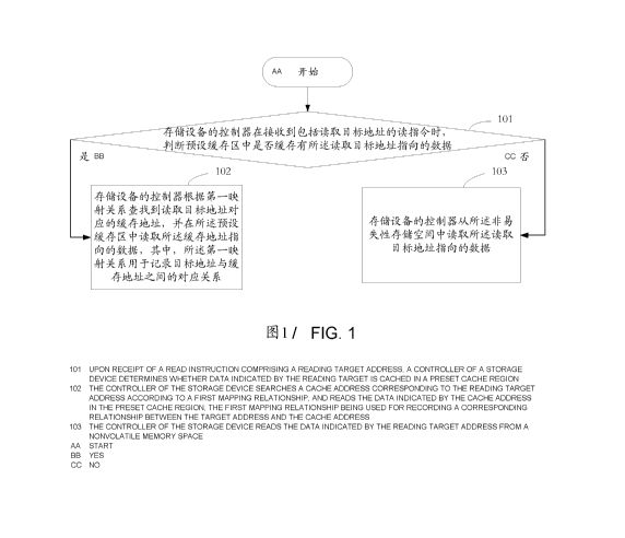
the data is preferentially read from a cache. This avoids the occurrence of an
error in reading the
data due to that the data is currently subject to write interference, thereby
greatly reducing read
errors caused by write interference Moreover, in this implementation manner,
because when data is
being written into an MSB page of a storage device, write interference is
caused only to a shared
page of the MSB page and to a shared page of an adjacent MSB page before the
MSB page, a
manner of dynamically releasing a cache is used, to reduce required cache
space. In addition, in this
application, cache space is allocated according to a maximum page number
difference m of shared
page groups of a storage device, so as to enable compatibility with storage
devices of different
vendors.
[0078] Referring to FIG. 4, FIG. 4 is a partial flowchart of yet
another implementation manner
of a data reading method according to this application. The method in this
implementation manner
includes the steps in the foregoing implementation manner and further includes
the following steps.
[0079] 401. During power-off, the controller of the storage device
saves data that is in the preset
cache area in the non-volatile storage space, and establishes a second mapping
relationship between
the cache address and a save address that is in the non-volatile storage
space.
[0080] After the storage device is powered off, the data in the preset
cache area is lost. To
ensure that the data in the non-volatile storage space can still be correctly
read after next power-on,
during power-off, the controller saves the data that is in the preset cache
area in the non-volatile
storage space, and establishes the second mapping relationship between the
cache address that is in
the preset cache area and the save address that is in the non-volatile storage
space, so that the data
previously cached in the preset cache area can correspond to the data saved in
the non-volatile
storage device.
[0081] 402. During power-on, the controller of the storage device
caches, at the cache address
in the preset cache area according to the second mapping relationship, the
data that the save address
in the non-volatile storage space points to.
[0082] When powered on again, the controller of the storage device
obtains the save address
that is in the non-volatile storage space and that is in the second mapping
relationship, and
correspondingly caches the data at the save address at the cache address that
has the second
mapping relationship with the save address, so as to cache again, according to
the original cache
address, the data that is cached in the preset cache area before power-off. In
this way, when data that
is in the non-volatile storage space and that has been cached needs to be
read, corresponding cached
CA 02971913 2017-06-22
data can be read according to the first. mapping relationship that is
previously established, and
thereby correct data reading is implemented.
[0083] Referring to FIG 5, FIG. 5 is a schematic structural diagram of an
implementation
manner of a data reading apparatus according to this application. In this
implementation manner, the
data reading apparatus 500 may be specifically a controller of a storage
device. The storage device
may be any non-volatile storage device whose floating-gate transistor can
store at least two bits, for
example, an MLC-type or TLC-type SSD. The data reading apparatus 500 includes
a first
determining module 510, a first reading module 520, and a second reading
module 530. The data
reading apparatus 500 is connected to a preset cache area 570 and non-volatile
storage space 580.
[0084] The first determining module 510 is configured to: when receiving a
read instruction that
includes a read target address, determine whether the preset cache area 570
has cached data that the
read target address points to, and send a first determining result to the
first reading module 520 and
the second reading module 530.
[0085] To avoid write interference brought by writing an MSB page,
according to this
application, data that may be subject to the write interference is cached for
backup, and when such a
type of data is read, reading from the preset cache area 570 is preferentially
considered.
[0086] Specifically, for example, the first determining module 510
receives, from a SATA/SAS
interface, a read instruction sent by a host. The read instruction includes a
read target address, so as
to instruct to read, from the non-volatile storage space 580, the data that
the read target address
points to. The first determining module 510 checks whether a first mapping
relationship of the read
target address exists. If the first mapping relationship exists, the first
determining module 510
determines that the preset cache area 570 has cached the data that the read
target address points to.
If the first mapping relationship does not exist, the first determining module
510 determines that the
preset cache area 570 has not cached the data that the read target address
points to.
[0087] It may be understood that, the first determining module 510 may not
determine, by using
the first mapping relationship, whether to-be-read data is cached. In another
implementation
manner, the first determining module 510 may further additionally set an
identifier that records
whether the data at the address is cached. When the data is being read, the
identifier of the address
is read to determine whether the data at the read target address has been
cached. Therefore, a
manner of determining whether to-be-read data has been cached is not
specifically limited herein.
[0088] In addition, when receiving the read instruction, the first
determining module 510 may
further first determine whether the data that the read target address points
to is data subject to write
interference, for example, determine whether the read target address belongs
to an MSB page. If the
read target address does not belong to an MSB page, the first determining
module 510 further
16
CA 02971913 2017-06-22
determines whether the preset cache area 570 has cached the data that the read
target address points
to.
[0089] The
first reading module 520 is configured to: when the preset cache area has
cached the
data that the read target address points to, find a cache address
corresponding to the read target
address according to the first mapping relationship, and read, from the preset
cache area 570, data
that the cache address points to, where the first mapping relationship is used
to record a
correspondence between the target address and the cache address.
[0090]
According to a principle of preferentially reading from a cache, when the
first
determining module 510 determines that the preset cache area 570 has cached
the data that the read
target address points to, the first reading module 520 obtains, according to
the saved first mapping
relationship, the cache address corresponding to the read target address, and
reads the data at the
cache address from the preset cache area 570, so as to implement data reading.
Because data in the
cache area is not subject to write interference as in a storage matrix,
reading data from the cache
area ensures data reading correctness.
[0091] The
second reading module 530 is configured to: when the preset cache area 570 has
not
cached the data that the read target address points to, read, from the non-
volatile storage space 580,
the data that the read target address points to.
100921 When
the first determining module 510 determines that the preset cache area 570 has
not
cached the data that the read target address points to, the second reading
module 530 reads, in a
normal reading
manner, the data at the read target address from the non-volatile storage
space 580,
so as to implement data reading.
[0093]
Optionally, the data reading apparatus 500 in this implementation manner may
further
include a second determining module 540, a first writing module 550, and a
second writing module
560.
[0094] The
second determining module 540 is configured to: when receiving a write
instruction,
determine whether a write target address in the write instruction belongs to
an MSB page in the
non-volatile storage space, and send a second determining result to the first
writing module 550 and
the second writing module 560, where the write instruction includes to be
written data and the write
target address.
10095] The second
determining module 540 receives, from an interface such as a
SATA/SAS/PCIe interface, a write instruction sent by a host. The write
instruction includes to be
written data and a write target address, so as to instruct to store, in the
non-volatile storage space
580 (such as a storage matrix of the storage device) that the write target
address points to, the to be
written data. After receiving the write instruction, the second determining
module 540 first
17
CA 02971913 2017-06-22
determines whether the write target address belongs to an MSB page in the non-
volatile storage
space of the storage device.
[0096] The first writing module 550 is configured to: when it is
determined that the write target
address does not belong to an MSB page in the non-volatile storage space,
store, in the preset cache
area 570 and the non-volatile storage space 580 that is corresponding to the
write target address, the
to be written data, and establish a first mapping relationship between a cache
address and the write
target address.
[0097] When the second determining module 540 determines that the write
target address does
not belong to an MSB page, it means that the to be written data may be subject
to write interference
when data is written into a subsequent MSB page. Therefore, the first writing
module 550 stores, in
the non-volatile storage space 580 that the write target address points to,
the to be written data, and
caches the data into the preset cache area as a backup. The preset cache area
570 may be a DDR or
SRAM in the storage device.
[0098] After the foregoing writing is complete, the first writing module
550 obtains a cache
address at which the to be written data is cached in the preset cache area
570, and establishes a first
mapping relationship between the cache address and the write target address,
so that the data in the
preset cache area 570 corresponds to the data in the non-volatile storage
space 580. The first
mapping relationship may be saved in a tabular form in the non-volatile
storage space 580 of the
storage device or in the preset cache area 570.
[0099] The second writing module 560 is configured to: when it is
determined that the write
target address belongs to an MSB page in the non-volatile storage space,
store, in the non-volatile
storage space 580 corresponding to the write target address, the to be written
data.
[0100] Because an MSB page in the non-volatile storage space is not
subject to write
interference, when the second determining module 540 determines that the to be
written data
.. belongs to an MSB page in the non-volatile storage space, the to be written
data does not need to be
cached for backup, and the data is directly stored in the non-volatile storage
space 580 according to
the write target address.
[0101] In this implementation manner, data for which a read error may
occur due to write
interference of an MSB page is cached for backup. In addition, during reading
of this part of data,
the data is preferentially read from a cache. This avoids the occurrence of an
error in reading the
data due to that the data is currently subject to write interference, thereby
reducing read errors
caused by write interference, and improving reliability of a storage device.
[0102] Referring to FIG 6, FIG. 6 is a schematic structural diagram of
an implementation
manner of a data reading apparatus according to this application.
Specifically, in addition to the
18
CA 02971913 2017-06-22
modules included in the foregoing implementation manner (if a module in FIG. 5
is not mentioned
= in the following description of this implementation manner, the module is
not shown in FIG. 6, but
it does not mean that the data reading apparatus in this implementation manner
does not include the
module), the data reading apparatus 600 further includes a third obtaining
module 610, an allocating
module 620, a third determining module 630, a first obtaining module 640, a
second obtaining
module 650, a releasing module 660, a saving module 670, and a caching module
680.
[0103] The third obtaining module 610 is configured to obtain a maximum
page number
difference m between an MSB page and an LSB page in all groups of shared pages
in the
non-volatile storage space, and send m to the allocating module 620, where m
is a natural number.
[0104] Storage devices of different vendors provide different shared pages.
Using the storage
device shown in Table 1 in the background as an example, the first group of
shared pages in each
block of the storage device is page 0¨page 2. That is, there is a difference
of 2 pages between the
MSB page and the LSB page. The second group of shared pages is page 1¨page 4.
That is, there is a
difference of 3 pages between the MSB page and the LSB page. By traversing all
groups of shared
pages in a block of the storage device, it is found that page number
differences between MSB pages
and corresponding LSB pages are all two or three. Therefore, the maximum page
number difference
between an MSB page and an LSB page in all the groups of shared pages of the
storage device is 3.
[0105] The allocating module 620 is configured to allocate cache space
with a size of at least
n*p+m pages for the preset cache area 570. where p represents a quantity of
shared pages of an
MSB page in the non-volatile storage space, and n is a natural number and is
at least 1.
[0106] To reduce occupation of cache space as much as possible, cache
space for data no longer
subject to write interference is dynamically released in this implementation
manner. A cache space
size required by the preset cache area 570 is related to the maximum page
number difference m
between an MSB page and an LSB page in all the groups of shared pages of the
storage device and
a dynamic release rule.
[0107] According to the foregoing principle for specifying the cache
space size and the
foregoing rule for setting groups of shared pages of the non-volatile storage
space of the storage
device, to ensure that data currently subject to relatively severe write
interference can all be cached,
the allocating module 620 allocates, for the preset cache area, cache space of
at least m+n*p pages,
for example, allocates cache space of m+n*p pages. p represents a quantity of
shared pages of an
MSB page in the non-volatile storage space of the storage device. For example,
one group of shared
pages of an MLC-type storage device includes an MSB page and an LSB page.
Therefore, a
quantity of shared pages of the MSB page in non-volatile storage space of the
storage device is 1,
that is, the LSB page. One group of shared pages of a TLC-type storage device
includes an MSB
19
CA 02971913 2017-06-22
, page. a CSB page, and an LSB page. T,herefor,e, a quantity of shared pages
of the MSB page in
non-volatile storage space of the storage device is 2, including the CSB page
and the LSB page.
[0108] The third determining module 630 is configured to: when the write
target address
belongs to an MSB page in the non-volatile storage space, determine whether
the MSB page in
which the write target address is located is the last MSB page in a block
block, and send a third
determining result to the first obtaining module 640 and the second obtaining
module 650.
[0109] For example, when the second determining module 540 determines
that the write target
address belongs to an MSB page in the non-volatile storage space, the third
determining module
630 determines whether the MSB page in which the write target address is
located is the last MSB
page in the block.
[0110] The first obtaining module 640 is configured to: when the MSB
page in which the write
target address is located is not the last MSB page in the block, obtain an
address of a shared page of
the nth MSB page as counted forward from the MSB page in which the write
target address is
located, use the obtained address as a data release address, and send the data
release address to the
releasing module 660.
[0111] In this implementation manner, a dynamic cache release manner is
used. A specific rule
is that, when data is being written into an MSB page, it is ensured that
shared pages of at least n
MSB pages (such as LSB pages or CSB pages corresponding to the MSB pages) can
be cached in a
preset cache area. Using the MLC-type storage device shown in Table 2 in the
background as an
example, it can be known from Table 2 that an LSB page is subject to
relatively severe write
interference in a process between writing an MSB page corresponding to the LSB
page and starting
writing a next MSB page. It can be ensured that data currently subject to
relatively severe write
interference can all be cached, only when a minimum value of n is 1. However,
to further reduce
read interference, n is preferentially at least 2. That is, an LSB page
corresponding to an MSB page
is not deleted before writing of data into at least two MSB pages next to the
MSB page is complete.
[0112] Specifically, still using the storage device described in Table 1
in the background as an
example, it is assumed that a current write target address belongs to page 6,
which is an MSB page,
and does not belong to the last MSB page. As counted forward from page 6, the
first MSB page is
page 4, and the second MSB page is page 2. If n is 1, it is considered that no
write interference will
be caused to a shared page of page 4, that is. page 1, after data is written
into page 6. Therefore, the
first obtaining module 640 uses an address of page 1 as a data release
address, so as to release cache
space that is in the preset cache area 570 and that is corresponding to page
1.
[0113] It is the same for a storage device whose floating-gate
transistor stores more than two
bits. That is, addresses of shared pages (if the floating-gate transistor
stores three bits, a
CA 02971913 2017-06-22
corresponding LSB page and a corresponding CSB page are included) of the nth
MSB page as
counted forward from the MSB page in which the write target address is located
are obtained and
used as data release addresses.
[0114] The second obtaining module 650 is configured to: when the MSB
page in which the
write target address is located is the last MSB page in the block, obtain
addresses of shared pages of
the last n+1 MSB pages in the block, use the obtained addresses as the data
release addresses, and
send the data release addresses to the releasing module 660.
[0115] If the MSB page in which the write target address is located is
the last MSB page in the
block, it means that write interference of all pages in the block is
eliminated, and therefore all data
cache space of the block can be released. According to the cache release rule
of the foregoing first
obtaining module 640, when data is being written into the last MSB page, data
of shared pages of
the last n+1 MSB pages in the block remains cached in the preset cache area,
where n is a natural
number and is at least 1. Therefore, the second obtaining module 650 obtains
the addresses of the
shared pages (which are LSB pages if the floating-gate transistor stores two
bits, or include LSB
.. pages and CSB pages if the floating-gate transistor stores three bits) of
the last n+1 MSB pages in
the block, and uses the obtained addresses as the data release addresses.
[0116] The releasing module 660 is configured to release data that is in
the preset cache area
and that a cache address having the first mapping relationship with the data
release address points to,
and delete the data release address from the first mapping relationship.
[0117] The releasing module 660 obtains, according to the first mapping
relationship, the cache
address having the first mapping relationship with the data release address,
and releases the data at
the cache address. In this way, cache space can be dynamically released while
ensuring that data
currently subject to severe write interference remains cached. Because the
cache space is already
released, the data release address and the cache address in the first mapping
relationship are deleted.
[0118] The saving module 670 is configured to: during power-off, save data
that is in the preset
cache area 570 in the non-volatile storage space, establish a second mapping
relationship between
the cache address and a save address that is in the non-volatile storage
space, and send the second
mapping relationship to the caching module 680.
[0119] After the storage device is powered off, the data in the preset
cache area 570 is lost. To
.. ensure that the data in the non-volatile storage space can still be
correctly read after next power-on,
during power-off, the saving module 670 saves the data that is in the preset
cache area in the
non-volatile storage space, and establishes the second mapping relationship
between the cache
address that is in the preset cache area and the save address that is in the
non-volatile storage space,
so that the data previously cached in the preset cache area can correspond to
the data saved in the
21
CA 02971913 2017-06-22
s non-volatile storage device.
[0120] The caching module 680 is configured to: during power-on, cache,
at the cache address
in the preset cache area 570 according to the second mapping relationship, the
data that the save
address in the non-volatile storage space points to.
[0121] When powered on again, the caching module 680 obtains the save
address that is in the
non-volatile storage space and that is in the second mapping relationship, and
correspondingly
caches the data at the save address at the cache address that has the second
mapping relationship
with the save address, so as to cache again, according to the original cache
address, the data that is
cached in the preset cache area before power-off. In this way, when data that
is in the non-volatile
storage space and that has been cached needs to be read, corresponding cached
data can be read
according to the first mapping relationship that is previously established,
and thereby correct data
reading is implemented.
[0122] It may be understood that, the data reading apparatus in this
application is limited to
including all the modules in this implementation manner. In a different
implementation manner, in
addition to the modules shown in FIG. 5, the data reading apparatus may
further include only the
third obtaining module and the allocating module, or further include only the
third determining
module, the first obtaining module, the second obtaining module, and the
releasing module, or
further include only the saving module and the caching module, or further
include modules of two
of the three alternatives.
[0123] Referring to FIG. 7, FIG. 7 is a schematic structural diagram of an
implementation
manner of a controller according to this application. The controller 700 in
this implementation
manner includes a receiver 701, a processor 702, a memory 703, and a bus 704.
The controller 700
is connected to a preset cache area 710 and non-volatile storage space 720.
101241 The receiver 701 is configured to receive a write instruction and
a read instruction.
[0125] The processor 702 is configured to:
when receiving a read instruction that includes a read target address,
determine whether
the preset cache area 710 has cached data that the read target address points
to; and
when the preset cache area has cached the data that the read target address
points to, find
a cache address corresponding to the read target address according to a first
mapping relationship,
and read, from the preset cache area 710, data that the cache address points
to, where the first
mapping relationship is used to record a correspondence between the target
address and the cache
address; or when the preset cache area has not cached the data that the read
target address points to,
read, from the non-volatile storage space 720, the data that the read target
address points to.
[0126] Optionally, the processor 702 may be further configured to:
22
CA 02971913 2017-06-22
when receiving a write instruction, determine whether a write target address
in the write
instruction belongs to a most significant bit page MSB page in the non-
volatile storage space 720,
where the write instruction includes to be written data and the write target
address; and
when it is determined that the write target address does not belong to an MSB
page in
the non-volatile storage space, store, in the preset cache area 710 and the
non-volatile storage space
720 that is corresponding to the write target address, the to be written data,
and establish a first
mapping relationship between a cache address and the target address; or when
it is detei mined that
the write target address belongs to an MSB page in the non-volatile storage
space, store, in the
non-volatile storage space 720 corresponding to the write target address, the
to be written data.
[0127] Optionally, the processor 702 is further configured to:
when the write target address belongs to an MSB page in the non-volatile
storage space
720, determine whether the MSB page in which the write target address is
located is the last MSB
page in a block block;
when the MSB page in which the write target address is located is not the last
MSB page
in the block, obtain an address of a shared page of the nth MSB page as
counted forward from the
MSB page in which the write target address is located, and use the obtained
address as a data
release address, where n is a natural number and is at least 1; or the second
obtaining module is
configured to: when the MSB page in which the write target address is located
is the last MSB page
in the block, obtain addresses of shared pages of the last n+1 MSB pages in
the block, and use the
obtained addresses as the data release addresses, where n is a natural number
and is at least I; and
release data that is in the preset cache area 710 and that a cache address
having the first
mapping relationship with the data release address points to, and delete the
data release address
from the first mapping relationship.
[0128] Optionally, the processor 702 is further configured to:
obtain a maximum page number difference m between an MSB page and an LSB page
in all groups of shared pages in the non-volatile storage space 720, where m
is a natural number;
and
allocate cache space with a size of at least n*p+m pages for the preset cache
area 710,
where p represents a quantity of shared pages of an MSB page in the non-
volatile storage space 720,
and n is a natural number and is at least 1.
101291 Optionally, the processor 702 is further configured to:
during power-off, save data that is in the preset cache area 710 in the non-
volatile
storage space 720, and establish a second mapping relationship between the
cache address and a
save address that is in the non-volatile storage space 720; and
23
CA 02971913 2017-06-22
during power-on, cache, at the cache address in the preset cache area 710
according to
the second mapping relationship, the data that the save address in the non-
volatile storage space 720
points to.
[0130]
The memory 703 may include a read-only memory and a random access memory, and
provide instructions and data for the processor 702. A part of the memory 703
may further include a
non-volatile random access memory (NVRAM). In another implementation manner,
the memory
703 may alternatively be located in a same storage medium with the non-
volatile storage space 610.
[0131]
The memory 703 stores the following elements, executable modules or data
structures, a
subset thereof, or an extension set thereof:
operating instructions: including various operating instructions used to
implement
various operations; and
an operating system: including various system programs, which are used to
implement
various basic services and process hardware-based tasks.
101321
In an embodiment of the present invention, the processor 702 executes the
foregoing
operations by calling the operating instructions stored in the memory 703 (the
operating instructions
may be stored in the operating system).
[0133]
The processor 702 may also be referred to as a CPU (Central Processing Unit,
central
processing unit). In a specific application, components of the controller are
coupled together by
using the bus 704. The bus 704 includes a data bus, and in addition, may
further include a power
bus, a control bus, a state signal bus, and the like. However, for clarity of
description, various buses
are marked as the bus 704 in the figure.
[0134]
The method disclosed in the foregoing embodiments of the present invention
may be
applied to the processor 702, or implemented by the processor 702. The
processor 702 may be an
integrated circuit chip and has a signal processing capability. In an
implementation process. the
steps of the foregoing methods may be completed by using a hardware integrated
logic circuit of the
processor 702 or software instructions. The processor 702 may be a general-
purpose processor, a
digital signal processor (DSP), an application-specific integrated circuit
(ASIC), a field
programmable gate array (FPGA) or another programmable logical device, a
discrete gate or a
transistor logic device, or a discrete hardware component. The methods, steps,
and logical block
diagrams disclosed in the embodiments of the present invention can be
implemented or executed.
The general-purpose processor may be a micro processor, or the processor may
be any conventional
processor or the like. The steps of the methods disclosed in the embodiments
of the present
invention may be directly executed by a hardware decoding processor, or
executed by a
combination of hardware in a decoding processor and software modules. The
software modules may
24
CA 02971913 2017-06-22
be located in a storage medium mature in the art, such as a random access
memory, a flash memory,
= a read-only memory, a programmable read-only memory, an electrically
erasable programmable
memory, or a register. The storage medium is located in the memory 703. The
processor 702 reads
information from the memory 703, and implements the steps of the foregoing
methods in
combination with the hardware of the processor 702.
[0135] In the foregoing solution, data that is in storage space and
that is of a page susceptible to
a data read error due to write interference is cached in a preset cache area,
and when the data of the
page is read, the data is selectively read from the cache area, so as to avoid
reading data that may
contain an error from the storage space. This reduces data read errors caused
by write interference,
and improves reliability of a storage device.
[0136] In the several embodiments provided in this application, it
should be understood that the
disclosed system, apparatus, and method may be implemented in other manners.
For example, the
described apparatus embodiment is merely exemplary. For example, the module or
unit division is
merely logical function division and may be other division in an actual
implementation. For
example, a plurality of units or components may be combined or integrated into
another system, or
some features may be ignored or not performed. In addition, the displayed or
discussed mutual
couplings or direct couplings or communication connections may be indirect
couplings or
communication connections between interfaces, apparatuses, and units, or may
be implemented in
electronic, mechanical, or other forms.
[0137] The units described as separate parts may or may not be physically
separate. Parts
displayed as units may or may not be physical units, and may be located in one
location, or may be
distributed on a plurality of network units. Some or all of the units may be
selected according to
actual requirements to achieve the objectives of the solutions of the
embodiments.
[0138] In addition, functional units in the embodiments of this
application may be integrated
into one processing unit, or each of the units may exist alone physically, or
two or more units are
integrated into one unit. The integrated unit may be implemented in a form of
hardware, or may be
implemented in a form of a software functional unit.
[0139] When the integrated unit is implemented in the form of a
software functional unit and
sold or used as an independent product, the integrated unit may be stored in a
computer-readable
storage medium. Based on such an understanding, the technical solutions of
this application
essentially, or the part contributing to the prior art, or all or a part of
the technical solutions may be
implemented in the form of a software product. The software product is stored
in a storage medium
and includes several instructions for instructing a computer device (which may
be a personal
computer, a server, or a network device) or a processor (processor) to perform
all or a part of the
CA 02971913 2017-06-22
steps of the methods described in the implementation manners of this
application. The foregoing
storage medium includes: any medium that can store program code, such as a USB
flash drive, a
=
removable hard disk, a read-only memory (ROM, Read-Only Memory), a random
access memory
(RAM. Random Access Memory), a magnetic disk, or an optical disc.
26