Note: Descriptions are shown in the official language in which they were submitted.
MULTI-STAGE MULTILEVEL DC-DC STEP-DOWN CONVERTER
Related Applications
This application claims the benefit of the filing date of U.S. Application.No.
62/446,516,
filed January 15, 2017, and U.S. Application No. 62/359,265, filed July 7,
2016, the contents of
which are incorporated herein by reference in their entirety.
Field
This invention relates to DC¨DC converters. More specifically, this invention
provides
multi-stage multilevel DC¨DC converter architectures that reduce voltage
stress on switches
and inductors, reduce the size of the converter, increase power density, and
improve efficiency.
Background
Previously, 12V DC bus voltage has been widely used for motherboards of
servers in
applications such as data centers. More recently, 48V power distribution has
been used, which
can provide better efficiency and performance for the high power demands of
computing
systems in data centres. In current 48V rack-level UPS systems, 48V is
directly provided to the
motherboards in servers and is converted down in one stage, using one power
converter, or
one power conversion stage, to a lower voltage level required by CPUs and
GPUs, such as from
1V to 3.3V.
Multi-phase Buck point-of-load (POL) converters, as shown in Fig. 1, are the
dominant
architecture of step down converters in applications for converting 48V to a
much lower
voltage level (e.g., 1V to 3.3V). As the required inductance value of the Buck
converter is
directly proportional to the voltage difference between the input and output
of the converter,
the inductance value increases with increasing voltage difference (such as
from 48V to 1V).
Accordingly, the volume of the inductors in Buck converter will increase as
well, which lowers
power density. Additionally, the 48V input voltage increases voltage stress on
the switches
which leads to higher switching losses. Therefore, there are drawbacks to
current approaches
for implementing 48V DC bus architecture in applications such as motherboards
of servers.
1
CA 2972307 2017-07-06
Summary
Disclosed are multi-stage multilevel DC-DC step-down converters. In various
embodiments, stages may include three or four switches, and switches of each
stage are
operated at selected duty cycles such that each stage reduces an input voltage
by one-half,
voltage stress on switches is reduced, and an output inductor may be very
small as compared
with a conventional Buck converter.
According to one aspect, there is provided a method for controlling a DC-DC
converter,
wherein the DC-DC converter comprises at least one stage, wherein the at least
one stage is a
first stage comprising: first and second input terminals and first and second
output terminals,
wherein the second input terminal and the second output terminal are connected
together as a
common terminal; first, second, third, and fourth switches connected together
in series across
the first and second input terminals; a first capacitor connected in parallel
with the second and
third switches; a first inductor having a first terminal connected between the
second and third
switches and a second terminal connected to a first output terminal; and a
second capacitor
connected across the first and second output terminals;
wherein the method comprises: turning on the first and third switches for a
first
selected portion of a first switching cycle; turning on the second and fourth
switches for a
second selected portion of the first switching cycle; wherein the first and
second selected
portions of the first switching cycle are each 50%; wherein an output DC
voltage of the DC-DC
converter is 0.5 times an input DC voltage of the DC-DC converter; and wherein
a voltage across
the first inductor is substantially zero volts.
In one embodiment, a DC-DC converter may comprise a second stage; wherein the
second stage comprises fifth, sixth, seventh, and eighth switches connected
together in series, a
second stage first input terminal connected to an input terminal of the fifth
switch, a second
stage first output terminal connected to a point between the sixth and seventh
switches, and a
third capacitor connected in parallel with the sixth and seventh switches;
wherein the second
stage first input terminal is connected between the second and third switches
and the second
stage first output terminal is connected to the first terminal of the first
inductor;
2
CA 2972307 2017-07-06
wherein the method comprises: turning on the first and third switches for a
first 25% of
a first switching cycle at a first switching frequency; turning on the second
and fourth switches
for a second 25% of the first switching cycle at the first switching
frequency; turning on the fifth
and seventh switches for a first 50% of a first switching cycle at a second
switching frequency;
turning on the sixth and eighth switches for a second 50% of the first
switching cycle at the
second switching frequency; wherein an output DC voltage of the DC-DC
converter is 0.25 times
an input DC voltage of the DC-DC converter; and wherein a voltage across the
first inductor is
substantially zero volts and a voltage across the second inductor is
substantially zero volts.
In one embodiment, a DC-DC converter may comprise a second stage connected
between the second capacitor of the first stage and the output terminals;
wherein the second
stage comprises fifth, sixth, seventh, and eighth switches connected together
in series across
the second capacitor; a third capacitor connected in parallel with the sixth
and seventh
switches; a second inductor having a first terminal connected between the
sixth and seventh
switches and a second terminal connected to the first output terminal; and a
fourth capacitor
connected across the first and second output terminals;
wherein the method comprises: turning on the first and third switches for a
first 50% of
a first switching cycle at a first switching frequency; turning on the second
and fourth switches
for a second 50% of the first switching cycle at the first switching
frequency; turning on the fifth
and seventh switches for a first 50% of a first switching cycle at a second
switching frequency;
turning on the sixth and eighth switches for a second 50% of the first
switching cycle at the
second switching frequency; wherein an output DC voltage of the DC-DC
converter is 0.25 times
an input DC voltage of the DC-DC converter; and wherein a voltage across the
first inductor is
substantially zero volts and a voltage across the second inductor is
substantially zero volts.
In one embodiment, a DC-DC converter may comprise a second stage connected
between the third and fourth switches of the first stage and the first
inductor; wherein the
second stage comprises fifth, sixth, and seventh switches connected together
in series across
the third and fourth switches; a third capacitor connected in parallel with
the fifth and sixth
switches; wherein the first terminal of the first inductor is connected
between the fifth and
3
CA 2972307 2017-07-06
sixth switches and the second terminal of the first inductor is connected to
the first output
terminal; and the second capacitor is connected across the first and second
output terminals;
wherein the method comprises: turning on the first and third switches for a
first 25% of
a switching cycle; turning on the second and fourth switches for a second 25%
of the switching
cycle; turning on the fifth and seventh switches for a first 50% of the
switching cycle; turning on
the sixth switch for a second 50% of the switching cycle; wherein an output DC
voltage of the
DC-DC converter is 0.25 times an input DC voltage of the DC-DC converter; and
wherein a
voltage across the first inductor is substantially zero volts.
In one embodiment, a DC-DC converter may comprise a third stage connected
between
the sixth and seventh switches of the second stage and the first inductor;
wherein the third
stage comprises eighth, ninth, and tenth switches connected together in series
across the sixth
and seventh switches; a fourth capacitor connected in parallel with the eighth
and ninth
switches; wherein the first terminal of the first inductor is connected
between the eighth and
ninth switches and the second terminal of the first inductor is connected to
the first output
terminal; and the second capacitor is connected across the first and second
output terminals;
wherein the method comprises: turning on the first and third switches for a
first 12.5%
of a switching cycle; turning on the second and fourth switches for a second
12.5% of the
switching cycle; turning on the fifth and seventh switches for a first 25% of
the switching cycle;
turning on the sixth switch for a second 25% of the switching cycle; turning
on the eighth and
ninth switches for a first 50% of the switching cycle; turning on the tenth
switch for a second
50% of the switching cycle; wherein an output DC voltage of the DC-DC
converter is 0.125 times
an input DC voltage of the DC-DC converter; and wherein a voltage across the
first inductor is
substantially zero volts.
In various embodiments, the first switching frequency and the second switching
frequency are different; or the first switching frequency and the second
switching frequency
are the same and a phase of the first stage and a phase of the second stage
are different, or the
first switching frequency and the second switching frequency are the same and
a phase of the
first stage and a phase of the second stage are the same.
4
CA 2972307 2017-07-06
In various embodiments, the method may include controlling a dead time of
switches of
one or more stages, wherein controlling the dead time minimizes a volt-second
produced
across the first inductor for a duration of the dead time. The duration of the
dead time may be
controlled to be less than 200 nanoseconds.
According to another aspect of the invention, there is provided a DC-DC
converter,
comprising: a first input terminal adapted to receive an input DC voltage; a
common terminal; a
first four switch (45) stage comprising: first, second, third, and fourth
switches connected
together in series across the first input terminal and the common terminal; a
first capacitor
connected in parallel with the series-connected second and third switches; a
4S input point
connected to an input terminal of the first switch; a 4S output point at a
first node between the
second and third switches; a common terminal connected to an output terminal
of the fourth
switch; an output circuit comprising a series inductor, a parallel capacitor,
and a first output
terminal adapted to output a DC voltage; and a controller that controls the 4S
switches such
that the first and third switches are switched on and off together, the second
and fourth
switches are switched on and off together, the first and third switches are
not on when the
second and fourth switches are on, and the duty cycle of the switches is 50%
or less; wherein an
output DC voltage is one-half of the input DC voltage.
In one embodiment, a DC-DC converter may comprise a second 4S stage; wherein
the
second 4S stage comprises fifth, sixth, seventh, and eighth switches connected
together in
series, a second 45 stage first input point connected to an input terminal of
the fifth switch, a
second 4S stage first output point connected between the sixth and seventh
switches, and a
third capacitor connected in parallel with the sixth and seventh switches;
wherein the second
45 stage first input point is connected between the second and third switches
and the second
45 stage first output point is connected to a first terminal of the series
inductor; a controller
that controls the first 4S stage switches and the second 45 stage switches
such that: the first
and third switches are switched on and off together for a first 25% of a first
switching cycle at a
first switching frequency; the second and fourth switches are switched on and
off together for a
second 25% of the first switching cycle at the first switching frequency; the
fifth and seventh
5
CA 2972307 2017-07-06
switches are switched on and off together for a first 50% of a first switching
cycle at a second
switching frequency; and the sixth and eighth switches are switched on and off
together for a
second 50% of the first switching cycle at the second switching frequency;
wherein an output
DC voltage of the DC-DC converter is 0.25 times an input DC voltage of the DC-
DC converter;
and wherein a voltage across the series inductor is substantially zero volts.
In one embodiment, a DC-DC may comprise a 4S stage and a three switch (3S)
stage,
wherein the 35 stage comprises: fifth, sixth, and seventh switches connected
together in series;
a 3S input point connected to an input terminal of the fifth switch; a 35
output point connected
to an output terminal of the fifth switch; a second capacitor connected in
parallel with the
series-connected fifth and sixth switches; and a common terminal connected to
an output
terminal of the seventh switch; wherein the 35 input point is connected to the
45 output point
of the 4S stage, and the 35 output point is connected to the output circuit;
wherein the
controller controls the 45 switches such that the duty cycle is 25%; and
wherein the controller
controls the 3S switches such that the fifth and seventh switches are switched
on and off
together, the sixth switch is switched on and off, the fifth and seventh
switches are not on
when the sixth switch is on, and the duty cycle of the 3S switches is
50%;wherein an output DC
voltage is one-quarter of the input DC voltage.
In one embodiment, a DC-DC converter may comprise a 4S stage and first and
second 35
stages; wherein the first and second 3S stages are cascaded by connecting the
first 3S stage
output point to the second 3S stage input point; wherein the first 35 stage
input point is
connected to the 45 output point of the 45 stage, and the second 3S stage
output point is
connected to the output circuit; wherein the controller controls the 4S
switches such that the
duty cycle is 12.5%; and wherein the controller controls the first 35 stage
such that the duty
cycle is 25%; wherein the controller controls the second 35 stage such that
the duty cycle is
50%; wherein an output DC voltage is one-eighth of the input DC voltage.
In one embodiment, a DC-DC converter may comprise a 45 stage and three or more
35
stages; wherein the three or more 35 stages are cascadable by connecting a
first 3S stage
output point to a second 3S stage input point, connecting a second 3S stage
output point to a
6
CA 2972307 2017-07-06
third 35 stage input point, and continuing to a final 35 stage; wherein the
first 3S stage input
point is connected to the 4S output point of the 4S stage, and the final 3S
stage output point is
connected to the output circuit; wherein a total number of stages is N;
wherein the controller
controls switches of the Nth stage such that the duty cycle is 50%, and
controls the switches of
each preceding stage such that the duty cycle decreases by half for each
preceding stage;
wherein the output DC voltage is equal to the input DC voltage divided by 2".
In various embodiments, the controller further comprises a dead time control
circuit,
wherein the controller controls duration of the dead time to be less than 200
nanoseconds.
In various embodiments, the controller controls the first switching frequency
and the
second switching frequency to be different; or controls the first switching
frequency and the
second switching frequency to be the same and a phase of the first stage and a
phase of the
second stage to be different, or controls the first switching frequency and
the second switching
frequency to be the same and a phase of the first stage and a phase of the
second stage to be
the same.
Brief Description of the Drawings
For a greater understanding of the invention, and to show more clearly how it
may be
carried into effect, embodiments will be described, by way of example, with
reference to the
accompanying drawings, wherein:
Fig. 1 is a circuit diagram of a multi-phase Buck point-of-load (POL)
converter, according
to the prior art.
Fig. 2A is a circuit diagram of a multi-stage multilevel DC¨DC step-down
converter,
according to one embodiment.
Fig. 2B is a circuit diagram of a 4S cell for use in DC¨DC step-down
converters according
to embodiments described herein.
Fig. 2C is a circuit diagram of a 3S cell for use in DC¨DC step-down
converters according
to embodiments described herein.
7
CA 2972307 2017-07-06
Figs. 3 and 4 are circuit diagrams of a two-stage DC¨DC step-down converter,
according
to one embodiment.
Fig. 5 is a timing diagram for the switches of the circuit of Fig. 3 and 4,
during one
switching cycle Ts.
Figs. 6, 7, and 8 are equivalent circuits for the two-stage DC¨DC step-down
converter of
Fig. 4 during three operating states that make up one switching cycle, as
shown in Fig. 5: State 1
(from to to t1), State 2 (from t1 to t2), and State 3 (from t2 to Ts),
respectively.
Fig. 9 is an equivalent circuit for the two-stage DC¨DC step-down converter of
Fig. 4
during a dead time operating mode.
Figs. 10, 11, and 12 show simulation results for the circuit of Fig. 3 or 4,
wherein Fig. 10
shows capacitor voltages and current, Fig. 11 shows current waveforms for all
the switches, and
Fig. 12 shows inductor voltage and current waveforms.
Fig. 13 shows simulated voltage waveforms at nodes Ni and N2 (upper and lower
panels, respectively) for the embodiment of Fig. 4.
Fig. 14 shows simulated drain to source voltage waveforms for each switch (M1
¨ M7) of
the embodiment of Fig. 4, wherein the waveforms (from top to bottom) are
Vds_M1, Vds_M2,
Vds_M3, Vds_M4, Vds_M5, Vds_M6, and Vds_M7.
Fig. 15 is a diagram of a three stage DC¨DC converter, including one 4S cell
and two 3S
cells, according to one embodiment.
Fig. 16 is a diagram of a two-stage DC¨DC converter using two 45 cells
connected in
cascade, according to one embodiment.
Fig. 17 is a timing diagram for the embodiment of Fig. 4, where it can be seen
that the
instantaneous voltage across the inductor Lo is zero all the time, as shown in
Fig. 17 the bottom
waveform.
8
CA 2972307 2017-07-06
Fig. 18 is a diagram of a two stage zero inductor voltage DC¨DC converter with
a voltage
transfer ratio of 1/4, according to one embodiment.
Fig. 19 is a diagram of a three stage zero inductor voltage DC¨DC converter
with a
voltage transfer ratio of 1/8, according to one embodiment.
Fig. 20 is a diagram of a single-stage three-level step-down converter
including a 45 cell,
an LC filter, and a 50% duty cycle controller.
Fig. 21 shows simulation waveforms for the embodiment of Fig. 20, wherein the
waveforms are (top to bottom) the gate drive signal for M1 and M3 (Vgs1 and
Vgs3), the gate
drive signal for M2 and M4 (Vgs2 and Vgs4), the inductor voltage waveform
(VLo), the voltage
at node Ni (VN1) and the output voltage (Vout), and the capacitor voltage VC1.
Fig. 22 shows an embodiment wherein two zero inductor voltage three level
converters
are connected in series in cascade mode to achieve a four times voltage step
down ratio,
including two 4s cells and two LC filters, and 50% duty cycle controllers.
Fig. 23 is a diagram of a zero inductor voltage seven switch converter (e.g.,
as in Fig. 4)
and a fixed duty cycle controller including a dead time control circuit.
Fig. 24 is a diagram of a zero inductor voltage three level converter as in
Fig. 20, with a
50% fixed duty cycle controller including a dead time control circuit.
Fig. 25 shows simulated inductor voltage (top) and inductor current (bottom)
waveforms for the DC¨DC converter circuit of Fig. 23, when dead time is
considered
Fig. 26 shows simulated inductor voltage (top) and inductor current (bottom)
waveforms for the DC¨DC converter circuit of Fig. 24, when dead time is
considered.
Fig. 27 shows the simulated output impedance of a zero inductor voltage seven
switch
converter embodiment of Fig. 18, wherein the upper plot is the magnitude of
the output
impedance and the lower plot is the phase of the output impedance.
9
CA 2972307 2017-07-06
Detailed Description of Embodiments
Provided herein are multi-stage multilevel DC¨DC step-down converters which
overcome the drawbacks of prior approaches. As described herein, embodiments
employ
multi-stage multilevel architectures which reduce voltage stress on switches
and inductors,
reduce the size of the converter on the motherboard, thereby increasing power
density, and
improve efficiency of the power system. Embodiments are suitable for use in
servers, and,
because of their improved efficiency and high power density, they are
particularly suitable for
use in server-intense environments such as data centers. However, it will be
appreciated that
embodiments may also be used in other applications.
Also provided herein are methods for implementing multi-stage multilevel DC¨DC
step-
down converters which overcome the drawbacks of prior approaches. As described
herein, the
methods provide multi-stage multilevel architectures which reduce voltage
stress on switches
and inductors, reduce the size the converter on the motherboard, thereby
increasing power
density, and improve efficiency of the power system. The methods are
applicable to servers,
and, because they improve efficiency and increase power density, they may be
implemented in
server-intense environments such as data centers, although they are not
limited thereto.
As used herein, the term "switch" is intended to refer to a semiconductor
switch where
the current can flow in both directions and withstand voltage in one
direction, such as IGBT
with a parallel diode, or MOSFET where the parallel diode is inherent.
Throughout this disclosure, where a value is given, such as, for example, OV,
50%, etc., it
will be appreciated that the value may be a theoretical or design value and
slight variation may
be expected in a practical implementation due to factors such as component
tolerances, ripple,
etc. Such variation is intended to be covered by the embodiments described
herein. In some
instances the terms "substantially" or "approximately" may be used in respect
of a value, and
are intended to mean a value in a practical implementation that is exactly or
close to a
theoretical value, given practical limitations.
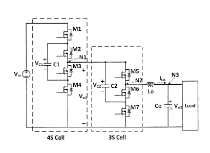
A multi-stage multilevel DC-DC step-down converter will now be described with
reference to Fig. 2A. This embodiment includes multiple stages which are
connected in
CA 2972307 2017-07-06
cascade. The first stage, referred to as a 4S cell, has four switches (M1, M2,
M3, and M4)
connected in series and one flying capacitor (Cl) connected across the middle
of two switches
(drain of M2 and source of M3). The input of the first stage (45 cell) is the
drain of the first
switch Ml, which is connected to the input voltage V. Fig. 2B shows the
topology of the 45
cell. The output of the 45 cell is the source of switch M2 (which is connected
to the drain of the
third switch, M3), shown as point Ni in Fig. 2A, or OUT_45 in Fig. 2B. The
source terminal of
M4 is the common (or ground) connection of the 4S cell, which is connected to
the negative
terminal of Vin.
As shown in Fig. 2A, the first stage (4S cell) is followed by one or more
further stages,
referred to as 3S cells. Each 3S cell has three series connected switches
(such as M5, M6, M7 as
shown in Figs. 2A and 2C) and one flying capacitor (such as C2 as shown in
Figs. 2A and 2C). In
each 35 cell the positive terminal of the flying capacitor C2 is connected to
the drain of the first
switch M5. The negative terminal of the flying capacitor is connected to the
source of the
second switch M6. The source of the third switch M7 is connect to the common
terminal,
which is the negative terminal of \tin, or ground. The input of the 35 cell is
at the drain of the
first switch M5. The output of the 3S cell is at the source of the first
switch M5, as shown as
point N2 in Fig. 2A.
An LC filter, including series inductor Lo and parallel capacitor Co, is
connected at the
output of the last 35 cell, as shown in Fig. 2A. The load is connected in
parallel with the filter
capacitor Co. The load may be another DC¨DC converter (such as, for example, a
Buck
converter) or a resistor, or any other device.
The total number of switches is 4 + 3*(N-1) where N represents the number of
stages.
The total number of flying capacitors is N. For example, a two-stage converter
(N = 2), as
shown in Fig. 3, has 4 + 3*(2-1) = 7 switches.
According to the embodiments, each stage steps down the input voltage by one-
half.
Therefore, the output voltage of an N stage converter is Vo = V1/2N. For a two
stage converter,
as shown in Fig. 3, N = 2, and Vo2 = Vin/4. For a three stage converter, the
first stage will be a
45 cell, the second stage will be a 3S cell, and the third stage will be a 3S
cell. The output
11
CA 2972307 2017-07-06
voltage Vo3 is Vin/8.It will be appreciated that the voltage stress on the
switches of the Nth
stage is reduced to V1n/2N. More detailed analysis will be provided in the
following sections.
Two-Stage Multilevel DC-DC Step-Down Converter
Circuit Configuration
A two-stage (N = 2) multilevel DC¨DC step-down converter as shown in the
embodiment
of Figs. 3 and 4 will be analyzed as an example. In this embodiment, the first
stage is a 45 cell
and the second stage is a 35 cell, as shown by the dashed lines in Fig. 3.
Further description will
be made with reference to Fig. 4. With a two stage configuration, the output
voltage Vo2
equals to V1n/22= Vin/4. For example, 48V input voltage is reduced to 12V at
the output. The
load is connected to the point N3, as shown in Fig. 4. The 4S cell includes a
first switch M1, a
second switch M2, a third switch M3, and a fourth switch M4. The 3S cell
includes a fifth switch
M5, a sixth switch M6, and a seventh switch M7.
The input terminal of the 4S cell (the drain of M1) is connected to the
positive terminal
of the input voltage yin. The source of M1 is connected to both the positive
terminal of the first
flying capacitor C1 and the drain of the second switch M2. The source of M2 is
connected to
the drain of the third switch M3. The source of the third switch M3 is
connected to both the
negative terminal of the first flying capacitor (C1) and the drain of the
fourth switch M4. The
source of M4 is connected to the common terminal and the negative terminal of
Vin. The input
of the 45 cell is the drain of the first switch Ml. The output of the 4S cell
is the source of the
second switch M2, which is also the source of the third switch M3. The output
of the 45 cell is
indicated by point Ni in Fig. 4. The output of the 4S cell is connected to the
input of the 3S cell.
In the 3S cell, the positive terminal of the second flying capacitor C2 is
connected to the
drain of the fifth switch M5. The source of the fifth switch is connected to
the drain of the sixth
switch M6. The source of the sixth switch M6 is connected to both the negative
terminal of the
second flying capacitor CZ and the drain of the seventh switch M7. An LC
filter is connected to
the output of the 3S cell and provides DC voltage to the load.
12
CA 2972307 2017-07-06
The output of the 4S cell (point Ni) is connected to the input of the 3S cell
(drain of M5),
as shown in Fig. 4. The inductor of the output LC filter is connected to the
output of the 3S cell
(point N2 as shown in Fig. 4) and the load is connected in parallel with the
output capacitor Co.
Operating Principle
For the purpose of this description, the term Vci refers to the first flying
capacitor
voltage, VC2 refers to the second flying capacitor voltage, Vi, refers to the
power supply input
voltage, V.1 refers to the output voltage from the first stage of converter
(4S cell), V02 refers to
the output voltage from the second stage of converter (35 cell). As an
example, this description
and the simulation described below are based on 48V input and 12V, 20A output.
Lo is 30nH
and Co is 500 F, Cl = 200g, and C2 = 4001iF. One of ordinary skill in the art
will understand
that other values may be used and how such other values will cause the circuit
to operate
similarly. For example, discussion will also be valid for other values of the
input voltage.
The first stage is a 45 cell and the second stage is a 35 cell, as shown in
Fig. 4. Fig. 5
shows a timing diagram for each switch during one switching cycle Ts, as well
as the node
voltages at Ni and N2, and the voltage across capacitors C1 and C2. The
operation of the
circuit is described as follows: The duty cycle of switches Ml, M2, M3, and M4
are all
substantially 25%. The gate drive signals of M1 and M3 are substantially the
same, shown as
Vgs(m1&m3) in Fig. 5. The gate drive signals of M2 and M4 are substantially
the same, shown as
Vgs(m2gavi4) in Fig. 5. It is noted that Ml, M2, M3, and M4 are operating only
during the first half
of the switching cycle. In particular, M1 and M3 are on for the first 25% of
the switching cycle,
from tO to t1. M2 and M4 are on for the second 25% of the switching cycle,
from t1 to t2.
The duty cycle of M5, M6, and M7 are substantially 50%. M6 is on for the first
50% of
the switching cycle (from tO to t2) and M5, M7 are on for the second 50% of
the switching cycle
(from t2 to Ts). The gate drive signals of M5 and M7 are substantially the
same.
Three operating states can be identified during each switching cycle: State 1
(from to to
t1), State 2 (from ti to t2), and State 3 (from t2 to Ts). As noted above,
Fig. 5 shows the typical
waveforms of the circuit, where it is assumed that the input voltage is 48V.
It is noted that the
13
CA 2972307 2017-07-06
ripple voltages across Cl and C2 are usually very small (around 10mV to
500mV). The ripple
voltages are not shown in Fig. 5. Equivalent circuits for each state are shown
in Figs. 6, 7, and 8,
where the solid lines indicate devices in the on state and the dotted line
indicate devices in the
off state. The current direction is also shown in the figures.
State 1 (from tO to ti, Fig. 6): M1, M3, and M6 are turned on at t = to, which
is also the
starting point of the switching cycle. In this operation state, M1 and M3 in
the 4S cell are on
and M6 in the 35 cell is on. The current path is: Vin->M1-C1-4M34C2---)M6Lo--
)Load--)
Vin (negative terminal). The amplitude of the current is the output inductor
current, which is
same as the load current. The capacitors Cl and C2 are both charged by the
output inductor
current IL.. The duration of State 1 is approximately 25% of the switching
cycle. During this
state, the voltage at Ni is VNi = Vin ¨ Vi = 0.5Vin = 24V. The voltage at N2
is VN2 = Vin ¨ Vci ¨
Vc2 = Vin ¨ 0.5Vin ¨ 0.5Vci = Vin ¨ 0.5Vin ¨ 0.25Vin = 0.25Vin. The output
voltage V02 equals the
voltage VN1 minus the second flying capacitor voltage Vc2. That is, V02 = VN2 -
VC2 = Vin - VC1 VC2
= 12V.
State 2 (from t1 to t2, Fig. 7): M1 and M3 are turned off at t = t1 and M2 and
M4 are
turned on at t = t1. In this operation state, M2, M4, and M6 are on, Capacitor
C1 is discharged
through M2 and M4. The current path is C1->M24 C2->M6-Lo-Co-M4--C1. The
amplitude of the current is the output inductor current, which is same as the
load current. Cl. is
discharging and C2 is charging. The duration of State 2 is approximately 25%
of the switching
cycle. During this state, the voltage at Ni is VN1 = Vci = 0.5Vin = 24V, The
voltage at N2 is VN2 =
VC1 VC2 = 0.5Vin 0.5Vci = 0.5Vin ¨ 0.25Vin = 0.25Vin. The output voltage
V02 equals the
voltage VN1 minus the second flying capacitor voltage VC2. That is, V02 = VN1
VC2= VC1 VC2 =
12volts.
State 3 (from t2 to Is, Fig. 8): M2, M4 and M6 are turned off at t = t2 and M5
and M7
are turned on at t = t2. In this operating state, M5 and M7 are on. Capacitor
Cl is disconnected
from the circuit and its current is zero. Capacitor C2 discharges through M5
and M7. The
current path is: C2-M5-Lo-*Co-M7-C2. The amplitude of the current is the
inductor
current. During this state, the voltage at Ni is Vc2 and the voltage at N2 is
VN2 = Vc2= 0.25Vin as
14
CA 2972307 2017-07-06
well. The output voltage V02 equals the second flying capacitor voltage Vc2.
That is, V02 = VC2=
12volts.
M5 and M7 are turned off at t = Ts, the end of the switching cycle. Then the
next
switching cycle starts and the operation repeats.
A controller operates the on-off times of switches M1-M7 according to the
timing
diagram of Fig. 5 to achieve the three operating states described above to
produce the
expected output voltage.
It can be observed from the above analysis that the steady state voltage
across
capacitor Cl is half of the input voltage. The steady state voltage across C2
is half of the voltage
across Cl and therefore, a quarter of the input voltage. The output voltage is
equal to Vc2.
That is:
Vu = 0.5 * Vin, Vc2 = 0.5 * Vci = 0.25 * Vin, VOOT VO2 Vc2 = 0.25Vin
An observation is that the voltage stress of the switches in the first stage
(45 cell) is half
of the input voltage, e.g., 24V for Vin = 48V. That is, for M1 and M3, the
voltage stress is Vin ¨
Vci = 0.5Vin, and for M2 and M4, the voltage stress is Vu = 0.5Vin. The
voltage stress for the
second stage(3S cell) is even lower, at 0.25V. That is, the voltage stress of
M5 and M6 is VC2 =
0.25Vin, and the voltage stress of M7 is Va. ¨ Vc2 = 0.5Vin ¨ 0.25Vin =
0.25Vin. Lower voltage
stress MOSFETs exhibit better performance and greater reliability, which is
very desirable.
The above advantages result in a power converter that is significantly smaller
in size and
achieves higher efficiency than prior power converter designs.
It is noted that the output voltage is not controlled. Instead, in an ideal
case (where no
loss is considered), the output voltage is equal to one quarter of the input
voltage. In a
practical implementation, the output voltage is slightly lower than one
quarter of the input
voltage. This feature simplifies the control circuit design and increases the
robustness of the
converter.
CA 2972307 2017-07-06
The waveforms of Fig. 10, Fig. 11, and Fig. 12 show simulation results for the
converter
of Fig. 4 with input voltage of 48V, output voltage of 12V, and load current
of 20A. In the
simulation, the switching frequency is 100KHz. The inductor value is 30nH.
Other parameters
are: Cl = 20011F, C2 = 400p.F, and Co = 5001.iF. The simulation was performed
using PSIM"
(Powersim Inc., Rockville, MD, U.S.A.).
Fig. 10 shows the simulated waveforms of the capacitor voltage Vci (top), VC2
(second
from the top), which are the ripple voltages across Cl and C2, and capacitor
current ci (third
from top) and lc 2 (bottom). Fig. 11 shows the simulated current waveforms of
all the switches.
The waveforms from top to bottom are: l(Ml), l(M2), l(M3), l(M4), l(M5),
l(M6), and l(M7). Fig.
12 shows the simulated inductor voltage (top) and inductor current (bottom)
waveforms.
One observation from the above analysis based on Vin = 48V is that the voltage
at N2 is
always at 12V DC, with a small ripple, as shown in Fig. 5. The AC component of
VN2 depends on
the ripple voltage of capacitors Cl and C2, which is very small. Therefore, a
very small inductor
value can be used to filter out this small ripple voltage. The voltage across
the inductor Lo is
shown in Fig. 12 (top waveform). It is noted that the peak to peak inductor
voltage is
approximately 0.4V. It is noted that for a Buck converter that converts 48V to
12V, the peak to
peak inductor voltage will be 48V. However, according to the embodiments
described herein,
the output inductance value can be reduced by at least 100 times as compared
with a Buck
converter. This significantly reduces the inductor size.
In addition, it is observed from the simulation waveforms (in Fig. 12) that
the frequency
of the inductor voltage is several times higher than the switching frequency,
which means that
a smaller filter capacitor, Co, is needed to achieve same output ripple
voltage.
During operation of the converter, the switches (i.e., M1 to M7) operate at
low
switching frequency, e.g., from tens of KHz to 100 KHz, to reduce switching
loss. The switching
frequency of a load DC¨DC converter is independent of the switching frequency
of the
converter. The switching frequency of the load DC¨DC converter can be high,
e.g., from
hundreds of KHz to several MHz.
16
CA 2972307 2017-07-06
In another embodiment, a dead time may be added between one or more of the
switching transitions. Such an embodiment may be advantageous in certain
practical
applications. For example, a dead time operating mode as shown in the
embodiment of Fig. 9
may be employed during the transition of the three operating states to avoid
the shoot through
of power sources. The duration of the first operating state and the duration
of the second
operating state are both a quarter of one switching cycle Ts, and the duration
of the third
operating state is one half of Ts. In this way, the voltage Vci equals half of
V, and Vc2 equals
half of Va. in the embodiment.
Additional 3S cells may be added after the first 3S cell so that lower output
voltage can
be produced.
Design Consideration
As shown in the analysis above, a multi-stage DC¨DC step-down converter
according to
the embodiments can reduce voltage stress on switches and reduce the value of
the filter
inductor as compared with a conventional Buck converter because the flying
capacitor blocks
half of the input voltage in each stage. This should be taken into design
consideration when
selecting the flying capacitor voltage rating.
The flying capacitors are charged and discharged for the same amount of time.
The
selection of the capacitance value of the flying capacitors should be such
that the voltage ripple
of the flying capacitors is much smaller than the DC voltage of flying
capacitors. In this way, the
output of each stage may be considered to be a DC voltage. The voltage and
current
waveforms of the flying capacitors are shown in Fig. 10, as obtained by
computer simulation.
The current waveforms of switches Ml¨ M7 are shown in Fig. 11. The duration of
the
first operating state or the second operating state are both a quarter of one
switching cycle Ts.
The duration of the third operating state is one half of Is. In this way, the
average current in
the switches of stage 1 (45 cell), Ml, M2, M3, M4, is a quarter of the output
current i0 of the
second stage, which is 20A in the example waveforms. The average current in
the switches of
stage 2 (3S cell), M5, M6, M7, is half of i..
17
CA 2972307 2017-07-06
The current and voltage waveforms of inductor Lo are shown in Fig. 12. The
average
current in inductor Lo is io. It is noted that the inductor voltage is about
0.4V (peak to peak),
which is very small for a 48V to 12V power converter. Therefore, the inductor
current ripple is
about 6A (peak to peak) with an inductor value of only 30nH, which is a very
small value.
The voltage waveforms at node Ni and N2 are shown in Fig. 13 upper and lower
panels,
respectively. The voltage at Ni alternates between 12V and 24V. The voltage at
N2 is 12V DC
plus small voltage ripple.
Fig. 14 shows the drain to source voltage of each switch (M1 ¨ M7). The
waveforms
from top to bottom are: Vds_M1, Vds_M2, Vds_M3, Vds_M4, Vds_M5, Vds_M6, and
Vds_M7.
These waveforms show that the voltage stress for the first stage (45 cell) is
half of the input
voltage (24V) and the voltage stress of the second stage (3S cell) is the
output voltage (12V).
Fig. 15 shows a three stage DC¨DC converter. In this embodiment, one 4S cell
and two
3S cells are used. The input of the second 3S cell is connected to the output
of the first 3S cell.
The LC filter is connected to the output of the second 3S cell. The output
voltage is 48V/23=
48V/8 = 6V. In this embodiment, the duty cycle for the first stage (4S cell,
switches M11, M12,
M13, and M14) is 12.5%. The duty cycle for the second stage (the first 35
cell, switches M21,
M22, and M23) is 25% and the duty cycle for the third stage (the second 3S
cell, M31, M32,
M33) is 50%.
Additional stages may be added in similar way to generate a larger voltage
conversion
ratio.
Extension of 4S cell
In another embodiment, only 4S cells are used. For example, Fig. 16 shows a
two-stage
DC ¨ DC converter using two 45 cells connected in cascade. In this embodiment,
the duty cycle
of the first stage 4S cell is 25% (for M11, M12, M13 and M14) and the duty
cycle for the second
stage 4S cell is 50% (for M21, M22, M23 and M24). The gate drive signals for
M11, M12, M13,
and M14 are same as those of M1 ¨ M4, shown in Fig. 5. The gate drive signal
of M21 and M23
are same as the gate drive signal of M6, as shown in Fig. 5. The gate drive
signals of M22, M24
18
CA 2972307 2017-07-06
are same as the gate drive signals of M5 and M7, as shown in Fig. 5. Although
the circuit shown
in Fig. 16 can achieve the same performance as the circuit shown in Fig. 4,
this embodiment
requires one more MOSFET. In addition, the conduction loss and switching loss
is also
increased relative to the embodiment of Fig. 4, due to M21. However, the
embodiment shown
in Fig. 16 can produce 12V from 48V with high efficiency and small size, as
the inductor, Lo, is
also very small. If the input voltage is 48V, the voltage across the flying
capacitor Cl is 24V (half
of Vin) and the voltage across the flying capacitor C2 is 12V (a quarter of
Vin). In a further
embodiment, three stages (using three 45 cells) may be employed. Since the
strategy is the
same, the details are not discussed here.
Summary
For multi-stage multilevel DC-DC step-down converter embodiments with 45 cells
and
35 cells connected in cascade, advantages include lower inductance value and
lower voltage
stress for the switches. As a result, all the switches can be operated at
lower frequency as
compared with a conventional Buck converter to achieve low ripple current.
Therefore, the
switching losses can be significantly reduced the efficiency and power density
can be increased,
as compared to conventional one-stage DC-DC step-down converters.
When gate signals of the switches in the embodiment shown in Fig. 4 are
controlled by
the gate according to the scheme of Fig. 5 (top four waveforms, the following
are observed:
= The DC voltage value at node N2 (VN2) is equal to 1/4 (one quarter) of
the input voltage
and the DC voltage value at node N3 (VN3), is also equal to 1/4 (one quarter)
of the input
voltage. The voltage at N3 is the output voltage; both VN2 and VN3 are DC
voltages with
small ripple (not shown in Fig. 5).
= For an input voltage of 48V, and duty cycles for Ml, M2, M3, and M4 of
25% and duty
cycles for M5, M6, and M7 of 50%, as shown in Fig. 5, the DC voltage at N2 is
VN2 = 12V and
the DC voltage at node N3 is also VN3 = 12V.
= Therefore, the instantaneous voltage across the inductor Lo (in Fig. 4)
is zero all the
time, as shown in Fig. 17, bottom waveform.
19
CA 2972307 2017-07-06
= In conventional DC-DC circuits, the average value of the inductor voltage
over one
switching cycle is zero at steady state. However, with a circuit topology
according to
embodiments described herein, such as shown in Fig. 4, and the gate drive
signals such as
shown in Fig. 5, the instantaneous inductor voltage is zero all the time. This
is a significant
advantage over conventional switching converters, such as a Buck converter,
where the
instantaneous inductor voltage is dependent on the DC value of the input
voltage and/or
the DC value of the output voltage. For example, for a Buck converter (as
shown in Fig. 1),
when the control switch (Al) is on, the instantaneous inductor voltage is the
difference
between the input voltage and the output voltage, and when the control switch
(Al) is off,
the instantaneous inductor voltage is the negative output voltage.
e In a practical implementation, there is a small voltage ripple at VN2 and
VN3, therefore, a
small voltage that is dependent on the ripple voltage of VN2 and VN3 will
appear across the
instantaneous inductor voltage. The bottom waveform of Fig. 13 shows a
simulated
waveform of VN2. The simulated waveform shows that the average DC value of
VN.2 is 12V
and the peak ripple voltage value is about 0.2V. The top waveform of Fig. 12
shows a
simulated inductor voltage waveform when VN2 and VN3 have voltage ripple. It
is noted that
the peak inductor voltage is about 0.2V, which is much smaller than the input
voltage (48V)
and output voltage (12V) in this simulation. It can also be shown both by
simulation and
analysis that if the capacitor values of Cl, C2, and C3 are increased, the
peak inductor
voltage will be reduced to a smaller value.
= In the embodiment of Fig. 4 and the control signals shown in Fig. 5, the
output voltage is
1/4 of the input voltage for different inductance values and for different
capacitance (Cl, C2,
and Co) values. Under the condition that Cl, C2, and Co values are large
enough (in other
words, the ripple voltage is always much smaller than the DC voltage),
different capacitor
and inductor values will only change the instantaneous inductor voltage and
the inductor
current ripple. They will not impact the operation of the converter, nor the
output voltage
DC value. This is a significant advantage that simplifies the design of zero
inductor voltage
DC-DC converter embodiments.
CA 2972307 2017-07-06
Multi-stage zero inductor voltage DC-DC converters may be implemented by
combining
a topology based on that shown in Fig. 4 and a fixed duty cycle control scheme
based on that
shown in Fig. 5. Fig. 18 shows an embodiment including a fixed duty cycle
controller. Similarly,
based on the embodiment shown in Fig. 15 and a fixed duty cycle controller, a
three stage zero
inductor voltage DC-DC converter with a voltage transfer ratio of 1/8 may be
implemented, as
shown in Fig. 19.
The controller may be implemented in any suitable technology. The controller
may
include logic gates and devices such as, for example, a counter or a flip-
flop, and may include a
clock from which a selected switching frequency may be derived. The controller
may include a
level shift circuit for turning on and turning off the high side MOSFETs, such
as M11, M12, M13,
etc. A device such as a field programmable gate array (FPGA) or a complex
programmable logic
device (CPLD) may also be used. The controller produces the gating (i.e.,
switching) signals for
the switches at the desired switching frequency and duty cycle.
Zero Inductor Voltage Three Level Converter
Another implementation of a zero inductor voltage three level DC-DC converter
is
described with reference to Fig. 20, together with a 50% duty cycle
controller.
As shown in Fig. 20, the single-stage three-level step-down converter
comprises a 4S cell
(including Ml, M2, M3, M4, and Cl) and an LC filter. The 50% duty cycle
controller with level
shift circuit is employed to drive switches Ml, M2, M3, and M4. The gate drive
signals of M1
and M3 are same and they are on for the first 50% of the switching cycle. The
gate drive signals
of M2 and M4 are same and they are on for the second 50% of the switching
cycle. In this
control scheme, the conversion ratio is constant 2:1 (i.e., Vout/Vin = 0.5).
The inductor Lo is
used as a buffer for the voltage ripple difference between node Ni and the
output. Operation
is described as follows:
State 1: In the first 50% of the switching cycle, switches M1 and M3 are on.
The current
path is: Vin M1 4 Cl 4 M3 4 Lo 4 Co 4 Vin. The capacitor Cl is charged by the
inductor
current ILo. During this period, the voltage at Ni is VN1 = Vin ¨ Vci =
0.5Vin. The output voltage
21
CA 2972307 2017-07-06
is 0.5Vin as well. Therefore, the voltage difference on the inductor Lo is
only related to the
voltage ripple of Vin, Vc1, and Vout. The DC voltage of Vin and Vout do not
affect the inductor
current.
State 2: In the second 50% of the switching cycle, switches M2 and M4 are on.
The
current path is: Cl 4 M2 4 Lo 4 Co 4 M4 4 Cl. The capacitor Cl is discharged
by the
inductor current ILo. During this period, the voltage at Ni is VN1 = VC1 = 0.5
Vin. The output
voltage is 0.5Vin as well. Therefore, the voltage difference on the inductor
Lo is only related to
the voltage ripple of Vin, Vc1, and Vout. The DC voltage of Vin and Vout do
not affect the
inductor current.
A simulation was performed using PSIM and the following parameters: Fs =
100KHz, Cl
= 1001.1F, Lo 100nH, Co = 100 F, Vin = 48V, duty cycle D = 50% (fixed), and
Vout 24V. Fig. 21
shows the simulation waveforms. The top waveform is the gate drive signal for
M1 and M3
(Vgs1 and Vgs3). The second waveform from the top is the gate drive signal for
M2 and M4
(Vgs2 and Vgs4). The third waveform from the top is the inductor voltage
waveform (VLo). The
fourth waveform from the top is the voltage at node Ni (VN1) and the output
voltage (Vout).
The bottom waveform is the capacitor voltage VC1. It can be observed that the
peak inductor
voltage is about 0.25V, which is the same as the peak ripple voltage of
capacitor Cl. Again, the
value of Cl, Co, and Lo will not change the voltage gain of the converter (or
output voltage
value of 24V). The results confirm that the inductor current ripple is only
related to voltage
ripples of Vin, Vout, and Vc1.
It is also noted that in this embodiment, the values of the capacitors C1, Co
and the
inductor Lo do not impact the output voltage and input voltage relationship.
The output
voltage is always half of the input voltage. The value of C1, Co will impact
the inductor voltage
ripple.
Zero Inductor Voltage Two Stage Three Level Converter
The embodiment of Fig. 20 provides an output voltage that is half of the input
voltage.
If two of these circuits are cascaded, i.e., connected together in series, as
shown in Fig. 22, the
22
CA 2972307 2017-07-06
output voltage (e.g., at node N3) will be 1/4 of the input voltage. The
voltage at Cb (VCb) will be
half of the input voltage. The duty cycle for all eight switches is 50%.
Similarly, the
instantaneous voltages across L1 and Lo are dependent on the ripple voltage of
Cl, Cb, and C2,
Co. They are not dependent on the DC input voltage and DC output voltage.
As shown in Fig. 22, two zero inductor voltage three level converters are
connected in
series in cascade mode in order to achieve four times voltage step down ratio.
This
embodiment includes two 4s cells and two LC filters. A 50% duty cycle
controller is employed
to drive switches M11, M12, M13, M14. The gate drive signals of M11 and M13
are same and
they are on for the first 50% of the switching cycle. The gate drive signals
of M12 and M14 are
same and they are on for the second 50% of the switching cycle. Another 50%
duty cycle
controller is employed to drive switches M21, M22, M23, M24. The gate drive
signals of M21
and M23 are same and they are on for the first 50% of the switching cycle. The
gate drive
signals of M22 and M14 are same and they are on for the second 50% of the
switching cycle. In
this control scheme, the conversion ratio is constant 4:1 (i.e., Vout/Vin =
0.25). For example, if
the input voltage is 48V, the output voltage will be 12V. The inductor L1 and
Lo are used to
buffer the voltage ripple difference between Vin and Vb, Vb, and Vout.
Operation of the first three-level converter is as follows:
State 1: In the first 50% of the switching cycle, switches M11 and M13 are on.
The
current path is: Vin 4 M11 4 C1 4 M13 - Li 4 Cb. The capacitor C1 is charged
by the
inductor current ILL During this period, the voltage at Ni is Vb = Vin ¨ Vci =
0.5 Vin. The
output voltage is 0.5Vin as well. Therefore, the voltage difference on the
inductor L1 is only
related to the voltage ripple of Vin, Vc1 and Vb.
State 2: In the second 50% of the switching cycle, switches M12 and M14 are
on. The
current path is: M14C1 --> M12 - L1 - Cb 4M14 --> Cl. The capacitor C1 is
discharged by the
inductor current ILL During this period, the voltage at Ni is VN1 = VC1
0.5Vin. The output
voltage is 0.5Vin as well. Therefore, the voltage difference on the inductor
1.1 is only related to
the voltage ripple of Vin, Vcl and Vb.
23
CA 2972307 2017-07-06
Operation of the second three-level converter is as follows:
State 1: In the first 50% of the switching cycle, switches M21 and M23 are on.
The
current path is: Cb 4 M21 4 C2 4 M23 4 Lo 4 Co 4 Cb. The capacitor C2 is
charged by the
inductor current ILo. During this period, the voltage at N2 is VN2 = Vb ¨ Vc2
= 0.5Vin ¨0.25 Vin
= 0.25Vin. The output voltage is 0.25 Vin as well. Therefore, the voltage
difference on the
inductor L1 is only related to the voltage ripple of Vb, Vc2 and Vout.
State 2: In the second 50% of the switching cycle, switches M22 and M24 are
on. The
current path is: M24 4 C2 4 M22 4 Lo 4 Co 4 M24 4 C2. The capacitor C2 is
discharged by
the inductor current ILo. During this period, the voltage at N2 is VN2 = Vc2=
0.25 Vin. The
output voltage is 0.25Vin as well. Therefore, the voltage difference on the
inductor L2 is only
related to the voltage ripple of Vb, Vc2 and Vout.
Therefore, the voltage difference on the two inductors L1 and Lo is only
related to the
voltage ripple of Vin, Vc1, Vc2, and Vout. The DC voltage of Vin and Vout do
not affect the
inductor current for the fixed 50% duty cycle operation.
It is noted that the duty cycle of all the switches is 50%. The switching
frequency of the
first stage (Fs1) and the second stage (Fs2) may be the same or different. In
some
embodiments, it is preferred that these two frequencies are different to
achieve an optimized
design.
It is also noted that if the two switching frequencies (Fs1 and Fs2) are
selected to be
same, the phase difference between the first stage and the second stage may be
selected to be
the same or to be different to achieve better performance, such as lower
inductor voltage
ripple, or lower capacitor voltage ripple to optimize the complete design.
Dead Time Consideration
In the above analyses, it is assumed that no dead time is present between
turning off
the top switch and turning on the bottom switch (e.g., M1 and M4,
respectively, in a 45 cell, or
e.g., M5 and M7, respectively, in a 3S cell). In a practical implementation,
dead time may be
24
CA 2972307 2017-07-06
introduced to avoid the possible shoot through between the top switch and
bottom switch.
However, it is advantageous to control the dead time to be as small as
possible in order to
maintain high efficiency operation. During the dead time, the body diode of a
MOSFET is on
and the voltage drop is higher, which causes higher loss.
Fig. 23 shows a zero inductor voltage seven switch converter (i.e, as in Fig.
4, which may
be controlled according to Fig. 5) and a fixed duty cycle controller including
a dead time control
circuit. Fig. 24 shows a zero inductor voltage three level converter as in
Fig. 20, with a 50%
fixed duty cycle controller including a dead time control circuit. According
to such
embodiments, during dead time, the inductor voltage will be related to the
input voltage,
output voltage, and capacitor DC voltage, which is much larger than the
capacitor ripple
voltage. By reducing the dead time duration, the volt-second across the
inductor is also
reduced and therefore, a smaller inductor may be used for same value of
inductor ripple
current. In practice, the duration of the dead time may be, e.g., up to about
50 nanoseconds
(ns), or greater, e.g., 75ns, or 100ns, or up to about 200 ns.
For example, for the embodiment shown in Fig. 4 and controlled according to
Fig. 5,
during the dead time between M6 turning off and M5 and M7 turning on, all of
M5, M6, and
M7 are off. The node voltage N2 (the left side of the inductor) will be
reduced to zero through
the body diodes of M6 and M7. At this time, the right side of the inductor
voltage is 12V (Vo).
Therefore, -12V is applied to the inductor Lo during the dead time. This will
cause higher
inductor current ripple than the case when dead time is neglected. Similarly,
the dead time of
other switch pairs will also introduce higher voltage across the inductor.
However, the dead
time is generally very small as compared to the switching cycle or to the on
time of the
MOSFET. With current technology, the dead time may be controlled to less than
50
nanoseconds. Therefore, the impact of the dead time on the inductor current
ripple is small.
Fig. 25 shows the inductor voltage (top) and inductor current (bottom)
waveforms when dead
time is present for the circuit of Fig. 23.
When dead time is considered for the zero inductor voltage three-level
converter and
50% fixed duty cycle controller shown in Fig. 24, the inductor voltage (top)
and the inductor
CA 2972307 2017-07-06
current (bottom) waveforms are shown in Fig. 26. It is shown that during dead
time, the
inductor voltage is negative 25V (i.e., sum of the output voltage of 24V and
MOSFET body diode
voltage drop).
Output Impedance Simulation
A benefit of zero inductor voltage converter embodiments is that very small
filter
inductor may be used as the output filter inductor Lo. That is, the
embodiments reduce the
output inductor value while achieving acceptable inductor current ripple.
Benefits of a smaller
output inductor include a small converter volume, easier damping, and lower
peak output
impedance. In some applications, lower peak output impedance is very
important.
Fig. 27 shows the simulated output impedance of a zero inductor voltage seven
switch
converter embodiment with fixed 25% and 50% duty cycle, as shown in Fig. 18.
In Fig. 27 the
upper plot is the magnitude of the output impedance and the lower plot is the
phase of the
output impedance. In the simulation, Cl = 200 F, C2 = 4001.1F, Lo = 100 nH,
Co = 500 pLF and Lo
= 100nH. The ESR of the capacitors is assumed to be zero. The on resistor of
all seven MOSFETs
is assumed to 2 milliohm. It can be seen that the peak impedance is about -
27.3 db, or 43
milliohm at frequency of 21.5 KHz, which corresponds to the resonant frequency
of the output
inductor Lo (100 nH) and the output capacitor Co (500 uF).
26
CA 2972307 2017-07-06