Note: Descriptions are shown in the official language in which they were submitted.
84008276
- 1 -
Device for guiding charge carriers and use thereof
The present invention relates to a device for guiding carriers, each of which
has an electrical
charge and/or a magnetic moment, particularly charge carriers, especially
preferably elec-
trons, as well as to uses of the device.
For the vast majority of all objects in the real world in which groups or
ensembles of particles
(e.g., gas molecules in a volume, electrons in a solid, etc.) are moving,
these particles are sub-
ject to the so-called ergodic theorem. This means that, theoretically, when
observed for a suf-
.. ficient length of time, every possible point in the phase space (of spatial
and momentum coor-
dinates) of this system will be reached with the same frequency. The laws of
thermodynamics,
particularly the first and second laws, apply to such systems.
Non-ergodic systems have mostly only been known in theory. For example, a pool
table with
ideally parallel walls and a frictionlessly rolling ball represents such a non-
ergodic system if
the ball is tossed from the center of the table exactly perpendicularly to one
of the bordering
walls and reflected off the bordering walls ideally perpendicularly to the
wall. In this case, the
ball would always roll back and forth only on the connecting line between the
two ideally par-
allel walls but never reach the other areas of the pool table.
In the cited example, the conditions for the occurrence of the non-ergodic
system are consid-
erable, to wit: the shape of the bordering walls must be ideally parallel, the
shape of the path
of the particle (ball) must be ideally straight, the reflection off the walls
must be ideally per-
pendicular, the initial direction of motion must be ideally perpendicular to
the wall, and there
.. must be no variation on the path without contact with bordering walls. Such
conditions can
rarely be achieved in practice.
The present invention deals with such non-ergodic systems, with possible
implementations
and applications being indicated.
DE 39 03 919 Al discloses a device and a method for guiding electrons in a
solid, wherein a
thin semiconductor layer is applied to a spherically curved surface of an
electrical insulator
Date Recue/Date Received 2021-06-16
84008276
- 2 -
By means of a magnetic field, the radius of curvature of the path of the
electrons in the
layer is brought to the same or similar order of magnitude as the radius of
curvature of the
layer. A difference in potential is tapped between two spaced-apart points on
the curved
layer. The dimensions, particularly the thickness of the semiconductor layer,
must lie in
the order of magnitude of the mean free path length of the electrons in the
semiconductor
layer, which are very small in a homogeneous semiconductor layer, which
renders
implementation difficult.
The articles "Quantum bound states in a ballistic quantum channel with a
multiple double-
bend discontinuity" by Chuan-Kui Wang, Semicond. Sci. Technol., 1 January
1995, pages
1131-1138, and "Quantum bound states in a double-bend quantum channel" by
Chuan-Kui
Wang et al., Journal of Applied Physics, Vol. 77, no. 6, 1 January 1995, pages
2564-2571,
deal with quantum states of an electron gas in a narrow channel with
oppositely double-
curved discontinuity without the influence of an external field and without an
examination
of direction-dependent conductivities. Moreover, the channel width must lie
substantially
below the de Broglie wavelength of the electrons in order to achieve the
desired quantum-
mechanical behavior.
It is the object of the present invention to provide a device for guiding
carriers, each of
which has an electrical charge and/or a magnetic moment, particularly charge
carriers,
especially preferably electrons, as well as uses of such devices, with a
simple construction
and simple manufacture being enabled and various possible applications being
indicated.
Some embodiments disclosed herein provide a device for guiding carriers, each
of which
has an electrical charge and/or a magnetic moment, with a guide device for
movably
guiding the carriers in a movement region with a curved or angled main path
for the
carriers, and with electrical connections arranged along the main path, and
wherein the
guide device comprises a field-generating means for generating a field for
guiding the
carriers at least substantially along the main path, so that electrical
voltage or power is
tapped at the electrical connections, wherein the field-generating means or
the field for
Date Recue/Date Received 2021-06-23
84008276
- 2a -
guiding the carriers is adapted or set or controlled in consideration of the
speed of the
carriers such that the carriers are guided on trajectories with radii of
curvature on the
order of magnitude of the radius of curvature of the main path, wherein the
flank or flanks
of the movement region for the carriers are embodied so as to be at least
partially diffusely
scattering and/or not exclusively specular, wherein the guide device has or
forms a two-
dimensional electron gas or a thin, superconducting layer for forming the
movement
region, and/or wherein the guide device and/or the movement region and/or main
path
extends at least substantially in a plane or along a closed surface and is
curved and/or
angled in this plane or surface.
Some embodiments disclosed herein provide use of a device with a guide device
for
movably guiding charge carriers, at least substantially in a laminar movement
region with
curved or angled main paths and with electrical connections arranged along the
main
paths, wherein the guide device or the movement region extends at least
substantially in a
plane or along a closed surface and is curved and/or angled in this plane or
surface,
wherein the carriers are reflected on lateral flanks of the movement region in
a diffusely
scattering and/or at least partially non-specular manner, and wherein magnetic
field
strengths acting on the guide device are detected or measured by measuring an
electrical
voltage via the connections and determining the magnetic field strength(s)
therefrom.
According to a first aspect of the present invention, the device preferably
has a guide
device which has or forms a two-dimensional electron gas or a thin,
superconducting layer
for the formation of a movement region for the mobile carriers. To wit,
relatively large
mean free path lengths are present in these two-dimensional electron gases or
superconducting layers, particularly for electrons. This enables the desired
movement
region to be achieved in a very simple manner. The width of the movement
region and its
radius of curvature are, particularly, on the order of magnitude of the mean
free path
length but still above the de Broglie wavelength of the carriers or electrons
in the
movement region. This sizing is especially advantageous for producing the
desired non-
ergodic system for the carriers.
Date Recue/Date Received 2021-06-23
CA 02972678 2017-06-29
- 3
The carriers move in the guide device and in the movement region at a mean
speed that is also
dependent on the thermal energy.
The movement region forms or delimits a curved or angled main path for the
carriers. Using a
field-generating means, a field - particularly magnetic field - for guiding
the carriers at least
substantially along the main path can be generated. Accordingly, the carriers
are able to move
at least substantially freely, i.e., virtually avoiding or minimizing impacts,
in a direction that is
at least substantially along the main path or parallel thereto. In the
opposite direction, howev-
er, the carriers are deflected particularly in the direction of lateral flanks
of the movement re-
gion. Consequently, there are a substantially greater number of impacts and
reflections at
boundary surfaces in the opposite direction. Also, in particular, due to the
occurrence of wall
impacts that are at least partially not strictly reflective or are
particularly diffusely scattering,
this leads to a non-uniform distribution of the carriers and hence results in
a different proba-
bility of presence or probability density/presence density of the carriers in
the area of the
start and end of the main path or along the main path. In particular,
according to the proposal,
a different conductivity is produced depending on the direction, with the
conductivity along
the main path being preferably greater than the conductivity in the opposite
direction.
The main path is particularly at least substantially a main direction of
extension of the move-
ment region and/or a path of motion that is followed in the ideal case by a
carrier in a direc-
tion in the movement region in consideration of the acting field neglecting
impacts. The main
path therefore lies particularly on the main plane of the movement region and
within the
movement region, preferably at least substantially along a bent (deflected)
center line of the
movement region.
Each of the carriers preferably carries an electrical charge, particularly
electrons or, alterna-
tively, so-called holes or electron holes. Thus, an electrical voltage, an
electric current, and/or
an electric power can be tapped, based on the different probability of
presence or probability
density/presence density of the carriers, by means of electrical connections
arranged appro-
priately along the main path. This has been confirmed by experiments.
In principle, it is also possible for the carriers to each have a magnetic
moment and interact
with an electrical and/or magnetic field.
CA 02972678 2017-06-29
- 4 -
According to another aspect of the present invention that can also be
implemented inde-
pendently, the guide device and/or the movement region preferably extends at
least substan-
tially along a closed, flat, or spherical surface or on a plane and is curved
or angled in this sur-
face or plane. This makes it possible in a relatively simple manner,
particularly by means of
planar layers, to construct and manufacture a proposed device, even with very
small dimen-
sions, preferably with a mean radius of curvature of the main path of less
than 2000 nm
and/or with a mean width of the guide device or movement region of less than
2000 nm.
According to another, independent aspect of the present invention, the
proposed device can
be used to generate an electrical voltage, particularly direct-current
voltage, and power from
the thermal or heat energy of charge carriers and/or from the electromagnetic
inherent or
ambient noise and/or from electromagnetic influence or radiation by tapping
the voltage or
power via the connections.
Preferably, the field or magnetic field for guiding the charge carriers is
held at least substan-
tially constant. Alternatively or in addition, a control or regulation of the
field or magnetic
field can be done such that the tapped voltage or electrical power is held at
a target value or
maximum value.
Another aspect of the present invention is that the proposed device can be
used for cooling
through the removal of thermal energy from charge carriers by tapping
electrical power via
the connections. This is very easy to implement and can, in principle, be used
for a wide varie-
ty of purposes.
Here, preferably, the field or magnetic field for guiding the charge carriers
is held at least sub-
stantially constant. Alternatively or in addition, a control or regulation of
the field or magnetic
field can be done such that the tapped electrical voltage or power is held at
a target value or
maximum value.
According to another aspect of the present invention, the proposed device can
also be used to
measure or detect electromagnetic inherent or ambient noise of charge carriers
or of electro-
magnetic radiation by measuring an electrical voltage via the connections.
Through the meas-
CA 02972678 2017-06-29
- 5 -
urement of the voltage, the noise or the electromagnetic radiation can then be
detected or de-
termined.
In particular, the field or magnetic field or the acting magnetic field
strength is held at least
substantially constant during the abovementioned measurement. With proper
calibration, it is
then possible to very easily detect or determine the noise or an acting
electromagnetic radia-
tion. In principle, however, the field or magnetic field for guiding the
carriers can also be var-
ied.
According to another aspect of the present invention, the proposed device can
also be used to
measure or determine scattering or trajectories of charge carriers by
measuring an electrical
voltage via the connections. In particular, the measured voltage can provide
information on
conditions of the guide device or in the movement space.
In general, the proposed device can be used to measure or determine physical
characteristics
within a one- or two-dimensional electron gas or superconductor.
When measuring or determining scattering, trajectory, and/or (other) physical
characteris-
tics, the field or magnetic field guiding the charge carriers can be held at
least substantially
constant and/or varied over space and/or time as needed. With proper
calibration, the de-
sired measurements or determinations can be very easily performed in
consideration of the
measured voltages.
Moreover, it is possible to use the device without field-generating means to
measure magnetic
field strengths acting on the guide device by measuring the electrical voltage
via the connec-
tions. Particularly if calibration is performed beforehand, a measurement of
magnetic field
strengths is possible.
Individual aspects and features of the present invention cited above and
following below can
be combined with one another as desired or also implemented independently of
one another.
CA 02972678 2017-06-29
- 6 -
Other aspects, features, advantages, and characteristics of the present
invention follow from
the claims and the following description of preferred embodiments with
reference to the
drawing.
Fig. 1 shows a perspective view of a proposed device, but without field-
generating
means, according to a first embodiment;
Fig. 2 shows a schematic side view of the device with field-generating
means;
Fig. 3 shows a schematic top view of the device without field-generating
means;
Fig. 4 shows a perspective view of a proposed device according to a
second embodi-
ment;
Fig. 5 shows a schematic top view of a proposed device according to a third
embodi-
ment;
Fig. 6 shows a voltage diagram measured on the device according to the
third embod-
iment;
Fig. 7 shows a current diagram measured on the device according to the
third embod-
iment;
Fig. 8 shows a diagram of a measured current/voltage characteristic,
i.e., a diagram of
the tappable electrical power;
Fig. 9 shows a diagram of various current characteristics; and
CA 02972678 2017-06-29
- 7 -
Fig. 10 shows a perspective view of a proposed device according to a
fifth embodiment
in a representation corresponding to Fig. 1.
In the figures, same or similar components and devices are designated by the
same reference
symbols, with the same or analogous advantages and characteristics being
achieved even if a
repeated description is omitted.
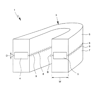
In a highly schematic, perspective view, Fig. 1 shows a proposed device 1
according to a first
.. embodiment. Fig. 2 shows the device 1 in a schematic side view with
associated field-
generating means 10. Fig. 3 shows the device 1 in a schematic top view without
the field-
generating means 10.
The device 1 is used to guide carriers 2 (indicated schematically in Fig. 2),
each of which has
an electrical charge and/or a magnetic moment. The carriers 2 are particularly
charge carri-
ers, especially preferably electrons. However, they can also be so-called
holes, i.e., electron
holes.
The device 1 has a guide device 3 for movably guiding the carriers 2. The
guide device 3 is
.. particularly a solid body or solid structure. The carriers 2 can thus move
particularly in a solid
body or solid structure.
Preferably, the carriers 2 can move at least substantially only in one -
particularly flat and/or
laminar - movement region B, as indicated in Fig. 2.
The device 1 or guide device 3 is preferably provided with electrical
connections 4 and 5,
which are indicated in Figs. 1 and 3.
CA 02972678 2017-06-29
- 8 -
In the depicted example, the device 1 or guide device 3 is preferably
constructed from a first
solid body or semiconductor 6 and a second solid body or semiconductor 7.
These are ar-
ranged over one another in laminar fashion and/or have a common boundary
surface 8.
The contact or boundary surface 8 of the two solid bodies or semiconductors 6,
7 or move-
ment region B is preferably at least substantially flat and/or extends
preferably at least sub-
stantially along a closed - particularly flat or spherical - surface and/or in
a plane E, as indi-
cated in Fig. 2.
The layers or solid bodies 6, 7, lying on top of each other, preferably form a
two-dimensional
electron gas for the carriers 2. In the terms of solid-state physics, the
electron gas consists of
freely movable carriers 2 in the form of electrons or holes in the conduction
band, particularly
with a large mean free path length of preferably greater than 100 nm,
particularly greater
than 200 nm. This especially conductive zone is preferably formed only on both
sides of the
boundary surface 8, i.e., in the form of a very thin layer that forms the
movement space B for
the carriers 2.
As mentioned previously, instead of electrons, these can be, for example, so-
called holes i.e.,
electron holes, that can move as charge carriers at least largely freely and
particularly with a
large mean free path length in the movement region B.
The guide device 3 and/or the movement region B preferably forms a curved or
angled main
path H for the carriers 2, with several parallel main paths H being indicated
schematically in
Fig. 3.
The guide device 3 and/or the movement region B and/or the main path H is
preferably
curved in an arcuate manner, particularly in semicircular or horseshoe-shaped
fashion. Alter-
natively or in addition, however, the guide device 3 and/or the movement
region B and/or the
main path H can also be angled a single time or multiple times.
Especially preferably, the guide device 3 and/or the movement region B and/or
the main path
H extends at least substantially in a surface or plane E, very especially
preferably here the
CA 02972678 2017-06-29
- 9 -
plane E of the boundary surface 8, and is curved and/or angled in this surface
or plane E. This
is conducive to very easy execution and manufacture, particularly in terms of
the application
of very thin layers having a defined thickness.
The connections 4 and 5 are preferably arrangedand/or spaced apart from one
another along
the main path H, particularly in the area of the ends of the arch or angling
of the guide device
3 or movement region B.
The movement region B is preferably layer-like and/or multilayered. The
movement region B
or the respective layer preferably has a mean thickness D of less than 500 nm,
particularly
less than 300 nm, especially preferably about 200 nm or less.
The mean width W of the movement region B and the radius of curvature R of the
main path El
corresponds or correspond at least substantially to the mean free path length
of the carriers 2
in the movement region B or is or are preferably smaller.
The (mean) radius of curvature R of the guide device 3 and/or of the movement
region B
and/or main path El is preferably greater than 100 nm, particularly greater
than 200 nm,
and/or less than 2000 nm, particularly less than 1600 nm.
The mean width W of the movement region B is preferably greater than 80 nm,
particularly
greater than 100 nm, and/or less than the (mean) radius of curvature R.
The boundary surfaces of the movement region B are preferably embodied such
that the car-
riers 2 are reflected; in principle, this can occur specularly (i.e., the
angle of reflection corre-
sponds at least substantially to the angle of incidence) or non-specularly,
i.e., in a particularly
diffusely scattering manner.
Especially preferably, the carriers 2 are reflected particularly on lateral
flanks 9 of the move-
.. ment region B. This preferably occurs in a diffusely scattering and/or at
least partially non-
specular manner.
CA 02972678 2017-06-29
The device 1 preferably has the field-generating means 10. Alternatively, this
field-generating
means 10 or the field F generated by it can be only associated with the device
1 and/or act on-
ly on the device 1 or guide device 3 or movement region B.
5
The field-generating means 10 is used to generate or control a field F for
guiding the carriers 2
at least substantially along the main path H, particularly so that a different
probability densi-
ty/presence density of the carriers 2 is or can be generated at the
connections 4 and 5 and/or
in the vicinity of the ends of the arcuate or angled main path H.
to
The field F is indicated schematically in Figs. 2 and 3.
The field F is particularly a magnetic field. The field-generating means 10 is
thus designed par-
ticularly to generate a magnetic field. As a matter of principle, permanent
magnets can be
used for this purpose. Alternatively, however, electromagnets can also be
used, particularly in
order to generate an electromagnetic field as a field F for guiding the
carriers 2.
Preferably, the field-generating means 10 is embodied such that the field F
for guiding the car-
riers 2 acts at least substantially only in the area of the curvature or
bending of the movement
region B and/or guide device 3 and/or deflects the carriers 2 onto curved
paths at least sub-
stantially only in that area.
The field F for guiding the carriers 2 and/or the field-generating means 10 is
or can be prefer-
ably set up or adapted or even controlled or regulated such that the carriers
2, starting from a
mean speed - particularly as a function of the mean kinetic energy or thermal
energy - are
guided through the field F (particularly due to the Lorentz force with a
gyroradius Z, as indi-
cated schematically in Fig. 3) at least substantially along the curved or
angled main path H
and/or at least substantially with the mean radius of curvature R in the guide
device 3 or in
the movement region B. As mentioned previously, this applies particularly only
to a direction
of motion along the main path H and not in the opposite direction. This
asymmetry is im-
portant with respect to the proposed non-uniform distribution of the carriers
2 in the move-
ment region B or along the main path H.
CA 02972678 2017-06-29
- 11 -
The gyroradius Z effected by the field-generating means 10and/or by the field
F is preferably
on the order of magnitude of the (mean) radius of curvature R of the guide
device 3 or of the
movement region B. Especially preferably, the gyroradius Z is smaller or
greater than the ra-
dius of curvature R by no more than a factor of 5, especially preferably by no
more than a fac-
tor of 2. In particular, the gyroradius Z corresponds at least substantially
to the radius of cur-
vature R.
Due to the different probabilities of presence of the carriers 2 in the area
of the ends of the
angled or curved main path H, an electrical voltage, particularly also an
electric current and
hence also electrical power, can be emitted or tapped via the connections 4
and 5 arranged
particularly in these areas.
In the depicted example, the connections 4 and 5 are arranged particularly on
the two front
sides or ends of the movement region B and/or main path H and/or the guide
device 3.
As required, several guide devices 3 or movement regions B can also be
arranged with their
flat sides on top of one another. These are then preferably penetrated by the
same field F. In
particular, these can be optionally connected in parallel or serially,
particularly to the connec-
tions 4 and 5 or other connections.
The proposed device 1 can be used particularly to generate an electrical
voltage or power
from the thermal or heat energy of charge carriers 2 and/or from the
electromagnetic inher-
ent or ambient noise and/or from electromagnetic influence or radiation by
tapping the volt-
age or power via the connections 4 and 5. The field F is preferably maintained
at least sub-
stantially constant. Alternatively, however, the field F can also be
controlled or regulated in
order to achieve or exceed a defined value or reach a maximum in the tapped
current or pow-
er.
Alternatively or in addition, the proposed device 1 can also be used for
cooling through the
removal of thermal or heat energy from the carriers 2 by tapping electrical
power via the con-
nections 4 and 5. It is thus also possible to cool the device 1 itself. This
can also be conducive
to taking power, which constitutes a self-reinforcing effect.
CA 02972678 2017-06-29
- 12
During cooling, the field F is preferably maintained at least substantially
constant. Alternative-
ly, however, the field F can also be controlled or regulated in order to
achieve or exceed a de-
fined value or reach a maximum in the tapped voltage or power.
Furthermore, it is possible to use the proposed device 1 for measuring or
determining scatter-
ing or trajectories of charge carriers 2 by measuring the electrical voltage
via the connections
4 and 5. In particular, the acting field F can be varied, thereby inferring
corresponding scatter-
ing or trajectories of charge carriers 2 by identifying maxima in the measured
electrical volt-
age, for example.
In general, the proposed principle can also be used to measure or determine
physical charac-
teristics within a one- or two-dimensional electron gas or superconductor if
the movement
region B is formed in or by such a one- or two-dimensional electron gas or
superconductor.
Accordingly, the voltage present at corresponding connections 4 and 5 provides
information
about the physical characteristics, particularly as a function of the acting
field F or magnetic
field.
The proposed principle can also be used to measure or identify magnetic field
strengths or
other fields F acting on the guide device 3 by measuring the electrical
voltage via the connec-
tions 4 and 5. Namely, this depends on the acting field F, as will be
explained in further detail
later on in relation to the third embodiment and the related diagram. In
particular, with prop-
er calibration, the acting magnetic field strength of the field F can be
determined from the
measured electrical voltage.
Additional embodiments of the proposed device 1 of the present invention are
explained in
further detail with reference to the other figures. The preceding remarks,
aspects, and fea-
tures apply particularly in analogous or supplementary fashion even if a
repeated description
is omitted.
In a schematic view corresponding to Fig. 1, Fig. 4 shows a proposed device 1
according to a
second embodiment.
CA 02972678 2017-06-29
- 13
The second embodiment differs from the first embodiment only in that, instead
of an electron
gas, a thin superconducting layer 11 is preferably used to form the movement
region B. The
superconducting layer 11 is preferably formed or arranged by or on the solid
body 6 or 7
and/or particularly between the two, as is indicated in Fig. 4.
The dimensioning of the layer 11 or of the movement region B formed by it
preferably corre-
sponds to the movement region B described in relation to the first embodiment
and the di-
mensioning thereof, so that reference is made thereto.
The carriers 2 are particularly present in the superconducting layer 11 as
electrons or holes,
i.e., electron holes.
A superconducting material of so-called type II is particularly used for the
layer 11, so that, in
.. the case of higher magnetic fields, magnetic field lines in the form of so-
called flux lines or vor-
tices penetrate into the material, with so-called hard superconducting
materials being prefer-
ably used in which the flux lines are held up to a defined threshold force
that is as high as pos-
sible so that they have a high flux-flow resistance.
.. In a schematic top view, Fig. 5 shows a proposed device 1 according to a
third embodiment.
This is a schematic representation of an implemented experimental setup.
A layer 6 is applied to a lower layer or a lower substrate or solid body 7 the
layer 6 particular-
ly forming a layer system or layer package or is constructed as such.
Especially preferably, the layer 6 or layer system is constructed according to
the experimental
setup as follows:
A layer of a first semiconductor material, particularly GaAs, and a layer of a
second semicon-
ductor material, particularly A10.33Ga067As, are layered over one another. In
particular, these
CA 02972678 2017-06-29
- 14 -
layers are layered multiply over one another in an alternating manner,
preferably more than
or 20 times, particularly between 20 and 100 times, and in the experimental
setup espe-
cially preferably 50 times. A layer package is thus formed.
5 The thickness D of the individual layers is preferably less than 50 nm,
particularly less than 25
nm, especially preferably less than 10 nm, and most preferably about 5 nm.
The layer package is optional and is preferably arranged on a base layer or
intermediate layer,
particularly of GaAs and/or with a thickness of greater than 100 nm,
especially preferably
10 greater than 250 nm, most preferably with a thickness of about 500 nm.
A covering layer or first layer of preferably greater than 500 nm,
particularly greater than 750
nm, especially preferably about 1000 nm, and/or preferably of GaAs is
preferably applied to
the layer package or another substrate.
In turn, another or second layer of A10.33Ga0.67As with a thickness of about
10 to 50 nm, espe-
cially preferably about 35 nm, is preferably applied to this GaAs layer.
Preferably, yet another
layer or first covering layer, particularly of A10.33Ga0.67As, particularly
with silicon doping of
preferably 1.5 = 1018 cm-3 and/or with a thickness of preferably greater than
25 nm, particular-
ly about 45 nm, is applied over that.
Subsequently, another layer or covering layer can be applied, particularly of
GaAs, especially
preferably with a thickness of greater than 10 nm, and about 15 nm in the
experimental setup.
The two-dimensional electron gas and laminar movement region B is preferably
formed in the
boundary region between the first layer or 1000 nm layer, here of GaAs, and
the second layer
or 35 nm layer, here of undoped A10.33Ga0.67As.
The aforementioned layer system is especially preferably applied to the lower
layer system or
the lower solid body 7. In the experimental setup, this layer or solid body 7
especially prefer-
ably consists of a semiconducting GaAs substrate.
CA 02972678 2017-06-29
- 15 -
That is, the following layer system was especially preferably used in the
experimental setup:
Name/designation Preferred composition Preferred thickness
Additional covering layer GaAs 15 nm
First covering layer Al033GaØ67As:Si 1.5 = 1018 cm-3 45 nm
Second layer A10.33Gati.67As 35 nm
First layer GaAs 1000 nm
Multiply superimposed thin layers GaAs .. 5 nm
A10.33Ga067As 5 nm
Intermediate layer GaAs 500 nm
Lower layer! substrate S-I GaAs > 500 nm
The layer 6 or layer system thus forms a two-dimensional electron gas and
hence a movement
region in the abovementioned sense, as described in connection with the first
embodiment.
Reference is therefore made to the remarks and explanations regarding the
first embodiment,
which apply analogously or additionally.
In the illustration according to Fig. 5, the surface or plane E of the
movement region B or the
boundary surface 8 lies within the layer system 6 in the drawing plane or
parallel thereto.
CA 02972678 2017-06-29
- 16
In the third embodiment, the guide device 3 and/or layer 6 and/or the layer
system prefera-
bly form two tapering and/or converging legs 12, which form or lead to the
connections 4 and
5.
In particular, the layer 6 or the layer system forms the guide device 3 in the
form of a singly or
multiply, particularly doubly, angled profile. In particular, a substantially
U-shaped profile is
formed in the top view or in the plane of the movement region B or for the
main path H, as in-
dicated in Fig. 5.
The movement region B or the guide device 3 is particularly limited to the
upper U-shaped re-
gion of the layer 6 or the region indicated by the main path H in Fig. 5.
The mean width W of the angled or U-shaped profile or of the movement region B
is prefera-
bly greater than 200 nm, particularly greater than 500 nm, and/or less than
9000 nm, particu-
larly less than 7000 nm.
In the experimental setup, a mean width W of about 600 to 650 nm was obtained.
In the ex-
perimental setup, the interspace in the region of the two connections 4 and 5
was also prefer-
ably as much as the mean width W or less.
The proposed setup or arrangement can be produced in a relatively simple
manner particular-
ly by photolithographic means or through appropriate etching or,
alternatively, through laser
processing or laser ablation.
Preferably, different semiconductor materials are used for the layer system.
In the experimental setup, the abovementioned semiconductor materials in
particular were
used for the layer system 6 and/or mean free path lengths around 600 nm were
achieved.
CA 02972678 2017-06-29
- 17
The field F or magnetic field preferably extends at least substantially
perpendicular to the
drawing plane or plane E (not drawn in), as indicated in Fig. 5.
In the proposed experimental setup, the voltage on the one hand and the
current on the other
hand were measured via the legs 12 or connections 4 and 5 as a function of the
magnetic field
applied or the resulting magnetic flux density. Figs. 6 and 7 show the
resulting diagrams and
curves.
It can clearly be seen from Figs. 6 and 7 that an extreme value, more
particularly a minimum
and maximum, is obtained for the voltage and current, respectively, at about
0.2 T. This is
commensurate with theoretical calculations for the mean radius of curvature R
of about 600
nm implemented here. The measurements were performed at temperatures below 20
K.
The resulting diagrams and measurement curves are - as expected - symmetrical
to the zero
point of the magnetic field (more precisely of the magnetic flux density) and
can be explained
by the fact that, given the magnetic flux density of about 0.2 T under the
stated test conditions,
the charge carriers are guided at least substantially along the main path H,
that is, within the
desired movement region B and/or guide device 3, namely in dependence on the
direction of
the magnetic field once in one direction and once in the other direction, so
that opposite po-
larities are obtained at about +0.2 T and -0.2T for the voltage and the
current, respectively.
Alternatively or in addition, the offset that can be seen as original
measurement data in the di-
agrams according to Figs. 6 and 7 can be explained by electrostatic or Peltier
effect-related in-
terference, which is, however, independent from (invariant to) the magnetic
field.
Fig. 8 shows a current/voltage characteristic measured using the described
experimental set-
up or device 1 tapped externally. This characteristic shows that electrical
power can be gener-
ated and/or be emitted and/or tapped from the proposed device 1.
Accordingly, an electrical voltage or electrical power can thus be tapped by
means of the pro-
posed experimental setup or device 1 and generated or made available from the
thermal en-
ergy of the charge carriers 2 or the device 1 or the guide device 3 and/or
from the electro-
CA 02972678 2017-06-29
- 18 -
,
magnetic inherent or ambient noise or from electromagnetic influence or
radiation. In other
words, it is thus possible to use the device 1 for the provision of electrical
energy or power by
means of an electrical tap via the connections 4 and 5.
Alternatively or in addition, it is also possible to use the device 1 for
cooling. To wit, if electri-
cal power is tapped via the connections 4, 5, thermal energy is drawn from the
charge carriers
2 or the device 1 or guide device 3, whereby a cooling effect or temperature
reduction can be
achieved.
Especially preferably, the field-generating means 10 or the field F for
guiding the carriers 2
can be controlled or regulated in order to reach or exceed a defined or
desired level of tapped
electrical voltage or power or in order to reach a maximum of the tapped
electrical voltage or
power.
As mentioned previously, the proposed device 1 or the proposed principle is
universally ap-
plicable.
In particular, the voltage tapped via the connections 4, 5 can also be used to
measure or de-
termine other characteristics, particularly the measurement or determination
of scattering or
trajectories of charge carriers 2 with appropriate calibration or appropriate
variation of the
respective conditions, such as the field F.
Furthermore, it is also possible to measure or determine physical
characteristics of the guide
device 3 and/or of the movement region B and/or of the carriers 2 movable
therein through
the measurement and analysis of the electrical voltage tapped via the
connections 4, 5. This is
especially the case if a one- or two-dimensional electron gas or a
superconductor is used as a
guide device 3 or for the movement region B or as a (conductive) layer 11.
Moreover, the proposed device 1 - without, however, the field-generating means
10 - can also
be used to measure magnetic field strengths or magnetic flux densities acting
on the guide de-
vice 3 by measuring the electrical voltage via the connections 4 and 5. Then,
with appropriate
calibration, the acting magnetic flux density is accordingly very easy to
determine and/or
CA 02972678 2017-06-29
- 19 -
identify. The device 1 (without field-generating means 10) can then be
regarded and used par-
ticularly as a magnetic sensor.
Alternatively or in addition, the proposed device 1 can also be used or
employed to detect or
.. measure electromagnetic inherent or ambient noise (of the carriers 2)
and/or an electromag-
netic influence or radiation.
Fig. 9 shows the result of current measurements that were carried out on an
experimental
setup in terms of the invention and tapped or measured via the connections 4
and 5. It
demonstrates how robust the effect of unequal conductivity is in the two
directions that are
dependent on the orientation of the magnetic field. In this experiment, an
additional alternat-
ing current voltage coming from the outside was applied to the setup in order
to provide exci-
tation in the MHz range, and this applied voltage was varied over a wide range
from 0 to about
1 V.
The measurement was performed at about 10 K.
With a measurement series B = 0 T, the neutral curve was defined which shows
the current
without an external magnetic field but under inclusion of all other possible
sources of inter-
ference (such as currents as a result of electrochemical contacts or
thermoelectric voltages).
The measurement series with the magnetic field B = + 0.15 T shows that the
preference for
conductivity in the positive current direction remains positive over all
excitation frequencies
and the resulting current is approximately proportional to the alternating
current voltage ap-
plied. The measurement series with the magnetic field B = - 0.25 T shows, in
addition, that the
preference for conductivity in the negative current direction remains negative
over all excita-
tion frequencies and the resulting current is also approximately proportional
to the alternat-
ing current voltage applied. In particular, however, it should be emphasized
that even in the
complete absence of an external excitation (i.e., where V = 0), a positive (B
= + 0.15 T) or nega-
tive (B = - 0.25 T) current flows in departure from the case without a
magnetic field (see in-
.. sect or enlargement in Fig. 9). This is proof that continuous electrical
output can be tapped ex-
ternally from the setup or device 1 according to the invention that does not
originate from the
influence of other possible sources of interference (such as currents
resulting from electro-
chemical contacts or thermoelectric voltages), but rather only from the
thermal energy of the
electrons or the inherent or ambient noise.
CA 02972678 2017-06-29
- 20 -
In a schematic representation corresponding to Fig. 1, Fig. 10 shows a fifth
embodiment of the
proposed device 1 with several movement regions B or electron gases that are
particularly
layered with their flat sides on top of one another.
The several movement regions B are preferably formed in or by a common guide
device 3.
The several movement regions B are preferably connected in parallel and/or
connected via
common electrodes 4, .5.
Different intermediate or depletion layers can be arranged or formed between
the various
movement regions B or electron gases as needed.
The foregoing remarks apply particularly in an analogous or supplementary
manner to the
fifth embodiment just as they do to the previous embodiments, for which reason
repetitions in
this regard will be omitted.
In general, it should be noted that, by means of the present invention, more
precisely the de-
vice 1 according to the invention and the method according to the invention,
an asymmetrical
or direction-dependent conductivity can be or is generated and, accordingly,
an electrical cur-
rent, an electrical voltage, and/or an electrical power can be tapped or made
available. In par-
ticular, a conversion of kinetic or thermal energy into electrical energy is
made possible in a
simple and efficient and/or direct manner.
As mentioned previously, individual aspects and features of the present
invention and its var-
ious embodiments can be implemented individually and combined with one another
as de-
sired.
CA 02972678 2017-06-29
- 21
List of reference symbols:
1 device
2 carrier
3 guide device
4 connection
5 connection
6 layer / solid body
7 layer / solid body
.. 8 boundary surface
9 flank
10 field-generating means
11 superconducting layer
12 leg
B movement region
E plane
F field
H main path
R radius of curvature
Z gyroradius of the carriers