Note: Descriptions are shown in the official language in which they were submitted.
DEVELOPMENT PLATFORM FOR MULTI-WIRELESS TRANSMISSION CAPABILITIES
REFERENCE TO RELATED APPLICATION
[0001] The application is a formal application based on and claiming the
benefit of US
Provisional Application No. 62/360,653 filed July 11, 2016, and hereby
incorporated by reference.
FIELD OF THE DISCLOSURE
[0002] The disclosure is generally directed at product development, and
more specifically
at a method and apparatus for product development.
BACKGROUND OF THE DISCLOSURE
[0003] Many companies are trying to explore markets with new wireless
products or by
adding wireless connectivity to their existing products. Some of these
companies develop the
need to build customized hardware that meet specific requirements depending on
the application.
Additional to the typical challenges of building customized hardware, are the
challenges of
selecting an application-appropriate wireless technology, integrating wireless
components into
the design, and maintaining or improving device performance while minimizing
cost, size and a
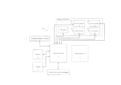
degradation in user experience.
[0004] Successful wireless hardware design requires a strong
understanding of the
product use case requirements, especially pertaining to the wireless
requirements, i.e. how much
data to be wirelessly transmitted/received, how often will data be exchanged,
what physical
distance will the data need to travel over the air, what environmental factors
will affect the
transmission properties, how many devices are part of the wireless network,
how long is each
device expected to be powered, will expenses be incurred by data traffic over
the network, etc.
Some systems that collect and process data can require that different types of
end-devices be
communicated with, each with their own individualized system requirements.
Existing solutions
are restricted to limited performance metrics or removal of certain use cases
altogether.
[0005] Further challenges can arise in the design phase as the number of
available
wireless technologies has grown substantially over the last several years,
which gives a lot of
flexibility from a design standpoint, but a lot of confusion in terms of which
technology is the most
suitable. On top of the wireless system requirements, additional factors such
as world region,
device count, and data costs can play into this decision. Designs with
requirements that cross
multiple of these avenues will require multiple skews of hardware for even a
single frequency
1
CA 2972719 2017-07-10
wireless transceiver solution. Thus, creating the requirement of a system that
uses multiple
coexisting wireless networks that can span different frequency domains and
physical ranges.
[0006] In the development phase of the design, additional challenges
arise of integrating
wireless components into a new or existing design. Development of system
software and
application level design can only fully begin once the hardware has been
qualified, which could
take multiple board design revisions, and a variable number of resources,
including design tools,
designers and test equipment. As a product development cycle, the additional
time required to
overcome these challenges, increases the barrier to entry for solutions that
require custom
designs in a short period of time.
[0007] When data is collected from multiple end-devices, processing
usually occurs, and
with the thought of limiting the amount of data to be transferred to a cloud
network, it can be
favourable to process data in the local network prior to transferring the
data. In a non-deterministic
environment, the end-device data being transmitted can be changing and non-
typical in many
scenarios. Few devices can manage and handle this data traffic efficiently,
with a constantly
changing and updating environment.
[0008] Therefore, there is provided a novel method and apparatus for a
development
platform.
SUMMARY OF THE DISCLOSURE
[0009] The disclosure is directed at a method and apparatus for product
development.
Many companies are trying to enter markets with new wireless products or by
adding wireless
connectivity to their existing products. Some of these companies develop the
need to build
customized hardware that meets specific requirements depending on the
application. The system
and method of the disclosure provides quicker hardware development cycles to
create
opportunities to bring products to market faster.
[0010] In one aspect of the disclosure, there is provided an apparatus
for accelerating
product development including a central processing unit; a wireless
connectivity subsystem
including a set of at least two transceivers for communicating wirelessly with
external devices;
and an external connectivity subsystem including a set of ports for enabling
wired communication
with the central processing unit.
[0011] In another aspect, the set of at least two transceivers are
selected from a group
including a GNSS receiver, a cellular LTE modem, a LoRa transceiver, a BT/WLAN
transceiver
and a Sub-1GHz transceiver. In a further aspect, the system further includes a
memory
subsystem whereby the includes at least one of flash memory, RAM memory or an
external
2
CA 2972719 2017-07-10
microSD connector. In another aspect, the system includes a sensor subsystem
whereby the
sensor subsystem may include at least one of a movement sensor chip and a
temperature sensor.
In a further aspect, the movement sensor chip includes an accelerometer and a
gyroscope.
[0012] In a second aspect of the disclosure, there is provided a method
of code
development for a proposed product including receiving a set of requirements
for the proposed
product; retrieving and displaying a set of hardware subsystems for the
proposed product based
=on the set of requirements for the proposed product; receiving a set of
development code for
execution on the set of hardware subsystems; performing a simulation by
executing the
development code on the set of hardware subsystems; and displaying results of
simulation.
[0013] In a third aspect of the disclosure, there is provided a system
for development of
code including a set of code development platform apparatus, each of the set
of code
development platform apparatus including a central processing unit; a wireless
connectivity
subsystem including a set of at least two transceivers for communicating
wirelessly with external
devices; and an external connectivity subsystem including a set of ports for
enabling wired
communication with the central processing unit; wherein one of the set of code
development
platform apparatus is seen as a back-end apparatus and the rest of the set of
code development
platform apparatus are seen as front-end apparatus; whereby the back-end
apparatus
communicates simultaneously with the front-end apparatus via the wireless
connectivity
subsystem to transmit information concerning development code simulations.
[0014] In another aspect, each of the front-end apparatus backhaul data
to the back-end
apparatus for analysis. In a further aspect, the back-end apparatus uses
artificial intelligence or
machine learning for the analysis. In yet a further aspect, one of the front-
end apparatus receives
and analyzes data and transmits the data and analysis to the other of the set
of core development
platform apparatus whereby the analysis may be performed using artificial
intelligence or machine
learning. In an aspect, the analysis is performed in a local configuration
without Internet
connectivity.
BRIEF DESCRIPTION OF THE DRAWINGS
[0015] Embodiments of the present disclosure will now be described, by
way of example
only, with reference to the attached Figures.
[0016] Figure 1 is a perspective view of an apparatus for product
development;
[0017] Figure 2 is a schematic diagram of an apparatus for product
development;
[0018] Figure 3 is a more detailed schematic diagram of an apparatus for
product
development;
3
CA 2972719 2017-07-10
[0019] Figure 4 is a flowchart outlining a method of product development;
[0020] Figure 5 is a flowchart outlining a method of product development;
and
[0021] Figures 6a to 6c are schematic diagrams of a network of apparatus
for product
development.
DETAILED DESCRIPTION OF THE DISCLOSURE
[0022] The disclosure is directed at a method and apparatus for multi-
wireless channel
communication or transmission. In one embodiment, the apparatus includes a
wireless structure
having a development platform that incorporates a computing platform, wireless
radios, sensors
and interfaces. The apparatus includes at least two different wireless radios,
or transceivers, for
communicating with other external devices.
[0023] Turning to Figure 1, a perspective view of apparatus for
simultaneous multi-
channel wireless communication, or a development platform, is shown. The
apparatus 100
includes a housing 102 which houses the components for enabling the multi-
channel wireless
communication or transmission. The apparatus 100 further includes a set of
ports 104 for
receiving cables connecting the apparatus to other external devices. In the
current embodiment,
the set of ports 104 include a micro-USB port 106, a port for both a nano-SIM
card or microSD
card 108, a USB port 110, a port for a parallel interface camera 112, a high-
definition multimedia
interface (HDMI) port 114 and an external power connector 116. It will be
understood that other
types of ports are contemplated and that different arrangements and/or
combination of ports are
also possible and are not restricted to the set of ports 104 as schematically
shown in Figure 1.
[0024] Turning to Figure 2, a schematic diagram of apparatus for
simultaneous multi-
channel wireless communication is shown. In other words, Figure 2 is directed
at one
embodiment of components integrated or stored within the housing of Figure 1.
In a preferred
embodiment, the apparatus can be used for accelerating a product development
process. This
will be described in more detail below.
[0025] The apparatus 100 includes a processor, such as a central
processing unit (CPU)
200 that is powered by a power subsystem 202. In a preferred embodiment, the
processor 200
is a performance-based applications processor with an ARM Cortex A7 core to
support
algorithm and data processing. In preferred embodiments, various interfaces or
protocols are
used for communication between the processor 200 and the different components
of the
apparatus 100. Some examples include, but are not limited to, secure digital
input output (SDIO),
double data rate 3 low voltage synchronous dynamic random access memory (DDR3L
SDRAM),
quad serial peripheral interface (QSPI), 24-bit Parallel LCD, 8-bit Parallel
Camera, universal
4
CA 2972719 2017-07-10
asynchronous receiver/transmitter (UART), inter-integrated circuit (I2C),
serial peripheral interface
(SPI), controller area network bus (CANBUS), inter-IC Sound (I2S),
Sony/Philips digital interface
format (S/PDIF), USB2.0, joint tag action group (JTAG) and general-purpose
input/output (GP10)
interfaces. The processor 200 supports power management features which
include, but are not
limited to, dynamic voltage frequency scaling (DVFS), clock gating, power
islands, on-board
power regulation and low power modes. The low power mode is preferably
configured to achieve
low or minimal power consumption, which in turn, reduces the overall
temperature of the system.
In one embodiment, the processor 200 has an integrated floating-point unit to
accelerate floating
point operations performed by the processing algorithm.
[0026] The processor 200 is also connected to apparatus for external
connectivity 204
which include, or is associated with, the set of ports 104. The apparatus for
external connectivity
204 may be used to allow wired communication between the apparatus 100 and
external devices,
such as, but not limited to, USB peripherals 362 (cameras, etc.), external
displays 352, audio
devices 360, and CAN bus network devices 358. A plurality of sensors 206 are
also connected
to the CPU 200 and provide various information such as, but not limited to,
external conditions
surrounding the apparatus, orientation of the apparatus, or stabilization.
Memory 208 for storing
data is also located within the housing 102. The system 100 further includes a
set of
buttons/switches 210 which may be used to assist in controlling or resetting
the apparatus 100.
[0027] As shown in Figure 2, the system further includes a wireless
connectivity section,
or apparatus 212 for enabling simultaneous multi-channel wireless
communication between the
apparatus 100 and other devices. The wireless connectivity section 212
includes a set of at least
two different transceivers allowing the apparatus 100 to communicate with
multiple external
parties over different communication channels at the same time. In the current
embodiment, the
wireless connectivity section 212 includes a global navigation satellite
system (GNSS) receiver
214, a cellular LTE modem 216, a long-range (LoRa) transceiver 218, a
BluetoothTmM/iFiTm
(BT/WiFi) transceiver 220 and a sub-1GHz transceiver 222 although transceivers
and other
combination of transceivers are contemplated. Each of the transceivers 214 to
222 is individually
connected to the CPU 200 such that the processor can independently communicate
via the
transceivers with the external devices or entities at the same time.
[0028] In one embodiment of operation, the integrated GNSS receiver 214
or GNSS
receiver module functions to obtain a location fix for the apparatus 100. The
receiver 214 includes
an integrated antenna, filtering and matching circuitry as will be understood.
In a preferred
embodiment, the receiver 214 obtains the location fix based on multiple
satellite constellations
including, but not limited to, a Global Positioning System (GPS), a Global
Navigation Satellite
CA 2972719 2017-07-10
System (GLONASS), a satellite-based augmentation system (SBAS), and a Quasi-
Zenith
Satellite System (QZSS). The receiver 214 relies on UART communication to
transfer incoming
data to the CPU 200. In one embodiment, the receiver 214 operates in the
1575.42MHz band. In
order to reduce power consumption when the device location update is not
necessary, the GNSS
receiver 214 may be put into one of the low power tracking modes. The receiver
214 can also be
set on a cyclic tracking frequency for short period wake-ups or set to an
on/off mode for longer
periods of low power operation.
[0029] In one mode of operation, the cellular LTE modem 216 or cellular
radio is used to
transmit data from the apparatus 100 to a wireless wide area network (WAN)
infrastructure that
may, for instance, store the data in the cloud to be retrieved by another
device. In a preferred
embodiment, the cellular LTE modem 216 has the functionality to download data
from the
network, including, but not limited to, OTA (Over-The-Air) software upgrades.
The modem 216
may also include an externally accessible nano-SIM card slot. The cellular
radio 216 preferably
operates in the frequency bands that are allocated for LTE, 3G and 2G cellular
networks which
are typically within the range of 700MHz to 2600MHz.
[0030] In one embodiment, the apparatus 100 may include multiple LTE
modems 216.
As such, the different cellular modems 216 may be selected to provide
different functional
capabilities. These include low data rate LTE categories including, but not
limited to, LTE Cat 1,
=LTE Cat Ml, NB-I0T, etc. Also, in some embodiments, the multiple modems 216
may cover
different frequency bands based on geographical regions, such as North America
and Europe. In
one embodiment, the modem 216 includes an integrated crystal oscillator,
voltage regulator,
matching circuitry, filtering and antenna. Communication between the modem 216
and the
processor 200 is preferably via UART or USB2.0 communication lines.
[0031] In one embodiment of operation, the integrated LoRa transceiver
218 or
transceiver module operates in the 915MHz with low data rates for extended
transmission
distance. The transceiver 218 preferably has an integrated microcontroller,
crystal, memory, radio
transceiver, analog front-end circuitry and matching network as will be
understood. The CPU 200
communicates with the LoRa module 218 via a standard UART interface.
[0032] In one mode of operation, the integrated Bluetooth/WLAN or WiFi
combination
module 220 operates in the 2.4GHz frequency range for Bluetooth and 2.4GHz and
5.0GHz
ranges for WLAN. In preferred embodiments, the Bluetooth portion, or Bluetooth
radio, of the
module 220 has dual-mode functionality of standard Bluetooth and Bluetooth low
energy up to
version 4.1 which includes BR/EDR (Basic Rate and Enhanced Data Rate). The CPU
200
preferably communicates to the WLAN subsystem via 4-bit SDIO and to the
Bluetooth subsystem
6
CA 2972719 2017-07-10
via 4-wire UART lines. The WLAN subsystem supports 802.11a/b/g/n including
MIMO via two on-
board antennas.
[0033] In one embodiment, the Bluetooth radio is implemented such that
the apparatus
100 transmits and receives data wirelessly to/from another Bluetooth enabled
device for short-
range data transfer, collects MAC address data to store for collection and
tracking, and/or
performs OTA software upgrades. Similarly, the WLAN subsystem has similar
capability in terms
of transferring data to an access point and receiving from one, as well as MAC
address data
collection, and OTA software upgrades.
[0034] In one mode of operation, the integrated Sub-1GHz transceiver 222
operates in
the 915MHz frequency band with low data rates for extended transmission
distance. The
transceiver preferably includes an integrated core processor, such as an ARM
Cortex M3 core
processor, memory, radio transceiver, and peripheral communication interface
modules. The
transceiver 222 may also include the capability to operate in the 2.4GHz
frequency band to
support Bluetooth low energy 4.2 specification, 802.15.4g Zigbee, 6LoWPAN, and
other related
networks. The subsystem design requires external on-board analog front-end
circuitry and
matching network. An on-board antenna is also integrated into the design. The
CPU 200
preferably communicates with the integrated sub-1GHz transceiver 222 via a
standard UART
interface.
[0035] In one example, the GNSS receiver 214 can communicate with GPS
satellites to
obtain location information with respect to the presence of the apparatus
while the cellular LTE
modem 216 transmits or receives data over the Internet.
[0036] An advantage of the current disclosure is that for product testing
purposes, an
increased number of different technologies + frequencies that can cover more
use cases, in terms
of high/low data rates, close/long range communication, high/low power
transmissions to connect
many devices in a network are available within one system. For example, the
system could be
using Bluetooth for short range data collection from end node devices 600 in a
local network,
sending that to other gateways over a long range technology such as Sub-1GHz,
and then
backhauling that data through a gateway 100 to the cloud network 604 via
cellular.
[0037] Turning to Figure 3, a more detailed schematic of apparatus for
multi-channel
wireless communication is shown. In Figure 3, certain of the components of the
apparatus 100
are shown in more detail. The multi-channel wireless communication apparatus
may also be
seen as a development platform.
[0038] In the embodiment of Figure 3, the buttons/switches preferably
include a power
button/switch 300, a Sub-1GHz transceiver reset button 302 and a Sub-1GHz GPIO
304 that are
7
CA 2972719 2017-07-10
connected with the sub-1GHz transceiver 222, a GPIO 306 that is connected to
the CPU 200 and
a reset button 308 that is also connected to the processor 200. The buttons
and switches are
provided internally to the housing but are preferably accessible with the lid
opened.
[0039] In preferred embodiments, the apparatus, or wireless platform,
includes multiple
LEDs to provide indications of functionality of the unit. The message or
indications can be
configurable and be used to indicate examples such as the system being
powered, battery states,
wireless radio transmitting periods, and sensor capturing modes. Each LED has
the required state
definitions time-multiplexed within a set period such that each state can be
identified
simultaneously if each mode happens to be in operation at the same time.
[0040] The power subsystem 202 is preferably connected to an external
power connector
309 for providing the necessary power to operate or charge the apparatus 100.
Within the
subsystem is a set of discrete converters 310 and a set power management
integrated circuit
(PMIC) 312 for controlling the power being supplied to the components of the
apparatus 100 via
the power connector 209. A rechargeable battery 311 is also located within the
power subsystem.
[0041] In one embodiment, the power path includes an input from the
external power
source 309 that charges the internal rechargeable battery 311 that
consequently, powers the
system. The rechargeable battery 311 enables portable usage of the apparatus
100 when an
external power source is not available. In a preferred embodiment, the
apparatus 100 accepts a
5V charging input (seen as the external power source 309) to charge the
battery 311. The
charging or power subsystem 202 steps down the voltage from 5V to an
appropriate voltage level
to charge the battery 311. The charging system preferably has built-in
protection for over-voltage,
over-current and under-voltage. These values are determined by the charging
system and
correlate with the battery specifications. A preferred embodiment uses a
battery 311 that is rated
for industrial environments and extreme operating conditions. The input power
is regulated
through the PMIC 312 to deliver power to the various subsystems and components
within the
apparatus 100 through dedicated voltage rails for higher efficiency power
utilization.
[0042] In the embodiment of Figure 3, the sensors include a motion
tracking sensor 314
including an accelerator and gyroscope combination along with a temperature
sensor 316.
Although only two different sensors are shown, other sensors are contemplated.
[0043] In one embodiment, the motion tracking sensor 314 integrates a 3-
axis
accelerometer and a 3-axis gyroscope such that motion in 6 different axes can
be sensed. The
sensor 314 provides functionality including, but not limited to, step
counting, device movement,
and augmented location tracking. The augmented location tracking functionality
may serve as a
companion device and substitute for the GNSS receiver 214 to track current
location based on a
8
CA 2972719 2017-07-10
previously known location in situations when the GNSS receiver 214 is placed
in low power
tracking modes or shutdown mode or if the receiver 214 is not able to acquire
a signal from
satellites.
[0044] With respect to the integrated ambient temperature sensor 316, the
sensor 316
preferably provides up to 14-bit resolution of accuracy and is designed for
accuracy over a large
temperature range. It also requires very low current to operate and is thus an
asset to the
apparatus in that it has low or minimal impact to battery life and has low
power requirements. The
sensor data can be retrieved or transmitted to the processor 200 via an I20
communication
interface.
[0045] Within the memory section, there is preferably a flash memory 318,
RAM memory
320 and an external microSD connector 322 (associated with the microSD port
108). Use of the
flash memory 318, such as NOR Flash, and the RAM memory 320, such as, for
instance, DDR3L
SDRAM, for storage purposes will be well understood by one skilled in the art.
The external
connector 322 allows an external device or memory card to be plugged into the
apparatus 100.
[0046] In one embodiment, the RAM memory 320 has an approximate 4Gb
storage
capacity and can run at speeds of up to 400MHz and uses a dedicated 16-bit
parallel data
interface with 16-bit addressable storage locations. In another embodiment,
the flash memory
318 has approximately 256Mb of storage capacity and can run at speeds of up to
108MHz in a
single transfer rate mode. It will be understood that other storage capacities
can be used and
that the ones listed in this paragraph are merely suggestions. The
communication interface
between the flash memory 318 and the processor 200 is preferably via a 4-bit
QSPI interface.
[0047] The microSD slot or port 108 accepts various storage sizes for
microSD cards, and
uses a 4-bit SDIO interface to transfer data to and receive data from the
processor 200. In a
preferred embodiment, the microSD stores the software image and loads the
device to start up
the system.
[0048] Turning to the external connectivity/debugging system, in one
embodiment, the
debugging system includes an external GIPO interface connector 324, a parallel
camera
connector 326, a USB2.0 connector 328, a JTAG debug connector 330, a HDMI
connector 332,
an SPDIF audio connector 334 and a CANBUS connector 336. In some cases, the
components
within the external connectivity/debugging system are associated with or
connected to the set of
ports 104.
[0049] In preferred embodiments, the parallel camera connector 326 allows
the apparatus
100 to be connected with an external camera 350. The connector 326 may include
a 24-pin
connector interface to provide external 8-bit parallel interface camera sensor
module. The parallel
9
CA 2972719 2017-07-10
camera connector 326 preferably supports video graphics array (VGA) resolution
cameras (640
x 480) and various data formats including: RGB, YCbCr422, and CCI R656.
[0050] In one embodiment, the HDMI connector 332 can be used to connect
the
apparatus 100 to an external monitor or screen 352 to output data to the
display 352. In a
preferred embodiment, the apparatus 100 is capable of driving a display with
up to \A/XGA
resolution (1366 x 768). Since the output from the processor 200 is in the
format of a 24-bit
parallel interface, the apparatus 100 includes an on-board transmitter
component 354 for
converting this output into standard HDMI protocol or signals before being
transmitted to the
display to drive the external display.
[0051] With the CANBUS connector 336, the system 100 may include a CAN
transceiver
356 between the processor 200 and the CANBUS connector 336. The CANBUS
connector 336
allows an external CAN network device 358 to be connected to the apparatus
100. A CAN
controller module within the processor 200 communicates or operates with the
CAN 2.0B protocol
and sends and receives data to/from the CAN transceiver 356. The transceiver
356 converts the
data from the processor 200 to a differential signal to transmit onto the bus
for other CAN nodes
to receive.
[0052] The SPDIF audio connector 334 may be a generic 4-pin connector
that enables
an external audio device 360 to be connected to the apparatus 100 via a 2-wire
SPDIF
communication interface. Alternatively, or in combination, a further audio
connector may also be
a connector to enable an external audio device to connect to the apparatus
that uses I2S as its
communication protocol. External peripheral devices that can operate as a
master or slave can
be connected to the external connectors to transfer data. The I2S module of
the processor is also
tied into pins on the BT/WLAN module to support audio over the air via
Bluetooth.
[0053] The USB2.0 connector 328 enables external devices including USB
peripherals
362, such as a USB camera to be connected to the apparatus 100. In one
embodiment, the USB
Host (type A) connector 328 allows for the USB peripheral device 362 to
connect to the host
processor 200 to transfer data through the USB2.0 High Speed protocol at up to
speeds of
480Mbps. An additional connector may provide a control access port to an
external device that
uses one of the following communication protocols: I2C, SPI or UART. This may
be enabled via
a USB to UART bridge 364. The GPIO connector 324 may also be used to provide
another layer
of control or input to and from an external device 366. The JTAG connector 330
enables an
external computer device 368 to be connected with the apparatus 100.
[0054] The apparatus of the disclosure further includes a database 380
which stores
information, such as programming requirements, for different hardware
subsystems and the
CA 2972719 2017-07-10
characteristics of the components themselves. In one embodiment, the developer
can enter
information associated with a proposed product and the apparatus selects a
"best set" of
subsystems for the developer to use in developing their product. After
selecting the different
components, the developer can write program code and use the development
platform of the
disclosure to test the code against the selected components. In one
embodiment, the
development platform provides a software coding environment for a developer to
use in
developing code for their product without having to purchase the individual
components.
[0055] Turning to Figure 4, a flowchart outlining a method of product
development is
shown. In this embodiment, the method is with regard to a developer. In one
embodiment, the
product may be an electronic device. The method of Figure 4 is preferably used
to design an
electronic device having both hardware and software. Currently, it is a
relatively long process
between defining a product specification and having a physical device in the
user's hands to test
and further develop.
[0056] A developer or user initially determines or defines the product or
prototype
specification (400) based on a desired list of product features. The product
specification controls
the technical requirements and constraints that define the product. Based on
the product
specification, an overarching system architecture can be defined (402) which
takes into account
the interfacing of components to the processor and the power system to provide
stable and
sufficient power to each of the required peripheral subsystems. Hardware and
related software
component selection (404) can then be performed based on the defined system
architecture.
[0057] After the components are selected, the hardware and the software
is designed
(406). In one embodiment, this may also include printed circuit board (PCB)
design along with
software drivers. After the hardware is designed, hardware verification and
software development
is performed. Once the PCBs are fabricated and populated with components, the
hardware
verification can start as well as any software development on top of the
available drivers (408).
The software is also subsequently developed and tested.
[0058] An advantage of the system is a reduction in time between the
development of the
initial requirements and having physical hardware available to begin software
development is
facilitated. For instance, using the system of the disclosure to add wireless
connectivity to an
existing device, a user could plug their device in via one of the external
connectors or ports, when
they are in the initial requirements/specification/architecture portion of the
design flow and have
hardware and software available to start testing. Currently, user need to
qualify the hardware and
software after being designed from the start which takes a lot more time.
11
CA 2972719 2017-07-10
[0059] After the software has met a sufficient level of maturity, device
testing (410) can
begin. Verification results can then be fed into the next revision of
hardware.
[0060] Identifying compatible components from a feature requirements
standpoint and
interface perspective can be a difficult task for experienced and
inexperienced designers alike.
Selecting these components and integrating them into a single board design is
improved by the
apparatus of the disclosure from the viewpoint of a designer's development
cycle. Having pre-
defined hardware that is configurable through software with the specific
components is an
advantage over how it is currently performed. This is described in more detail
below.
[0061] Turning to Figure 5, another embodiment of a method of product
development is
shown. In this embodiment, the method is performed from the viewpoint of the
apparatus.
[0062] The developer initially plugs their processing or computing
device, such as a laptop
and the like into the development platform via one of the ports 104 within the
device, such as the
micro-USB connector. After connecting with the apparatus 100, the developer
can enter
information relating to the requirements and select features, such as wireless
communication
requirements, that a developer needs for their product or the developer can
enter information
associated with a product they wish to produce. This information relating to
requirements and
features for a proposed product are received by the apparatus (500).
[0063] After receiving this information or input from a user or
developer, the apparatus
100 determines or retrieves hardware subsystems for use in the proposed
product (502). This
list may be retrieved from a look-up table based on the entered information
for selection by the
developer or the developer may enter a list of suggested subsystems which may
be reviewed by
the development platform for things such as, but not limited to, compatibility
with each other.
Alternatively, the apparatus may determine suitable hardware subsystems based
on the input
from the developer.
[0064] After the subsystems are selected, the system stores the selected
subsystems in
memory within the apparatus 504. The developer can then write code for
execution on the
selected components and use the apparatus 100 to test or debug the written
code 506. The
system of the disclosure provides flexibility and multiple technology options
in one integrated
device.
[0065] The development platform provides an improved method of software
code testing
without a developer needing to purchase individual components and externally
connect them, as
the development platform provides a simulation environment for multiple
subsystems
concurrently. The results of the testing or simulation can then be displayed
for the developer to
review 508.
12
CA 2972719 2017-07-10
[0066] The apparatus of the disclosure reduces the number of actions to
produce or arrive
at a finished product. A developer can interact with the apparatus of the
disclosure, which can
also be seen as a development platform, to obtain information allowing for
accelerated
development of a product. In a preferred embodiment, the development platform
is used for
developers looking to develop products requiring wireless communication
functionality. By
providing a developer an apparatus that can execute test or source code
without the need for a
physical prototype of the product being built, allows for parallel development
of both the hardware
and software aspects of the product. The delay for a developer in waiting for
a physical prototype
to be manufactured before being able to test their code is shortened or
reduced.
[0067] An advantage of the disclosure is that different components can be
selected and
tested at one time rather than having to test the written code individually on
different components.
As such, the developer can select multiple similar hardware subsystems for the
simulation
whereby the developer can determine with which hardware subsystems the
developed code is
more or most compatible.
[0068] After the code has been validated or reviewed, further product
manufacture can
be performed by the developer based on the subsystems selected or suggested by
the
development platform.
[0069] One advantage of the disclosure is that the apparatus provides
access to unique
combinations of hardware elements, firmware drivers and application-level
software that allows
users to begin their custom development immediately. This process flow allows
the user to skip
the first board design cycle and start directly with their custom software
application development
and device performance testing through use of the wireless platform. In
parallel, this also allows
the user to be able to determine the necessary changes required to alter the
design towards the
next revision of hardware with additional customized subsystems, components
and mechanicals
for their specific application. The overall timeline of the product
development cycle can be
reduced and thus allow the user to take their product to market sooner and
more cost-effectively.
[0070] The wireless platform can be used as a development platform when
incorporated
in any of the preferred system architectural embodiments as seen in Figures 6a
to 6c. Figure 6a
shows a typical configuration in which the apparatus performs the function of
a gateway, such
that it collects data from connected, either wirelessly or wired, end-nodes
600 (which can be seen
as external devices or other apparatus 100), and then backhauls some, all, or
a processed amount
of data to a cloud environment 604. The data transfer will be performed after
some analysis has
been provided via a Machine Learning/Artificial Intelligence layer. Use of
these layers will be
understood by one skilled in the art. Figure 6b shows another system
architecture embodiment
13
CA 2972719 2017-07-10
that allows end-node devices 600 to pass data through one another in a local
area network to
reach a gateway, seen as the apparatus 100 that may not be within the
transmission range of a
distant end-node device. Once again, the gateway 100 provides the connection
to backhaul data
to the cloud environment 604 to transfer data. Figure 6c shows a system
network in which each
end-node (which can now be seen as the apparatus 100) has the technological
capability to
backhaul data to the cloud 604, thus making each end-node its own gateway 100.
[0071] As such, the apparatus 100 can support Edge or Fog computing. In a
Fog
computing instance, multiple apparatus 100 communicate together utilizing any
number of the
. wireless radios available to gather data, backhaul to a single device that
will analyze data locally.
In an edge computing instance, a plurality of apparatus 100 are placed in a
mesh network scenario
such that data received in the network of apparatus can be used as an input
and analysis made
(using Al/ML) and distributed to each of the other edge devices.
[0072] In one embodiment, the apparatus can backhaul data in different
ways. For
instance, for an apparatus using Thread/Zigbee, the sub-1GHz radio or the BT
transceiver, data
processing can be performed by the apparatus and then the data pushed to the
cloud via a high
bandwidth cellular modem. In another embodiment, to an existing internet
connected device, the
data processing can be performed in the cloud environment. In another
embodiment, to the cloud
using a lower bandwidth cellular radio or LoRa, the data processing can be
done by the cloud
environment.
[0073] In another embodiment, the apparatus operates locally without
Internet
connectivity. In this manner, one or more apparatus 100 in different
configurations is/are able to
control end point (or edge) apparatus in the local network by processing their
input data, analyzing
it with artificial intelligence and/or machine learning and making a decision
on how to
deterministrically change the network parameters to better suit the network's
needs.
[0074] As a development tool, the apparatus can be configured as a subset
of integrated
subsystems in order to provide the development environment of a device with
backhaul capability
or as a device with local area network wireless transmission capabilities.
[0075] A preferred embodiment of the disclosure, or wireless platform,
provides a low
power microcontroller capable of, but not limited to, communicating with the
data collection sensor
components to extract data at a specified frequency to upload into a memory
storage location.
The microcontroller uses multiple interfaces to communicate with the
peripheral components, that
include, but are not limited to, UART, I20, SRI, and GPIOs. The
microcontroller implements a
specific schedule to place components into low power modes when not active to
reduce the power
consumption. The low power modes are used frequently to ensure that minimal
power
14
CA 2972719 2017-07-10
consumption is achieved, which in turn, reduces the overall temperature of the
board and internal
device temperature.
[0076] Fog computing can be perceived both in large cloud systems and big
data structures, making reference to the growing difficulties in accessing
information objectively.
This results in a lack of quality of the obtained content. The effects of fog
computing on cloud
computing and big data systems may vary; yet, a common aspect that can be
extracted is a
limitation in accurate content distribution, an issue that has been tackled
with the creation of
metrics that attempt to improve accuracy.
[0077] Fog networking includes a control plane and a data plane. For
example, on the
data plane, fog computing enables computing services to reside at the edge of
the network as
opposed to servers in a data-center. Compared to cloud computing, fog
computing emphasizes
proximity to end-users and client objectives, dense geographical distribution
and local resource
pooling, latency reduction and backbone bandwidth savings to achieve better
quality of
service (QoS) and edge analytics/stream mining, resulting in superior or
improved user-
experience and redundancy in case of failure.
[0078] Edge computing pushes applications, data and computing power
(services) away
from centralized points to the logical extremes of a network. Edge computing
replicates fragments
of information across distributed networks of web servers, which may spread
over a vast area. As
a topological paradigm, edge computing is also referred to as mesh computing,
peer-to-peer
computing, autonomic (self-healing) computing, grid computing, and by other
names implying
non-centralized, nodeless availability.
[0079] Although the present disclosure has been illustrated and described
herein with
reference to preferred embodiments and specific examples thereof, it will be
readily apparent to
those of ordinary skill in the art that other embodiments and examples may
perform similar
functions and/or achieve like results. All such equivalent embodiments and
examples are within
the spirit and scope of the present disclosure.
[0080] In the preceding description, for purposes of explanation,
numerous details are set
forth in order to provide a thorough understanding of the embodiments.
However, it will be
apparent to one skilled in the art that these specific details may not be
required. In other instances,
well-known structures may be shown in block diagram form in order not to
obscure the
understanding. For example, specific details are not provided as to whether
elements of the
embodiments described herein are implemented as a software routine, hardware
circuit, firmware,
or a combination thereof.
CA 2972719 2017-07-10
[0081]
Embodiments of the disclosure or components thereof can be provided as or
represented as a computer program product stored in a machine-readable medium
(also referred
to as a computer-readable medium, a processor-readable medium, or a computer
usable medium
having a computer-readable program code embodied therein). The machine-
readable medium
can be any suitable tangible, non-transitory medium, including magnetic,
optical, or electrical
storage medium including a diskette, compact disk read only memory (CD-ROM),
memory device
(volatile or non-volatile), or similar storage mechanism. The machine-readable
medium can
contain various sets of instructions, code sequences, configuration
information, or other data,
which, when executed, cause a processor or controller to perform steps in a
method according to
an embodiment of the disclosure. Those of ordinary skill in the art will
appreciate that other
instructions and operations necessary to implement the described
implementations can also be
stored on the machine-readable medium. The instructions stored on the machine-
readable
medium can be executed by a processor, controller or other suitable processing
device, and can
interface with circuitry to perform the described tasks.
16
CA 2972719 2017-07-10