Note: Descriptions are shown in the official language in which they were submitted.
BORON NITRIDE NANOTUBE ENHANCED ELECTRICAL COMPONENTS
[0001]
[0002]
FIELD
[0003] The present disclosure generally relates to enhancing the
performance of electrical
components through the inclusion of boron nitride nanotubes.
BACKGROUND
[0004] As electronic and electrical components (ECs), such as diodes, light
emitting diodes
(LEDs), transistors, integrated circuits and multilayer integrated circuits,
become more prevalent
devices, EC performance becomes more critical. In most instances, EC
performance is frequently
limited by the EC's ability to minimize heat production and improver heat
transport away from the
heat generating regions to heat sinks, thereby keeping the junction
temperatures and component
temperatures low and diminishing thermally-generated mechanical stresses in
the materials and
layers making up the EC.
[0005] The diodes, transistors, etc. in ECs all have a certain amount of
electrical resistance.
When electrical currents flow in the ECs, heat is generated. One parameter of
1
Date Recue/Date Received 2022-03-09
CA 02972769 2017-06-29
WO 2016/100715 PCT/US2015/066464
importance is the junction temperature, where one type of semiconductor
interfaces with another
type of semiconductor. This is also the location where much of the resistance
is located. Heat
generated at these locations impacts the performance including lifetime of the
EC. Removing this
heat and keeping the junction temperatures as low as possible is important for
proper functioning
of the EC.
[0006] Carbon nanotubes (CNTs), graphene and pyrolytic graphite can be
incorporated in
ECs where electrically conductive and/or semi conductive properties are
desired. CNTs and
graphene can also favorably affect heat transport and structural strength.
However, they do not
work where the material needs to be electrically insulating. Thus, CNTs have
limited efficacy
with respect to enhancing ECs.
[0007] Boron nitride nanotubes (BNNTs) have been considered for a number
of
prospective applications, such as, for example: enhancing the strength of
ceramic, metal and
polymer composites, functionalizing with other attached molecules for a range
of chemical
reactions, enhancing the thermal conductivity of certain composites, creating
filters and
associated mats, neutron detectors, biomedical interactions including el
ectroporati on for cancer
treatment, piezoelectric devices, and electrically insulating layers in
supercapacitors (also known
as ultracapacitors).
[0008] High quality BNNTs, such as those manufactured by BNNT, LLC of
Newport
News, Virginia, have few defects, no catalyst impurities, 1- to 10-walls with
the peak in the
distribution at 2-walls and rapidly decreasing with larger number of walls.
Although dimensions
may vary depending on the manufacturing process, BNNT diameters typically
range from 1.5 to
6 nm but may extend beyond this range, and lengths typically range from a few
hundreds of nm
to hundreds of microns but may extend beyond this range
2
CA 02972769 2017-06-29
WO 2016/100715 PCT/US2015/066464
[0009] Previous patents and published applications have suggested the
addition of
materials including BNNTs into the materials going into ECs. See for example:
U.S. Patent
Publication US2014/0080954 Al to Raman et al.; and U.S. Patent 6,864,571 B2 to
Arik et al.
However, the methods disclosed Raman merely suggest use of BNNTs in bulk, and
the methods
disclosed by Arik merely suggest "generally aligned nanotubes that extend away
from the
catalyst layer" i.e. in the out-of-plane and similar out-of-plane heat
transfer for limited aspects of
the ECs. Merely dispersing or including the BNNTs into the materials going
into ECs or out-of ¨
plane thermal conductivity is insufficient to enhance the thermal management
in ECs. The
chemical vapor deposition (CVD) growth methods of Arik do not produce high
quality BNNTs,
i.e. few wall, high aspect ratio, minimal defects and catalyst free, as they
take place at
temperatures and nitrogen pressures far below what is required for high
quality BNNTs. Indeed,
Arik's use of chemical vapor deposition to form BNNTs severely limits Arik's
ability to enhance
ECs using BNNT group layers. What is needed are more effective methods for
enhancing
theimal management in ECs.
BRIEF SUMMARY
[0010] This disclosure relates to leveraging the unique properties of BNNTs
by
incorporating them in electronic and electrical components (ECs for both
electronic and
electrical components). The resultant ECs are enhanced by having improved heat
management,
improved dielectric properties, enhanced ionic transport and enhanced
strength. For most of the
incorporation of the BNNTs in electronic and electrical components, the
improved or enhanced
performance includes having BNNTs that are aligned or partially aligned. This
is important as
stated in the Background above because alignment greatly enhances the thermal
conductivity and
further provide desirable dielectric and structural properties. Further, these
properties can be
3
directional; for example the alignment can create thermal direction "pipes"
for transporting the
heat in preferred directions.
[0011] The heat conductivity of groups of BNNTs is greatly enhanced when
the BNNTs are
aligned relative close to each other along their lengths such that phonons can
couple from one
BNNT to another. Also important for enhancing BNNT thermal conductivity is
having very long
BNNTs with few walls and few defects such that phonons have a considerable
length to propagate
and opportunity to couple phonons to other BNNTs or other materials that the
BNNTs have been
composited with or coated with in the case of layered composites. Depending on
the manufacturing
process, high quality BNNTs may have impurities of boron, amorphous BN and h-
BN, all of which
are also electrical insulating materials.
[0012] The pattern of the BNNTs in the materials is important to achieve
optimal performance.
In many instances having directionality of the heat flow is desirable and
BNNTs as described
herein provide this directionality. In other cases uniform heat flow in all
directions is desirable.
The optimum configuration is EC-specific, and thus may vary in different
embodiments. Further,
the electronic properties of the EC, such as the dielectric value, can be
enhanced by the appropriate
alignment of the BNNTs.
[0013] Accordingly, there is described a method for thermal management in
an electrical
component, the method comprising: applying a BNNT group layer to a contact
surface of a
material layer in the electrical component, wherein the BNNT group layer is
aligned generally
parallel to the contact surface such that the BNNTs in the BNNT group layer
are aligned
generally parallel to the contact surface, and wherein at least a portion of
the BNNTs in the
4
Date Recue/Date Received 2022-03-09
BNNT group layer penetrate the contact surface such that the BNNT group layer
is embedded
in the contact surface.
[0013a] In some embodiments, the BNNT group layer may be linearly aligned,
such that the
BNNTs are also generally parallel to each other. It should be appreciated that
"generally parallel"
includes embodiments in which the long axis for the majority of BNNTs in a
BNNT group are
oriented less than 90-degrees relative to the contact surface. In practice,
there are variabilities in
the orientation of BNNTs in a BNNT group. For example, a majority of BNNTs may
be oriented
at less than 90-degrees relative to the surface, a smaller fraction oriented
at less than about 45-
degrees relative to the surface, and an even smaller fraction oriented at less
than about 15-degrees
relative to the surface. Preferably, the long axis for the majority of the
BNNTs are nearly parallel
to the contact surface. In practice, however, BNNTs have non-linear portions,
and thus this
specification references "generally parallel" to account for non-linear
portions as well as the
variability of BNNTs within a BNNT group. The contact surface may include a
source and a drain,
such as in the case of a diode. In some embodiments, the EC may be a
transistor, and the contact
surface may include a source, a gate, and a drain. In some embodiments the
BNNT group layer
may out-of-plan to the layers of the EC such as to provide a layer-to-layer
thermal interconnect.
Of course, an EC such as a transistor or a diode may have other material
layers in contact with a
BNNT group layer. The alignment may be linear, such that the BNNTs are
generally parallel to
each other. Alternatively, the alignment may be two-dimensional or 2-D. The
BNNT group layer
may be, for example, a BNNT mat or a BNNT bundle such as BNNT fibers and woven
BNNT
yarns. ECs may be fabricated to have one or more of these features.
Date Recue/Date Received 2022-03-09
[0014] A variety of techniques may be used to align the BNNT group layer.
For example, the
layer may be aligned through flattening and/or stretching processes. The BNNTs
may also be
aligned in the BNNT synthesis or manufacturing process, as in the formation of
BNNT fibers and
yarns, or as another example in the formation of a BNNT mat.
[0015] In some embodiments, the BNNT group layer may include one or more
compositing
materials. The compositing material(s) may be composited in bulk, e.g.,
generally uniform
throughout the BNNT group layer. In some embodiments, the compositing
material(s) may be site-
specific, e.g., present at specific portions of the BNNT group layer, such as
at certain locations
along the length of a BNNT bundle. Depending on the embodiment, the
compositing material may
be, for instance, a ceramic, a metal, a polymer, an epoxy, and/or a thermal
grease. Some
embodiments may include a compositing material infused in the BNNT group
layer. The BNNT
group layer may be composited with an electrical conductor in some
embodiments. In some
embodiments the BNNT fibers may be first coated with one material and then
that coated BNNT
fibers are composited with a third material.
[0015a] There is also described an electrical component comprising: a material
layer having a
contact surface, and a BNNT group layer in contact with the contact surface;
wherein the BNNT
group layer comprises BNNTs aligned generally parallel to the contact surface,
such that the
BNNTs in the BNNT group layer are aligned generally parallel to the contact
surface, and wherein
at least a portion of the BNNTs in the BNNT group layer penetrate the contact
surface such that
the BNNT group layer is embedded in the contact surface.
[0016] The EC may include a BNNT group layer compressed into the material
layer. Some
ECs, such as integrated circuits, may include multiple layers. In such
embodiments, one or more
6
Date Recue/Date Received 2022-03-09
BNNT group layers may be sandwiched between material layers in the EC. Some
embodiments
may leave terminal ends of the BNNT group layer exposed to the environment,
e.g., such that the
ends of some of the BNNTs may transfer heat directly to the environment (e.g.,
air or another
medium). In some embodiments, the terminal end may be present in a compositing
material, such
that the BNNTs transfer heat to the compositing material.
[0016a] There is further described an electrical component comprising: a
material layer
having a contact surface, and a thermal management BNNT group layer comprising
BNNTs,
the BNNT group layer in contact with the contact surface such that at least a
portion of the
BNNTs have a long axis with an outer surface in contact with the contact
surface; wherein at
least a portion of the BNNTs in the BNNT group layer penetrate the contact
surface, such that
the BNNT group layer is embedded in the contact surface.
DRAWINGS
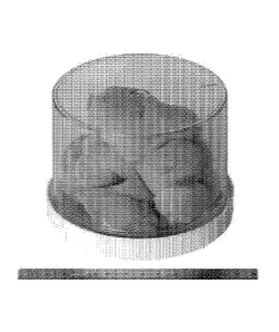
[0017] Fig. 1 shows as produced high quality BNNT material and has the
appearance of a
cotton ball.
[0018] Fig. 2 illustrates how the randomly aligned BNNT molecules or fibers
become aligned
when flattened or stretched.
6a
Date Recue/Date Received 2022-03-09
CA 02972769 2017-06-29
WO 2016/100715 PCT/US2015/066464
[0019] Fig. 3 shows a BNNT cotton ball compressed into a mat thereby
creating
alignment of the BNNT fibers
[0020] Fig. 4 shows BNNT fibers synthesized in one of the high quality
BNNT synthesis
processes where BNNT initial yarns or strands have been created.
[0021] Fig. 5 shows a BNNT mat made from a filtration process.
[0022] Fig. 6 illustrates BNNT yams/strings woven into a BNNT mat.
[0023] Figs. 7A-7C illustrate BNNT fibers, yarns/strings and weaves
composited with
compositing materials.
[0024] Fig. 8 illustrates and end view of in-plane aligned BNNTs between
two layers or
sublayers of an EC.
[0025] Fig. 9 illustrates a side view of in-plane aligned BNNTs between
two layers or
sublayers of an EC.
[0026] Figs. 10A-10C illustrate BNNT bundles with composite interconnects
or heat
sinks for making connections to layers or sublayers of ECs.
[0027] Fig. 11 illustrates a transistor with the aligned BNNTs across the
topside.
[0028] Fig. 12 illustrates multiple transistors with aligned BNNTs across
their topsides.
[0029] Fig. 13 illustrates multi-layered transistors with aligned BNNTs
across the
topsides and, for the lower layer, the bottom side.
[0030] Fig. 14 illustrates multi-layered transistors with aligned BNNTs
across their
topsides and for the intermediate and lower layers their bottom side with the
addition of aligned
BNNTs transporting heat across the multiple layers of transistors.
[0031] Fig. 15 illustrates a light emitting diode where BNNTs can be
utilized to lower its
junction temperature
7
CA 02972769 2017-06-29
WO 2016/100715 PCT/US2015/066464
DESCRIPTION
[0032] The following description is of the best currently contemplated mode
of carrying
out exemplary embodiments of the present approach. The description is not to
be taken in a
limiting sense, and is made merely for the purpose of illustrating the general
principles of the
present approach.
[0033] BNNTs may be present in an EC in a group, e.g., several nanotubes
forming a
layer. The BNNTs in a group may be in various forms, such as, for example,
fibers, strands, a
mat, or yarn. The alignment of a plurality of BNNTs will impact the heat
conductivity of the
BNNT group. The heat conductivity of BNNT groups is greatly enhanced when the
BNNTs are
aligned relative close to each other along their lengths, i.e., the long axis
of each tube generally
runs in the same direction. Additionally, BNNT thermal conductivity may be
enhanced through
using long BNNTs, e.g., with lengths more than 1,000 times the nanotube
diameter, and
preferably more than 10,000 times the diameters, with few walls, e.g. 1-10,
and preferably with a
peak in the 2- and 3-wall range, and few defects, such that phonons may
propagate along the
long axis of the nanotubes. In some embodiments isotopically pure boron may be
used, i.e. 1 B or
11B, as the phonon propagation is further enhanced with very pure BNNT
material. Very long
BNNTs also provide the opportunity for phonons to couple to other BNNTs, or
other materials in
an EC composited with or coated to the BNNTs. Aligned BNNTs can be produced
using various
techniques, including, for example, by certain synthesis processes, stretching
and compressing
processes, and/or by performing purification and alignment processes on what
may be otherwise
unaligned or minimally aligned BNNTs. These techniques may be used
independently or in
combination.
8
CA 02972769 2017-06-29
WO 2016/100715 PCT/US2015/066464
[0034] High quality BNNTs generally have few defects, no catalyst
impurities, 1- to 10-
walls with the peak in the distribution at 2-walls and rapidly decreasing with
larger number of
walls. BNNT, LLC, of Newport News, Virginia, produces high quality BNNTs with
these
parameters, among others. BNNT diameters typically range from 1.5 to 6 nm but
may extend
beyond this range, and lengths typically range from a few hundreds of nm to
hundreds of
microns but may extend beyond this range. Depending on the manufacturing
process, high
quality BNNTs may have impurities of boron, amorphous BN and h-BN, all of
which are also
electrical insulating materials. In some instances minimizing the amounts of
impurities is
beneficial as the amount of BNNT nanotube to nanotube interaction is increased
with less
impurities.
[0035] Important properties of BNNT include: thermal stability in air to
over 900C,
thermal stability in most materials to even higher temperatures, strength
similar to carbon
nanotubes (CNTs), strength maintenance at temperatures over 900C and
temperatures below -
269C. Also, BNNTs are an electrical insulator with approximately a 6 eV band
gap, have
minimal chemical reactions with most materials, composite well with most
ceramics, metals and
polymers, and have high thermal conductivity.
[0036] Pyrolytic boron nitride can be incorporated in ECs where
electrically insulating
layers are desired. However, they thickness of pyrolytic boron nitride sheets
or coatings are
typically too thick to provide the close surface connection to the
subcomponents that make up
ECs to provide the desired level of enhanced performance.
[0037] Hexagonal boron nitride (h-BN) sheets and flakes similar to graphene
can provide
some enhanced theimal management for some ECs due to the thermal conductivity
of the h-BN
and in some instances the dielectric properties of the h-BN. However, the
tubular nature of high
9
CA 02972769 2017-06-29
WO 2016/100715 PCT/US2015/066464
quality BNNT with their usually hollow centers provide preferred enhancements
in most
embodiments.
[0038] The pattern of the BNNTs in the materials in an EC is important to
achieve
optimal thermal management performance. In many instances having
directionality of the heat
flow is desirable. BNNTs as described herein provide this directionality. In
other cases uniform
heat flow in all directions is desirable. Thus, the optimum configuration is
EC-specific. Some
embodiments may feature multiple configurations. Further, the electronic
properties of the EC,
such as the dielectric value, can be enhanced by the appropriate alignment of
the BNNTs.
[0039] Fig. 1 is a photograph of "as produced" high quality BNNTs available
in bulk
from BNNT, LLC. The BNNTs in this photograph were produced using a high
temperature, high
pressure synthesis process, and have the appearance of a cotton ball with a
tap density of
approximately 0.5 - 1 gram/liter. Fig. 2 demonstrates how a combination of
stretching and
flattening processes may be used to manipulate the alignment of BNNTs shown in
Fig. 1. Fig. 2
illustrates randomly aligned BNNT fibers 21, as may be present in a BNNT ball
such as shown
in Fig 1. The alignment of BNNT fibers 21 illustrated in Fig. 2 progressively
increases through
compression and/or stretching, as illustrated in Fig. 2. It should be
appreciated that a variety of
mechanical processes may be used to perform compression and/or stretching on
BNNTs 21.
Flattening processes enhance the 2-D alignment for a BNNT group, while
stretching and
flattening processes enhance the 1-D or linear alignment of a BNNT group.
[0040] Fig. 3 shows an example of stretched and compressed BNNT from
stretching and
compressing a BNNT ball. A BNNT ball manufactured by BNNT, LLC, was
mechanically
compressed between two glass cylinders. The density of the material increased
by over a factor
of 100.
[0041] The BNNT manufacturing process also provides alternative methods for
producing
aligned BNNTs, and in particular linearly-aligned BNNTs. Fig. 4 shows a BNNT
initial yarn
produced by a synthesis process and the BNNT fibers are partially aligned as
part of the synthesis
process. International application no. PCT/US 15/027570, describes processes
for manufacturing
BNNT fibers and yarns. These processes are sometimes referred to as dry
spinning. In dry spinning
processes, the BNNTs naturally align due to Van der Waals forces and pull
together for further
alignment. BNNT initial yarns can be infused with compositing material and
stretched to further
enhance the alignment and provide a distribution mechanism useful in some
embodiments.
[0042] In some embodiments, BNNT groups such as a BNNT mat may be formed
through
dispersing and filtration processes. BNNTs may be dispersed in a fluid
dispersant, such as water
with a surfactant, alcohol, toluene, and the like, and then pulled through a
filter. A variety of
dispersants may be used, and this disclosure is not intended to be limited to
the type of dispersant.
Fig. 5 shows a mat 501 of BNNT produced by dispersing a BNNT ball in ethyl
alcohol via
sonication, and pulling the alcohol with the dispersed BNNTs through 40 micron
filter paper. The
collected BNNT material forms a BNNT mat 501 across the filter that has 2-D
alignment of the
BNNT fibers. The BNNT mat 501 is easily peeled off from the filter. The BNNT
mat 501 can be
infused with compositing material and further stretched. For example, a liquid
composite material
can be spread over the BNNT mat 501, and then the covered mat can be placed in
a vacuum
chamber. The vacuum causes the compositing material to fully infuse or
disperse into the BNNT
mat 501. In some embodiments, the BNNT mat 501 can be further compressed and
for some
compositing materials, heat or light may be applied to the composite so as to
harden the composite
or enhance the bonding into the surface of a material. Lithium-ion
11
Date Recue/Date Received 2022-03-09
CA 02972769 2017-06-29
WO 2016/100715 PCT/US2015/066464
batteries include a permeable membrane separator, typically formed from a
polymeric material,
between the anode and cathode. In embodiments for lithium-ion batteries the
BNNT mat 501
may be compressed into the surface of the polymer separator material. The
compression may
take place near the polymer's melting point, thereby infusing the polymeric
material into the
BNNT mat, and resulting in a separator material with enhanced strength,
thermal conductivity,
and porosity. As one of ordinary skill should appreciate, there are a variety
of techniques for
making BNNT mats 501 and combining the BNNT mats 501 with compositing
materials.
[0043] Fig. 6 illustrates an example of 1-D or linearly- aligned BNNT yarns
601 and 602
woven into a 2-D fabric 600. A variety of weaving technologies may be utilized
as have been
around for millennia. For example, a compositing material may be added to the
BNNT strands
forming the BNNT yams 601 and 602 that are being woven into the fabric 600. In
some
embodiments either chemical or heating processes may subsequently remove the
composting
material the same way wool is often washed after weaving. Further, similar to
the manner in
which wool may be died before weaving, some embodiments the BNNT yams 601 and
602 may
be chemically processed and functionalized with the addition of other
chemicals prior to or after
the weaving process. The 2-D fabric 600 can have structure, in terms of BNNT
spacing and
density, to match the layout of EC components. For example, certain EC layouts
have
regularized spacing between components and the 2-D fabric 600 can be woven to
match this
spacing.
[0044] Additional processes for achieving desired BNNT alignment can
involve making
composites of BNNT and materials such as polymers, and then stretching the
polymer composite
in 1-D or 2-D arrangements. For example, a bulk composite of BNNT and a heated
compositing
material can be extruded via a small orifice to make a composite fiber that as
it cools following
12
CA 02972769 2017-06-29
WO 2016/100715 PCT/US2015/066464
passing through the orifice turns into a solid material with the BNNTs aligned
along the axis of
the fiber. In another embodiment, BNNTs may be dispersed in a liquid or gas
flowing through a
channel, such that the shear forces improve BNNT alignment in the flow
direction. In some
embodiments the BNNTs may be aligned, then the compositing material is infused
with the
BNNTs and subsequently, the composite may be stretched and/or flattened to
further enhance the
alignment. It should be appreciated that the degree of alignment may vary.
[0045] It should be appreciated that "generally parallel" includes
embodiments in which
the long axis for the majority of BNNTs in a BNNT group are oriented less than
90-degrees
relative to the contact surface. In practice, there are variabilities in the
orientation of BNNTs in a
BNNT group. For example, a majority of BNNTs may be oriented at less than 90-
degrees
relative to the surface, a smaller fraction oriented at less than about 45-
degrees relative to the
surface, and an even smaller fraction oriented at less than about 15-degrees
relative to the
surface. Preferably, the long axis for the majority of the BNNTs is nearly
parallel to the contact
surface. In practice, however, BNNTs have non-linear portions, and thus this
specification
references "generally parallel" to account for non-linear portions as well as
the variability of
BNNTs within a BNNT group.
[0046] Figs. 7A-7C illustrate sections of BNNT materials infused with a
compositing
material viewed from above. Fig. 7A illustrates a 2-D BNNT mat 701 infused
with a
compositing material 703 Fig. 7B illustrates 1-D or linearly-aligned BNNTs 711
infused with a
compositing material 713 to achieve directional heat transport generally in
the alignment
direction, and structural enhancement. Fig. 7C illustrates a BNNT woven fabric
721 infused with
a compositing material 723 to provide 2-D direction heat transport, structural
enhancements, and
13
CA 02972769 2017-06-29
WO 2016/100715 PCT/US2015/066464
dielectric grid. As one of ordinary skill should appreciate from the
foregoing, there are a variety
of techniques that can be utilized to achieve alignment of BNNT fibers in a
variety of materials.
[0047] In general, ECs typically have layers of materials in a variety of
geometries,
including flat sheets and rolls, and often perforated with a variety of
interconnections. ECs
include one or more layers of components and in turn each layer may have
sublayers of
components, such as semiconductors, dielectrics, electrically insulating or
conductive materials,
glues, thermal transport layers, heat sinks, etc. EC layers and sublayers may
include materials
such as: carbon nanotubes, graphene, Ge, Si, 5i02, A1203, InGaN, InGaAs,
AlGaN, GaN, SiO,
sapphire, other oxides and semiconductors, aluminum, copper, gold, organics
and others.
Frequently, one or more layers, or portions thereof, may be doped. Aligned
BNNTs may be
composited with any of these materials Depending on the material, one or more
techniques may
be used to hold the BNNTs in the desired position. These include, for example,
cooling a melt,
hardening polymers including epoxies via heat or light, and mechanical
elements.
[0048] BNNTs may be advantageously incorporated in one or more EC layers
for
thermal management, among other beneficial enhancements. Fig. 8 illustrates an
end view (or
cross-section) of a simple EC layer 80. Layer 80 includes aligned BNNTs 81
between a top layer
82 and a bottom layer 83. BNNT layer 81 includes impurities 84, which may
result from the
particular manufacturing process used to form the BNNT layer 81. Although not
illustrated in
Fig. 8, BNNT layer 81 may include a compositing material. The embodiment
illustrated in this
drawing has enhanced heat transport out of the page in the in-plane direction,
as that is the
direction of the alignment of the BNNTs. In addition, there is enhanced heat
transport out-of-
plane as the BNNT fiber-to-fiber, i.e. nanotube-to-nanotube, contact
transports heat with
14
CA 02972769 2017-06-29
WO 2016/100715 PCT/US2015/066464
enhanced efficiency in that direction though not to the extent as the heat
transport in the direction
of alignment.
[0049] Fig. 9 illustrates a side view of the same EC layer 80 illustrated
in Fig 8. When
viewed from the side, EC layer 80 includes BNNT layer 91, linearly aligned
from left to right,
with impurities 94 resulting from the manufacturing process. The degree of
alignment illustrated
in this drawing is somewhat low, as there are some BNNTs nearly vertical. It
should be
appreciated that the degree of alignment may vary depending on the
manufacturing and
processing used in a particular embodiment. Generally, however, the BNNTs in a
group are
preferably aligned such that the long axis of each nanotube is oriented in the
same general
direction. Because BNNTs produced by most manufacturing processes are not
perfectly linear
structures, but instead as shown in Fig 4 include various twists, bends, and
non-linear lengths, it
should be understood that Fig. 9 approximates each BNNT as a cylinder, and
shows the general
orientation of each cylinder as sloping in a direction generally parallel with
the contact surface of
layers 92 and 93. The BNNT layer 91 is positioned between the top layer 92 and
bottom layer
93. In this embodiment, the BNNT layer 91 is slightly embedded in the two
adjacent layers 92
and 93, such that a portion of some BNNTs penetrates a layer. In this example,
embedding is not
uniform, as may be the situation depending on the materials used for layers 92
and 93. Although
not illustrated in Fig. 9, a compositing material such as ceramics, metals and
polymers may be
included with the BNNT layer 91. It should be appreciated that a compositing
material may be
included in each embodiment, even though not illustrated in a drawing or
explicitly referenced in
this description.
[0050] In some embodiments, a BNNT group layer may feature one or more site-
specific
infused compositing materials A site-specific infusion refers to an infusion
present at only a
CA 02972769 2017-06-29
WO 2016/100715 PCT/US2015/066464
portion of the BNNT group layer, such as infusions at separate locations along
a length of a
BNNT bundle. Figs. 10A-10C illustrate examples of aligned BNNTs with site-
specific infused
compositing materials. Fig. 10A illustrates linearly-aligned BNNTs 101 with a
few impurities
104. The arrows show the direction of heat transfer. Fig. 10B illustrates the
aligned BNNTs 101
infused with separate compositing materials 102 and 103 at separate locations.
Compositing
materials 102 and 103 may be useful for interconnecting the aligned BNNTs to
other
components or layers in an EC. For example, solders, droplets of compositing
material, etc. may
be injected or deposited at appropriate locations in the EC. Fig. 10C
illustrates three different
compositing materials 105, 106, and 107 infused with the aligned BNNTs 101 at
separate
locations. As one of ordinary skill will appreciate, great flexibility is
achievable in terms of the
geometries and materials utilized. Compositing materials may be electrically
insulating,
electrically conducting, or semiconductor materials, depending on the need for
the compositing
material at the particular site. Due their stability at high temperature, the
BNNTs will work with
dissimilar materials, e.g. one portion of an EC can be a ceramic and another
portion may be a
metal, a different ceramic, a polymer, a metal, or a repeat of any of the
former.
[0051] Processes for fabricating ECs having BNNT layers include: laser
driven sintering
of ceramics, laser driven melting of metals, and forming the BNNT layout of
felts, yarns and/or
fabrics with polymers, then oxidizing away the polymer and dispersing the
ceramic(s) and/or
metal(s) into the BNNTs, and then heating to lock in the dispersed ceramics(s)
and/or metal(s)
As one of ordinary skill in the fabrication will appreciate, there is an
extremely diverse set of
technologies that are utilized to fabricate EC and the methods vary layer by
layer and sublayer by
sublayer as the materials properties of the specific layer or sublayer. The
technique for
16
CA 02972769 2017-06-29
WO 2016/100715 PCT/US2015/066464
incorporation of the BNNTs into the specific layer or sublayer must be
specific to the particular
material forming the layer or sublayer.
[0052] Heat transport in ECs may be enhanced by BNNT bundles, yarns and/or
strings,
transporting heat between the layers and in multilayer structures. The term
BNNT "bundle"
refers to a plurality of BNNT groups, strings, or yams, forming a single mass
of BNNTs. In
some instances, the heat transfer may be enhanced by the presence of
compositing material in
contact with the BNNTs and, in some embodiments, the EC layer or sublayer. For
example, the
BNNTs may be composited with ceramics, metals, polymers, epoxy, thermal
grease, or other
material infused by CVD, plasma, electron beam, ion beam processes, etc. in
geometries such
that the BNNTs have thermal connection to the EC layers. The material used for
the connection
to one layer may be different from the material used for connection to other
layers of the EC.
The BNNTs, or a portion thereof, may be electrically insulated from one or
more layers to take
advantage of their dielectric or non-electrical conductivity properties. BNNTs
may be
composited with an electrical conductor to provide both heat transport and
electrical
conductivity. Small particles of amorphous BN, h-BN, and boron may also be
present and in
most embodiments the performance is enhanced if the amount of these small
particles is
minimized.
[0053] Heat predominantly propagates along the long axis of aligned BNNTs
101
illustrated in Fig. 10A and is released to the environment near the ends of
the bundle of aligned
BNNTs 101. The exterior ends of the sublayer bundle of BNNTs 101 illustrated
in Fig. 10A are
open to the surrounding environment that would typically be air, but could be
other mediums or
materials. The exterior ends of the sublayer bundle of BNNTs 101 in Fig. 10B
are embedded in
compositing materials 102 and 103, which may be heat sinks comprised of, for
example,
17
aluminum, gold, pyrolytic graphite, and/or thermally conductive epoxy, etc.
The exterior ends of
the bundle of BNNTs 101 in Fig. IOC are embedded in compositing materials 105
and 107, that
could be, for example, heat sinks or connectors comprised of aluminum, copper,
gold, pyrolytic
graphite, and/or thermally conductive epoxy, etc. It should be appreciated
that the compositing
materials 105 and 107 may be formed of similar or dissimilar materials,
depending on the
embodiment. Further, there may be an intermediate compositing material 106
that could be another
heat sink or connector, comprised of, for example, any one of the
aforementioned materials. As
one of ordinary skill should appreciate, this sequence of heat sinks of
similar or dissimilar materials
may be repeated along the bundle of BNNTs 101 any number of times.
[0054]
As an example embodiment, Fig. 11 illustrates a transistor 1100 with a source
112, gate
113 and drain 114. These three subcomponents may be placed on or be embedded
within a number
of sublayers of insulating, semi conductive, and conductive materials 115-118
and there may be a
heat sink subcomponent 119. The configuration illustrated in Fig. 11 is merely
demonstrative, and
additional or fewer sublayers may be present depending on the particular
device. The gate 113
may be eliminated to create a diode. In the case of an LED, a layer of
transparent material may
cover the source 112 and drain 114. Note, BNNTs are optically transparent to
IR and visible light,
and thus would not impede an LED. Many of the subcomponents, including the
source 112, gate
113, drain 114, and sublayers 115-118, may typically be only a few nm to a few
tens of nm in
thickness, but may extend beyond these ranges depending on the particular EC.
Thickness of
sublayers close to the source, gate and drain are typically a few nm to a few
tens of nm, but may
extend beyond this range including up to mm or more, for PCB, PWB and heat
sink sublayers (if
present). Additional sublayers may be present compared to what is illustrated
in Fig. 11. The source
112, gate 113, and drain 114 may or may not have simple shapes and may or may
not be embedded
18
Date Recue/Date Received 2022-03-09
in the top sublayer(s). The spacing 1110-1114 between the source 112, gate 113
and drain 114, are
typically in the range of 0.1 to 5 microns, but in some embodiments may extend
beyond this range
or be below this range, especially for multilayer ECs, including, for example,
integrated circuits
(ICs). Some ECs may have other subcomponents, such as resistors, capacitors,
etc.
[0055] The BNNTs 111 illustrated in Fig. 11 are illustrated as a top-side
sublayer but could be on
other surfaces such as the bottom-side. Having mostly small diameters of only
1.5 -6 nm, the
BNNTs 111 can closely contact or interface with the source 112, gate 113,
drain 114, and nearby
materials, and transport heat away from the critical areas where the source
112, gate 113, and drain
114 make a junction with the sublayer(s) they are in contact with, thereby
lowering the junction
temperature(s) for a given level of current flowing through the device. The
BNNTs 111 are also in
close contact with each other, thereby providing the paths for phonons to flow
from one BNNT to
other BNNTs. The phonon flow may also occur via a coating, compositing or
connecting material
such as an epoxy, thermal grease, local gas, etc. Fig. 11 is a cross section
view in the plane
perpendicular to the direction of the aligned BNNTs 111 so the heat is being
transported out of the
plane of the figure. In addition to the BNNTs 111 illustrated are boron,
amorphous BN or h-BN
particles 1115. To enhance performance, these particles are minimized both for
the number of
particles and their size.
[0056]
The aggregate width 1117 of the sublayer bundle of BNNTs 111 may vary from
some
1 Os of nm to 100s of microns or even 1 Os of mm depending on the device. The
width 1117 is
dependent on the widths and spacing of the source, gate (if present), drain,
resistors, capacitors,
etc., and the width 1117 is dependent on the amount of heat generation from
the EC expected to
be transported. The height or thickness 1116 of the sublayer bundle of BNNTs
111 is
19
Date Recue/Date Received 2022-03-09
CA 02972769 2017-06-29
WO 2016/100715 PCT/US2015/066464
dependent on the feature size of the subcomponents, the amount of compositing
or coating
material (if present), the distance to other adjacent layers and sublayers,
and the amount of heat
to be transported.
[0057] Fig. 12 illustrates an EC 1200 having three transistors 121, 122 and
123 fabricated
on the same layers. Clearly any number can be put on a given layer, e.g. 2, 3,
4, ..., millions or
even billions in the case of some ICs. In addition, the subcomponents
illustrated as transistors
could instead be diodes, LEDs, resistors, capacitors, etc., depending on the
EC. In all cases the
BNNTs 111 as illustrated in Fig. 11 along with any coatings or compositing
materials, may be
placed across the multiple subcomponents to enhance transport of heat in the
direction into or out
of the page.
[0058] Fig. 13 illustrates an EC 1300 with two layers 131 and 132 similar
to the layer
illustrated in Fig. 12, forming a multilayer IC. A single heat sink 133 is
included in this
embodiment. The layer of BNNTs 1301 forms a back-side layer to the upper layer
132, while
being a top-side layer for the lower layer 131. Interlayer connects and
subcomponents such as
capacitors are not illustrated, but as one of ordinary skill in the art should
appreciate, a number of
interconnects, sublayers, and subcomponents may make up the multilayer IC
1300. The bundles
BNNTs 111 illustrated in detail in Fig. 11 and BNNT layers illustrated in
Figs. 12 and 13 are
providing enhanced heat transport for the EC, as well as material structural
enhancements, and
thereby improving performances of the ECs. In addition, the BNNTs bundles
provide modified
dielectric constants, in particular lower dielectric constants due to the
porosity of the BNNTs,
which for ECs and ICs operating with varying electrical flows will reduce the
component heating
in most applications.
CA 02972769 2017-06-29
WO 2016/100715 PCT/US2015/066464
[0059] Fig. 14 illustrates an embodiment of an EC 1400 with three primary
layers 148,
149 and 1410 EC Each primary layer in this embodiment includes multiple
sublayers 142-146
for illustrative purposes, and multiple components 147. A single heat sink 141
is illustrated,
though in practice there may be other heat sinks, such as top-side heat sinks.
The BNNT layers
146 provide thermal conductivity and low dielectric properties in a direction
into and out of the
drawing. The dielectric properties may be manipulated by controlling the level
of alignment of
the BNNTs going into the BNNT layers.
[0060] Inter-layer and sublayer BNNT interconnects 1412 and layer and
sublayer
connections 1411, 1413, and 1414, provide thermal transport that can be either
electrically
insulating with associated dielectric properties, or electrically conductive
or semiconductive. In
some embodiments, different sublayers may have different properties, e.g., one
sublayer may be
electrically insulating and another sublayer may be electrically conductive.
The BNNT
interconnect 1412 and sublayer connections 1411, 1413, and 1414, may be, for
example, a
BNNT bundle cut to precisely fit the application. For example, the BNNT
bundles can be
prepared as a string or yarn with the various compositing materials
interspersed periodically
along the BNNT bundle for interconnecting to the inter-layer connection
points, and the BNNT
string or yarn can be threaded through the interconnect locations. The
selection of ceramic,
metal, and/or polymer material utilized to composite or coat the BNNTs and/or
portions thereof,
may be used to control the properties of sublayers. For example, portions of
the BNNTs in a first
sublayer may be composited or coated with a ceramic, and portions of the BNNTs
in a second
sublayer may be composited or coated with a polymer material. In this way the
thermal
connection to a given layer can be enhanced by optimizing the compositing or
coating material
for the thermal connection to the materials in the given sublayer or layer.
21
CA 02972769 2017-06-29
WO 2016/100715 PCT/US2015/066464
[0061] Interlayer connects and subcomponents such as metal conductors,
capacitors and
interconnects for connecting the EC to other components are not illustrated,
but as one of
ordinary skill in the art of ICs and multilayer ICs should appreciate, a very
diverse number of
interconnects, sublayers and subcomponents may make up a multilayer IC.
[0062] Diodes, including light-emitting diodes, represent another category
of ECs that
may benefit through the incorporation of BNNTs. Fig. 15 illustrates a light
emitting diode 1500
that includes the following layers and components: heat sink 151, baseplate
152, interface 153,
solder 154, transition heat sink 155, attach layer 156, emitter or LED emitter
157, phosphor 158,
resin-glue 159, lens 1510 and/or electrode 1511. These layers and components
are meant to be
illustrative of common light-emitting diodes, and embodiments may vary. In
select
embodiments, BNNTs can be included in any layer that can be made of
compositing materials
compatible with being composited with BNNTs to include the heat sink 151,
solder 154 resin-
glue 159 and lens 1510. For example, including BNNTs in resin-glue layer 159
allows for
lowering the critical junction temperature of the emitter or LED emitter 157.
Further, the BNNT
increases the porosity and thereby lowers the dielectric value of the resin-
glue layer 159,
providing lower heat going into the attach layer 156 junction.
[0063] Generally, the geometry of the BNNTs used for multilayer
interconnects may
vary greatly in cross sectional area and length. The BNNTs themselves are
typically in the 1.5 to
6 nm diameter and their lengths can vary from lOs of nm to 100s of microns.
Consequently a
great range of possibilities for assembling small to very large numbers of
BNNTs to form the
BNNT bundles, yearn and/or strings.
[0064] Figs. 8, 9, 10, 11, 12, 13, and 14 show the BNNT bundles to be in-
plane or mostly
in-plane. Fig. 14 shows some BNNT bundles that are out-of-plane with reference
to the three
22
CA 02972769 2017-06-29
WO 2016/100715 PCT/US2015/066464
layers illustrated and their sublayers. In all instances, the preferred heat
transport is in the
direction of the aligned BNNTs. However, the close contact of the BNNTs
creates BNNT tube-
to-tube or fiber-to-fiber contacts that also enhance the heat conductivity
across the BNNT fibers.
So while the primary heat path is along the length of the BNNTs, there is also
enhanced heat
removal across the BNNT fibers. The result is that careful management of the
BNNT alignment
enhances the heat management in the ECs far beyond just putting BNNTs into the
bulk materials
as proposed by Raman or just putting BNNTs out-of-plane in limited locations
as proposed by
Arik.
[0065] BNNTs provide the designer and fabricator of ECs great flexibility
in engineering
effective heat transport and electrical properties into ECs. The BNNT layer
transports heat from
the hottest regions to cooler regions where the heat can be dissipated from
the EC.
[0066] Heat transport in ECs may be enhanced by BNNT tube contact with the
top-side
and bottom-side materials in addition to being composited into materials
making up the layers
and multilayer structures. In some instances the heat contact may be enhanced
by the presence of
compositing material in contact with the BNNTs and the EC subcomponents. For
example, the
BNNTs may be uncoated or coated with thin amounts of epoxy, thermal grease, or
other material
infused by CVD, plasma, electron beam, ion beam processes, etc. Small
particles of amorphous
BN, h-BN, and boron may also be present. Clamps or glues may be used to assist
in keeping the
BNNTs in contact with the top-side, bottom-side, etc. components.
[0067] As one of ordinary skill should appreciate, the embodiment described
herein
range from nanometers to centimeters in a single figure, i.e. seven orders of
magnitude in scale.
Many of the beneficial effects generally occur due to the few nm diameter of
the typical BNNT
coming in close contact with the few nm to micron scale structures of the ECs
and transporting
23
CA 02972769 2017-06-29
WO 2016/100715 PCT/US2015/066464
the heat to heat sinks, plus the ability of high quality BNNTs to transport
heat from BNNT to
BNNT thereby greatly spreading and transporting the heat over much longer
distances and much
larger areas. BNNTs provide the designer and fabricator of ECs and ICs great
flexibility in
engineering effective heat transport into ECs. The BNNT transport heat from
the hottest regions
to cooler regions where the heat can be dissipated. The BNNTs being electrical
insulators
provide minimal interference with the electrically conductive materials in the
ECs while offering
the designer a new tool for the introduction of porosity at the nm and micron
scales the optimize
the dielectric properties such as achieving low-k for lower electrical loss
and consequently lower
heating, while at the same time the BNNTs' strength provides structural
enhancements valuable
for high temperature operation and thermal cycling of the ECs.
[0068] In all the above processes there may be some amounts of particles of
amorphous
boron, amorphous boron nitride (BN) and/or hexagonal-boron nitride (h-BN)
(sometimes
referred to as BN platelets). Depending on the chemical character of the layer
a purification step
may be utilized to remove these particles to achieve enhanced thermal
conductivity performance.
In some cases these particles may contribute to the enhanced thermal
conductivity. The ECs will
also be more resilient to external forces by the addition of BNNT due to its
exceptional strength.
The BNNT based composites will better withstand large thermal variations,
vibrations,
accelerations, etc thereby providing improved performance especially in
extreme environments.
[0069] The terminology used herein is for the purpose of describing
particular
embodiments only and is not intended to be limiting of the approach. As used
herein, the
singular forms "a," "an," and "the" are intended to include the plural forms
as well, unless the
context clearly indicates otherwise. It will be further understood that the
terms "comprises"
and/or "comprising," when used in this specification, specify the presence of
stated features,
24
CA 02972769 2017-06-29
WO 2016/100715 PCT/US2015/066464
integers, steps, operations, elements, and/or components, but do not preclude
the presence or
addition of one or more other features, integers, steps, operations, elements,
components, and/or
groups thereof
[0070] The principles described herein may be embodied in other specific
forms without
departing from the spirit or essential characteristics thereof. The present
embodiments are
therefore to be considered in all respects as illustrative and not
restrictive.