Note: Descriptions are shown in the official language in which they were submitted.
CA 02973790 2017-07-13
WO 2016/113559 PCT/GB2016/050073
1
DC-DC Converter
This invention relates to a DC-DC conversion scheme, for example to step down
an
input DC voltage to a desired output DC voltage level, and accordingly step up
the
output current. A method and apparatus is described for use in the stepping-up
or
stepping-down of the input DC signal.
A number of DC-DC conversion schemes are known. They are typically used in
power
supplies, controlling the output voltages supplied to, for example, computers
or other
electronic equipment such as televisions and audio equipment, variable speed
motors,
electrically powered vehicles and the like. Another application in which it
may be
desired to provide such a scheme is in controlling the supply to an electrical
power
supply or distribution network or grid from an electrical generator, for
example from a
photovoltaic based electrical generation scheme.
One form of DC-DC conversion scheme comprises a linear regulator. An
alternative
scheme involves the use of a so-called Buck converter. The use of a Buck
converter is
advantageous compared to the use of a linear regulator in that less energy is
lost as
heat. Figure 1 illustrates a simple form of Buck converter. The Buck converter
shown
in Figure 1 comprises an inductor 1 and switch 2 provided in series between a
supply 3
and a load 5. A second switch, in this case in the form of a diode 4, is
connected
across the load 5. In use, starting from a condition in which the switch 2 is
open, no
current will be flowing through the inductor 1 and to the load 5. If the
switch 2 is
subsequently closed, then the current flowing through the inductor 1 and to
the load 5
will rise. The inductor 1 will produce an emf opposing the increase in
current, and
energy will be stored within the inductor 1. The voltage across the load 5
will be
correspondingly lower than the supply. Subsequent opening of the switch 2 will
interrupt the connection between the supply 3 and the load 5, and will also
result in
discharge of the energy stored within the inductor 1 through the load 5 and
diode 3. By
repeatedly opening and closing the switch 2, this cycle can be repeated. The
output
voltage, ie the voltage across the load 5, in such an arrangement will always
be lower
than the input voltage from the supply 3. These schemes allow the voltage
across the
load 5 to be reduced compared to that at the input or supply 3. However, there
are
situations in which it is desired to provide an increased output compared to
the input.
CA 02973790 2017-07-13
WO 2016/113559 PCT/GB2016/050073
2
It is an object of the invention to provide a DC-DC conversion scheme of
enhanced
efficiency compared to the typical Buck conversion scheme outlined
hereinbefore.
According to one aspect of the present invention, there is provided a DC-DC
conversion scheme comprising a buck converter including a first switch
connected in
series with a first inductor, the first switch and first inductor providing a
switched
connected between an input and an output, a second switch being connected
across
the output, and a DC boost arrangement connected between the first switch and
the
first inductor, the DC boost arrangement comprising second and third
magnetically
linked inductors, the second inductor being connected in series between the
first switch
and the first inductor, and the third inductor being electrically connected to
a point
intermediate the first and second inductors, the windings of the second and
third
inductors being such that a change in current flowing through the second
inductor
induces a boost current in the third inductor supplementing the current
flowing through
the second inductor.
The second switch conveniently comprises a diode. The second switch may be
connected to a point between the first and second inductors. Alternatively, it
may be
connected to a point between the second inductor and the first switch.
A further switch, for example in the form of a diode, may be connected so as
to control
the direction of current flow through the third inductor.
With such an arrangement, starting from a condition in which the first switch
is open
and so no current flows from the input to the first and second inductors, when
the first
switch is closed, current starts to flow through the first and second
inductors to the
output. The change in current flow through the second inductor generates a
magnetic
flux which, by virtue of the magnetic link between the second and third
inductors,
induces an emf in the third inductor. The winding directions of the second and
third
inductors are such that the induced emf results in a current being induced in
the third
inductor, supplementing that flowing through the second inductor.
By repeatedly opening and closing the switch, with the result that the current
flowing
through the second inductor is substantially continuously changing, it will be
appreciated that the effect of the current induced in the third inductor can
be significant.
CA 02973790 2017-07-13
WO 2016/113559 PCT/GB2016/050073
3
The switching frequency may depend, to some extent, upon the inductances of
the
first, second and third inductors. It is envisaged that the switching
frequency will be
greater than 1kHz, but it will be appreciated that the invention is not
restricted in this
regard.
An arrangement of this type provides an efficient DC-DC conversion scheme,
effectively increasing the magnitude of the current supplied to the first
inductor of the
buck converter when the first switch is closed, allowing reductions to be made
in the
magnitude of the inductance of the first inductor.
The inductance of the second inductor is preferably greater than that of the
third
inductor. Consequently, even where no further switch or diode is provided to
control
the direction of current flow through the third inductor, the combination of
the second
and third inductors may present a high impedance to the input.
An additional switch, for example in the form of a diode, may be provided to
control the
direction of current flow through the second inductor. The provision of such a
diode
may serve to protect the first switch. It is thought that in relatively low
voltage
applications, such a switch or diode may not always be required.
In order to provide additional control over the output voltage, an output
control circuit
may be connected to the output, the output control circuit comprising fourth
and fifth
inductors electrically connected and magnetically linked to one another, the
output
being connected to a point intermediate the fourth and fifth inductors, a
switched
connection being provided between the fourth inductor and ground, and a pair
of output
diodes connecting the output and the fifth inductor to an output terminal.
In such an arrangement, when the switched connection is closed, a current will
flow
through the fourth inductor which induces a current in the fifth inductor.
A DC link circuit may be incorporated between the buck converter and the
output. The
DC link circuit conveniently includes fourth and fifth magnetically linked
inductors and a
switched connection between the fourth inductor and ground. By appropriate
control
over the operation of the switch, the magnitude of the voltage at the output
may be
controlled. It will be appreciated that such an arrangement may be of
particular benefit
CA 02973790 2017-07-13
WO 2016/113559 PCT/GB2016/050073
4
in arrangements in which a controllable output is desired, such as in variable
speed
drives and the like.
The invention further relates to a method of achieving DC-DC conversion using
a DC-
DC conversion scheme as outlined hereinbefore, the method comprising the steps
of
repeatedly opening and closing the first switch such that, when the first
switch is
closed, a changing current flowing through the second inductor induces a
current in the
third inductor supplementing that flowing through the second inductor, thereby
boosting
the current supplied to the Buck converter. The first switch is preferably
switched
between its open and closed conditions at a switching frequency greater than
1kHz.
According to another aspect of the invention there is provided a DC-DC
conversion
scheme comprising a main inductor, a first circuit leg and a second circuit
leg, each
circuit leg including a primary switch, a secondary switch and a primary
inductor, the
primary switch and the primary inductor of each leg being connected in series
with the
main inductor between an input and an output, the secondary switch of each leg
providing a switched ground connection, connected to a point intermediate the
associated primary switch and the primary inductor of the associated leg, and
wherein
the primary inductors of the first and second legs are magnetically linked.
Each leg may include a secondary inductor, the secondary inductors being
magnetically linked to the primary inductor of each leg, the respective
switched ground
connections being connected to points intermediate the primary inductor of
each leg
and the secondary inductor of the associated leg.
An arrangement of this type may be configured to operate as a boost circuit,
the
voltage at the output being greater than that at the input. In such an
arrangement,
each primary switch conveniently takes the form of a diode, and each secondary
switch
conveniently takes the form of a controllable switch, the operation of which
may be
controlled, for example, by an associated electronic control unit. By way of
example,
appropriate transistor or transistor-like devices may be used as the secondary
switches.
Alternatively, each primary switch may take the form of an appropriately
controlled
switch device controlled, for example, using an associated electronic control
unit, and
5
each secondary switch may take the form of a diode. Such an arrangement may be
employed
as a buck-like circuit, the output voltage being lower than that at the input.
Whilst reference is made herein to the use of diodes as the first or second
switches, it will be
appreciated that the invention is not restricted in this regard and other
devices or components
may be used instead of diodes, if desired.
The invention further relates to a method of operation of a circuit of the
type described
hereinbefore, wherein during at least certain phases of operation both of the
primary switches
or both of the secondary switches simultaneously occupy closed conditions.
According to an aspect of the present invention there is provided a DC-DC
conversion
scheme comprising a main inductor, a first circuit leg and a second circuit
leg, each circuit leg
including a primary switch, a secondary switch and a primary inductor, the
primary switch and
the primary inductor of each leg being connected in series with the main
inductor between an
input and an output, the secondary switch of each leg providing a switched
ground
connection, connected to a point intermediate the associated primary switch
and the primary
inductor of the associated leg, and wherein the primary inductors of the first
and second legs
are magnetically linked, wherein the secondary switches of each circuit leg
are controlled so
that at no time in the operation of the scheme are both of the secondary
switches in their
open (off) conditions at the same time, such that the current flowing through
the main inductor
is continuously changing, and that during certain phases in the operation of
the circuit both
of the secondary switches simultaneously occupy their closed (on) positions,
wherein each
leg includes a secondary inductor, the secondary inductor of each leg being
connected in
series between the associated primary inductor and the associated primary
switch such that
current can flow, in use, through the associated primary and secondary
inductors between
the input and the output, the secondary inductor of each leg being
magnetically linked to the
associated primary inductor, and the respective switched ground connections
being
connected to points intermediate the primary inductor of each leg and the
secondary inductor
of the associated leg.
Date Recue/Date Received 2022-05-12
5a
According to another aspect of the present invention there is provided a
method of operation
of a circuit of the type comprising a main inductor, a first circuit leg and a
second circuit leg,
each circuit leg including a primary switch, a secondary switch and a primary
inductor, the
primary switch and the primary inductor of each leg being connected in series
with the main
inductor between an input and an output, the secondary switch of each leg
providing a
switched ground connection, connected to a point intermediate the associated
primary switch
and the primary inductor of the associated leg, the primary inductors of the
first and second
legs being magnetically linked, each leg further including a secondary
inductor, the secondary
inductor of each leg being connected in series between the associated primary
inductor and
the associated primary switch such that current can flow, in use, through the
associated
primary and secondary inductors between the input and the output, the
secondary inductor
of each leg being magnetically linked to the primary inductor of the
respective leg, the
respective switched ground connections being connected to points intermediate
the primary
inductor of each leg and the secondary inductor of the associated leg, wherein
during at least
certain phases of operation both of the secondary switches simultaneously
occupy their
closed (on) conditions, and wherein the secondary switches of each circuit leg
are controlled
so that at no time in the operation of the circuit are both of the secondary
switches in their
open (off) conditions at the same time, so that the current flowing through
the main inductor
is continuously changing.
The invention will further be described, by way of example, with reference to
the
accompanying drawings, in which:
Figure 1 is a diagrammatic view illustrating a typical Buck conversion scheme,
as described
hereinbefore;
Figure 2 is a circuit diagram illustrating a DC-DC conversion scheme in
accordance with an
embodiment of the invention, employed in conversion of the output of a
photovoltaic panel
energy extraction scheme;
Figure 3 illustrates a scheme in accordance with an alternative embodiment;
Date Recue/Date Received 2022-05-12
5b
Figure 4 illustrates a modification;
Figure 5 illustrates another DC-DC conversion circuit in one mode of
operation;
Figure 6 illustrates a variant of the circuit illustrated in Figure 5 in
another mode of operation;
Figure 7 is a diagram illustrating the operation of the circuit of Figure 5 in
one mode of
operation; and
Figure 8 is a view similar to Figures 5 and 6 illustrating another circuit
configuration.
Date Recue/Date Received 2022-05-12
CA 02973790 2017-07-13
WO 2016/113559 PCT/GB2016/050073
6
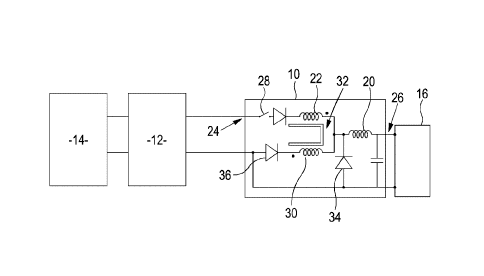
Referring firstly to Figure 2, a DC-DC conversion scheme 10 is illustrated,
the scheme
being arranged to convert a varying DC output from an energy extraction scheme
12 associated with a photovoltaic panel 14 for output via an H-Bridge circuit
16 to, for
example, an electrical supply or distribution network or grid (not shown).
5
The scheme 10 comprises a first inductor 20 connected in series to a second
inductor
22, the first and second inductors 20, 22 connecting an input 24 connected to
the
output of the energy extraction scheme 12 to an output 26 connected to an
input of the
H-Bridge circuit 16. A first switch 28 is located between the input 24 and the
second
10 inductor 22. The first and second inductors 20, 22 are interconnected at
a connection
point to which a third inductor 30 is also connected. The second and third
inductors 22,
30 are wound around a common core 32 and so are magnetically linked to one
another. As a result, a varying current flowing through the second inductor 22
will, in
use, generate a magnetic flux which, in turn, will generate an emf in the
third inductor
30 that induces a current therein. The directions in which the second and
third
inductors 22, 30 are wound is such that the current induced in the third
inductor 30
supplements that flowing through the second inductor 22 when the first switch
28 is
closed.
As illustrated, a second switch 34 in the form of a diode is connected across
the first
inductor 20 and output 26. A further switch 36 also in the form of a diode is
connected
to the third inductor 30 and is operable to control the direction of current
flow through
the third inductor 30. Whilst switches 34, 36 are illustrated as taking the
form of
diodes, it will be appreciated that if desired they could be replaced by other
devices
including appropriately controlled electronic switch devices or the like.
It will be appreciated that the first inductor 20 and first and second
switches 28, 34
together form a Buck converter circuit, the second and third magnetically
linked
inductors 22, 30 together forming a current boost scheme operable to boost the
current
supplied to the first inductor 20 of the Buck converter circuit, in use.
In use, therefore, starting from a condition in which the first switch 28 is
open, it will be
appreciated that no current is flowing from the input 24 to the output 26.
Subsequent
closing of the first switch 28 results in a current starting to flow through
the second
inductor 22 and first inductor 20 to the output 26. The change in current
flowing
CA 02973790 2017-07-13
WO 2016/113559 PCT/GB2016/050073
7
through the second inductor 22 generates a varying magnetic flux. By virtue of
the
magnetic linking of the second and third inductors 22, 30 to one another, the
generated
magnetic flux creates an emf across the third inductor 30. The directions of
the
windings of the second and third inductors 22, 30 are such that the generated
emf
results in the further switch 36, in this case in the form of a diode, turning
on and in a
current being induced, supplementing the current supplied through the second
inductor
22 such that the current supplied to the first inductor 20 is increased.
Depending upon
the level of the generated emf, the diode forming the switch 36 may only
partially turn
on.
The first inductor 20 forms, as mentioned hereinbefore, part of a Buck
converter, the
increased current supplied thereto resulting in energy storage therein in the
usual
manner.
Subsequent reopening of the first switch 28 interrupts the connection of the
second
inductor 22 to the input 24, and a current is no longer supplied to the first
inductor 20
via the second inductor 22. Initially, upon opening of the first switch 28,
the diode
forming the further switch 36 will continue to conduct. During this phase in
the
operation of the scheme, as usual with a Buck converter, the first inductor 20
will
discharge.
As the current supplied to the first inductor 20, in use, is boosted, it will
be appreciated
that to achieve a particular effect at the output 26 the inductance of the
first inductor 20
may be reduced. As a result, the efficiency of the scheme can be enhanced.
As shown in Figure 2, an additional diode 38 may be provided, if desired, to
protect the
first switch 28 from damage or breaking down. It is thought that in relatively
low
voltage applications this may not be required, but that it may be desirable in
higher
voltage applications.
Whilst Figure 2 illustrates the use of the invention in converting the output
from a
photovoltaic panel to a level suitable for use by an electricity supply or
distribution
network or grid, it will be appreciated that the invention may be used in a
number of
other applications. By way of example it may be employed in the power supplies
associated with a wide range of electrical or electronic equipment such as
computer
CA 02973790 2017-07-13
WO 2016/113559 PCT/GB2016/050073
8
equipment, televisions and audio equipment. Furthermore, it could be
incorporated
into the power control systems associated with electric motors such as those
used in
electrically powered vehicles. It will be appreciated that these are merely
examples of
applications in which the invention may be utilised, and that the invention is
not
restricted in this regard.
Figure 4 illustrates a modification to the circuit of Figure 2. In the
modification of Figure
4, a DC link circuit 40 is connected between the buck converter formed, in
part, by the
first inductor 20 and the output 26. The DC link circuit 40 comprises a fourth
inductor
42 and a fifth inductor 44, the fourth and fifth inductors 42, 44 being wound
upon a
common magnetic core and so being magnetically linked to one another. In
addition,
they are electrically connected to one another at a point 46 connected to the
first
inductor 20. The fourth inductor 42 is connected, via a switch 48, to ground,
the fifth
inductor 44 being connected via a diode 50 to the output 26.
In use, when the switch 48 is open, no current flows to ground via the fourth
inductor
42. Upon subsequent opening of the switch 48, current starts to flow through
the fourth
inductor 42. The change in current flowing through the fourth inductor 42
induces a
potential difference across the fifth inductor 44. It
will be appreciated that by
appropriately controlling the opening and closing of the switch 48, the
magnitude of the
output voltage at the output 26 can be controlled. The relationship between
the voltage
at the output 26 and at the input 24 can be expressed as:
V_out/V_in = D_1/(1-D_2/2)
Where Vout and Vin are the voltages at the output 26 and input 24
respectively, and
D1 and D2 represent the proportion of time over which the switches 28 and 48,
respectively, are closed.
It will be appreciated that the modification shown in Figure 4 will be of
particular benefit
in applications in which it is desired to control or vary the magnitude of the
output
voltage, such as in variable speed drive applications. Another advantage of
the
arrangement is that the operation of the circuit does not result in the
generation of
significant harmonics or other effects that require filtration to avoid
negatively impacting
upon the supply.
CA 02973790 2017-07-13
WO 2016/113559 PCT/GB2016/050073
9
Figure 3 illustrates a modification to the arrangement shown in Figure 2 in
which the
second switch 34, instead of being connected to a point between the first and
second
inductors 20, 22, is connected to a point between the switch 28 and the second
inductor 22. Operation of the arrangement of Figure 3 is much the same as that
of
Figure 2 and so will not be described in further detail. If desired, the DC
link circuit of
Figure 4 could be applied to this circuit.
The arrangements described hereinbefore are advantageous in that the circuits
are
simple and incorporate few components. Manufacture thereof may thus be
achieved
economically. If desired, the inductors may be of multi-core form.
It is envisaged that the inductors will be of very small size, for example
each
comprising only a few windings. By way of example, each inductor may have, say
4-6
windings. It will be appreciated, however, that the invention is not
restricted in this
regard.
Referring next to Figure 5, a DC-DC conversion circuit is illustrated that
comprises a
main inductor 110 connected in series with a pair of parallel arms 112, 114,
each arm
112, 114 including a primary inductor 116a, 116b, a secondary inductor 118a,
118b,
and a primary switch 120a, 120b, all arranged in series with one another, and
a
secondary switch 122a, 122b providing a switched ground connection to a point
intermediate the associated primary inductor 116a, 116b and the primary switch
120a,
120b. In the arrangement illustrated, the primary switches 120a, 120b take the
form of
diodes, and so switch on and become conductive depending upon the manner in
which
the circuit is operating. The secondary switches 122a, 122b, whilst
illustrated as
simple switches will typically take the form of suitably controlled electronic
switch
devices such as transistors or transistor-like devices. It will be appreciated
that a wide
range of devices are possible, and the invention is not restricted in this
regard. As
shown in Figure 5, a control unit 124 is provided and controls the operation
of the
secondary switches 122a, 122b.
The primary and secondary inductors 116a, 116b, 118a, 118b of the first and
second
legs 112, 114 are all wound upon a common magnetic core (not shown) and so are
magnetically linked with one another, the winding directions being as
illustrated in
CA 02973790 2017-07-13
WO 2016/113559 PCT/GB2016/050073
Figure 5. The individual inductances of the inductors 116a, 116b, 118a, 118b
are very
low. By way of example, each inductor may be made up of only a few windings.
However, a greater number of windings may be used if desired.
5 With the circuit connected between an input 126 and an output 128, when
both of the
secondary switches 122a, 122b are closed (on), the current flowing through the
main
inductor 110 rises by an amount Ai, inducing an emf in the main inductor 110
opposing
the increase in current. From this condition, when one of the secondary
switches 122a,
122b is opened (off) and the other is closed (on), the current flowing through
the main
10 inductor 110 falls by the amount Ai, the falling current inducing an emf
in the main
inductor 110 in the opposite direction.
By repeatedly opening and closing the secondary switches 122a, 122b, at all
times
ensuring that one or other of the secondary switches 122a, 122b is closed
(on), there
being no times at which both secondary switches 122a, 122b are both open
(off), and
by appropriate selection of the switching frequency, it will be appreciated
that the
current flowing through the main inductor 110 may be continuously changing.
The inductances of the primary and secondary inductors 116a, 116b, 118a, 118b
are
preferably symmetrical in the sense that the inductance of the primary
inductors 116a,
116b are equal to one another, and the inductances of the secondary inductors
118a,
118b are equal to one another. As a consequence, the magnitude of the change
in
current, and the resulting induced emf, will be the same regardless as to
which of the
secondary switches 122a, 122b is operated at any given time.
When both secondary switches 122a, 122b are closed, the potential at point Vn
as
illustrated in Figure 5 is zero, and so
V_in=L_m Ai/t_on
where ton is the duration over which both secondary switches 122a, 122b are
closed,
and using the terminology shown in Figure 5. Figure 7 illustrates the changes
in the
positions of the secondary switches 122a, 122b overtime, identifying those
periods ton
of the period T of the overall switching cycle during which both secondary
switches
CA 02973790 2017-07-13
WO 2016/113559 PCT/GB2016/050073
11
122a, 122b are closed. It is envisaged that the frequency of the switching
cycle will be
in the kHz region, but the invention is not restricted in this regard.
When one or other of the secondary switches 122a, 122b is opened (and the
other is
closed), then Vn is equal to Va, the potential across the primary inductor
116a, 116b of
the leg 112, 114 with which the open secondary switch 122a, 122b is
associated, and
V_in-V_a=K-Wm Ai/(T-t_on )
where T is the period of the switching cycle, as shown in Figure 7.
Defining a duty cycle D as
D=t_on/T
the equations set out above can be solved together to produce the transfer
function
V_outiV_in =(2-Fri) 1/((1-D) )
where
ri=)/(L_b/L_a )==V(L_d/L_c )
It will be appreciated from the expressions set out above that the ratio of
the output
voltage to the input voltage can be controlled by control over the duty cycle,
ie varying
the proportion of time over which both of the secondary switches 122a, 122b
occupies
its closed (on) position, and/or by the selection of the inductances of the
secondary
inductors 118a, 118b relative to the primary inductors 116a, 116b.
The circuit illustrated in Figure 5 may thus serve as a boost circuit,
increasing the
voltage at the output 128 relative to that at the input 126 by a controllable
amount. The
circuit is of very high efficiency, minimal losses being experienced, in use.
Whilst Figure 7 illustrates one possible mode in which the secondary switches
122a,
122b may be controlled, the invention is not restricted in this regard. As
noted above,
CA 02973790 2017-07-13
WO 2016/113559 PCT/GB2016/050073
12
by appropriate control over the duty cycle, the level of boost achieved using
the circuit
may be controlled. Whilst it is particularly advantageous to operate the
circuit in such a
manner that there are no periods of time during which both of the switches are
open
simultaneously, the invention is not restricted in this regard.
Another switching regime that, in some arrangements may be preferred, involves
controlling switching such that the secondary switches 122a, 122b are switched
at
points in the operating cycle at which the potential differences across the
switches
122a, 122b being switched is zero. A number of techniques are possible by
which
such control may be achieved. One possibility is to incorporate an additional
sensing
winding independent of the primary inductors 116a, 116b, but magnetically
associated
therewith, such that that the EMF induced in the sensing winding is related to
the
current flowing within the associated inductors 116a, 116b. By monitoring the
EMF
induced in the sensing winding, it can be determined when the potential
difference
across he switches 122a, 122b are zero, and hence when such zero voltage
switching
should occur.
The circuit of Figure 5 may be modified or reconfigured slightly to serve as a
buck
converter rather than a boost converter.
Figure 6 illustrates the circuit when
reconfigured in this manner. By comparing Figure 5 with Figure 6, it will be
appreciated
that the reconfiguration of the circuit involves switching the input for the
output,
replacing the diodes forming the primary switches 120a, 120b with controllable
switches, and replacing the switches used as the secondary switches 122a, 122b
with
diodes.
The circuit of Figure 6 is operated in substantially the same manner as that
of Figure 5
with the exception that in use the primary switches 120a, 120b, rather than
the
secondary switches 122a, 122b, are positively controlled. The transfer
function of this
circuit can be expressed as
V_out/V_in =D+((1-D))/((2+q) )
It is clear from the transfer function set out above that the circuit of
Figure 6 includes a
buck element (duty cycle D) and an offset related to both the duty cycle and
the ratio of
the inductor values. As with the circuit of Figure 5, therefore, the output
voltage can be
CA 02973790 2017-07-13
WO 2016/113559 PCT/GB2016/050073
13
controlled relative to the input voltage either by controlling the duty cycle
D, by
appropriate control over the operation of the primary switches 120a, 120b, or
by control
over the relative magnitudes of the inductances used in the first and second
legs 112,
114.
Whilst, as with the circuit of Figure 5, the circuit of Figure 6 is preferably
operated in
such a manner that the primary switches 120a, 120b do not both occupy their
open
positions at the same time, the circuit may be operated in such a manner that
this
occurs, if desired.
If both the primary switches 120a, 120b and the secondary switches 122a, 122b
are of
a controllable form, then it will be appreciated that a single circuit may be
produced that
is capable of being used either as a boost converter or as a buck converter,
depending
upon the manner in which it is connected between the input and output and
depending
upon the manner in which it is controlled.
As with the arrangement of Figure 5, the circuit of Figure 6 is preferably
controlled in
such a manner that zero voltage switching thereof occurs.
Figure 8 illustrates an arrangement incorporating the buck circuit of Figure 6
arranged
in series with the boost circuit of Figure 5, the boost and buck circuits
sharing a single
main inductor 110. It will be appreciated that by appropriate control over the
operation
of the switches of the circuit of Figure 8, a universal DC-DC converter scheme
is
provided, allowing the output signal to be controlled in such a manner as to
be high or
lower than the input signal. Such a circuit may be used in a wide range of
applications
including, but not restricted to, applications in which it is desired to
maintain the output
signal at a constant level despite having a varying input signal.
In the circuits described hereinbefore the inductances of the inductors of the
two legs
112, 114 are symmetrically arranged. It will be appreciated that, whilst this
is preferred,
arrangements may be possible in which this is not the case.
The boost and buck converter circuits of Figures 5 and 6 allow the output
signal to be
increased or decreased relative to that at the input with a high degree of
efficiency.
The circuits are relatively simple, and so component costs are relatively low.
CA 02973790 2017-07-13
WO 2016/113559 PCT/GB2016/050073
14
It Will be appreciated that, if desired, the circuits of Figures 5, 6 and 8
may be
incorporated into circuits of the general form shown in Figures 2 and 4.
Whilst the accompanying drawings illustrated specific circuits falling within
the scope of
the invention, it will be understood that a number of modifications or
alternations may
be made thereto without departing from the scope of the invention as defined
by the
appended claims.