Note: Descriptions are shown in the official language in which they were submitted.
MEMS SENSOR WITH ELECTRONICS INTEGRATION
BACKGROUND
[0001] Microelectromechanical systems (MEMS) are small devices comprised
of
electrical and mechanical components, designed to work together to sense
physical properties in
their local environment. For instance, MEMS pressure sensors are designed to
sense and report
the pressure of a fluid or environment in which the pressure sensor resides.
The pressure sensed
by the MEMS pressure sensor, however, results in a very small signal that must
be amplified to
useable levels by electronic components.
[0002] Generally, electronics and MEMS components used in MEMS sensing
devices
are sensitive to errors caused by temperature change and stress. The
temperature sensitivity of
the electronics and MEMS components can be calibrated out by incorporating a
temperature
signal and correcting for temperature. However, there is a limit to how much
can be calibrated
out in a traditional MEMS package configuration, where the electronics are
separated from the
MEMS sensing die. The physical separation allows the electronics and MEMS
sensing die to be
at different temperatures such that the true compensation temperature is not
known. This
uncorrectable temperature difference is particularly high during transient
conditions.
[0003] Some prior art embodiments place electronics on the same silicon
chip on which
the MEMS sensor is located. While this set up can provide overall smaller size
of the device and
higher performance, many MEMS processes are not compatible with complementary
metal-
oxide-semiconductor (CMOS) processing commonly used to create integrated
electronic circuits.
In this setup, overall yields of the devices decrease due to the combining of
yield loss between
the MEMS sensor and the electronics. Additionally, certain components, such as
stabile high
value resistors, are not easily incorporated into CMOS electronics, and the
expense of running
both MEMS and CMOS processes can be quite cost prohibitive.
SUMMARY
[0004] A microelectromechanical sensor device includes a backing wafer,
a
microelectromechanical sensing wafer attached to the backing wafer, a topping
wafer anchored
to the sensing wafer opposite the backing wafer, at least one integrated
circuit component, the at
1
CA 2975342 2017-08-02
least one integrated circuit component bonded to the topping wafer, and a
housing, wherein the
backing wafer is anchored to the housing.
[0005] A method of making a MEMS sensor includes processing a sensor
wafer,
processing a topping wafer, bonding the topping wafer to the sensing wafer,
mounting the
sensing die on a package base, attaching one or more integrated circuit
components to the
topping wafer, and wire bonding the one or more integrated circuit components
to the sensing
wafer.
BRIEF DESCRIPTION OF THE DRAWINGS
[0006] = FIG. 1 is a schematic diagram of a prior art MEMS sensor device.
[0007] FIG. 2A is a schematic diagram of a MEMS sensor device with
electronics
integration.
[0008] FIG. 2B is a schematic diagram of an inertial device with
electronics integration.
[0009] FIG. 3A is a cross-sectional view of a topping wafer in a MEMS
sensor device
with electronics integration.
[0010] FIG. 3B is a cross-sectional view of a topping wafer in a MEMS
sensor
device with electronics integration in a different embodiment with multiple
metal trace layers.
[0011] FIG. 4 is a top-down view of a topping wafer in a MEMS sensor
device with
electronics integration.
[0012] FIG. 5 is a flow chart depicting a method of making a MEMS sensor
device with
electronics integration.
DETAILED DESCRIPTION
[0013] The disclosed system integrates electronic components on to a
topping wafer in
the MEMS sensing die. Incorporating integrated circuit (IC) components and
routing traces into
a topping wafer allows integration of the electronics directly onto the MEMS
sensor. This
minimizes error due to proximity of IC components to the MEMS sensor by
reducing changes in
temperature and stress between the two. Moreover, as MEMS sensors and IC
components are
typically made of silicon substrates and in direct contact, they benefit from
high thermal
conductivity that quickly equilibrates temperatures. Also, since the MEMS
sensor die and
integrated IC components are made out of the same material there is no
thermally induced stress
2
CA 2975342 2017-08-02
due to differences in thermal expansion coefficients. Thus the IC components
and MEMS sensor
stay at nearly the same temperature at all times, even during thermal
transient changes.
[0014] FIG. 1 is a schematic diagram of MEMS sensor device 10 as
disclosed in the prior
art. Prior art device 10 includes sensor die 12, and topping wafer 20; ceramic
board 22;
integrated circuit (IC) components 24; wire bonds 26, 28, 30; electrical
routing 32; feedthrough
pins 34; seal 36; and housing 38, which includes package bade 40, sidewalls
42, and back plate
44.
[0015] In MEMS sensor device 10, sensor die 12 detects pressure of an
external
environment, which can be a fluid or gas. Die 12 includes pedestal 14, backing
wafer 16, sensing
wafer 18, and topping wafer 20. Pedestal 14 can be glass, silicon, or another
suitable material.
Pedestal 14 is anchored to package base 40 of housing 38. Pedestal 14 provides
a path for a fluid
of interest to interact with sensing wafer 18, but prevents stress and damage
from thermal
stresses in package base 40 from reaching sensing wafer 18.
[0016] Backing wafer 16 connects pedestal 14 and sensing wafer 18, and
further protects
sensing wafer 18 from package base 40. Backing wafer 16 can be made of
silicon, and is bonded
to sensing wafer 18 through normal means such as fusion bonding, frit bonding,
eutectic
bonding, anodic bonding, or other appropriate methods. Passage 15 in the
center of backing
wafer 16 allows fluid flow to sensing wafer 18, but is strong enough to
prevent any stress
transmitted through pedestal 14 from affecting sensing wafer 18.
[0017] Sensing wafer 18, which is made of silicon, contains support
portion 17 and
sensing portion 19. Sensing portion 19, located in the center of sensing wafer
18, houses a
diaphragm. When fluid flows from the external environment through pedestal 14
and backing
wafer 16 to sensing wafer 18, it deflects the diaphragm of sensing wafer 18.
When the diaphragm
is deflected, sensing wafer 18 detects pressure of the external fluid compared
to a vacuum or
reference pressure determined by topping wafer 20. Sensing wafer 18 sends a
pressure signal to
IC components 24 through wire bonds 26.
[0018] Topping wafer 20 is typically made of silicon, and is secured on
top of sensing
wafer 18. Topping wafer 20 provides a reference pressure to sensing wafer 18
based on recess 22
in topping wafer 20. Recess 22 can be a vacuum or provide a different
reference pressure.
Topping wafer 20 also prevents sensing wafer 18 from rupturing, by providing
travel stop and
limiting the maximum deflection of the diaphragm.
3
CA 2975342 2017-08-02
=
[0019] Sensor die 12 is connected to IC components 24 by wire bonds 26
and electrical
routing 32. Wire bonds 26 send an electrical signal from sensing wafer 18 to
IC components 24.
In this embodiment, IC components 24 are located on ceramic board 22. Ceramic
board 22 is
secured to package base 40 of housing 38.
[0020] Electrical routing 32 is secured on ceramic board 22. Electrical
routing 32 is
connected to IC components by wire bonds 28, and connected to feedthrough pins
34 by wire
bonds 30. Electrical feedthrough pins 34 run through package base 40 of
housing 38 to an
external receiver (not pictured). Electrical feedthrough pins 34 are sealed to
housing 38 by seal
36.
[0021] The pressure signal from sensing wafer 18 travels to ceramic
board 22 through
wire bonds 26. There, the signal is run through electrical routing 32 and IC
components 24
through wire bonds 28. The signal is amplified by IC components 24 until it is
useable, and then
routed through wire bonds 30 to electrical feedthrough pins 34, where the
signal is routed outside
of housing 38 and device 10 for other use or analysis. One of the many IC
components 24 can
be a temperature detector used to calibrate the device to correct for
temperature errors.
[0022] In this prior art embodiment, sensor die 12 and IC components 24
are separated.
IC components 24 and electrical routing 32 are mounted on ceramic board 22.
For this reason,
housing 38 is very large, and sidewalls 42, package base 40 and back plate 44
must encompass
both sensor die 12 and ceramic board 22. The separation of scrisor die 12 and
IC components 24
also causes an increase in errors due to thermal stresses and temperature
mismatches caused by
distance.
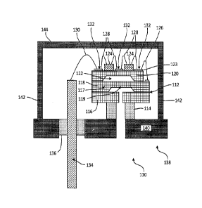
[0023] FIG. 2A is a schematic diagram of MEMS sensor device 110 with
electronics
integration that minimizes the errors associated with the prior art embodiment
shown in FIG. 1.
Device 110 includes sensor die 112, and topping wafer 120; integrated circuit
(IC) components
124; wire bonds 126, 128, 130; electrical routing 132; feedthrough pins 134;
seal 136; and
housing 138, which includes package base 140, sidewalls 142, and back plate
144.
[0024] Sensing die 112 is designed to detect pressure of an external
environment.
Typically, the external environment is a fluid (either liquid or gas). Sensing
die 112 includes
pedestal 114, backing wafer 116, sensing wafer 118, and topping wafer 120.
[0025] Pedestal 114 is open to the external environment, and separates
sensing wafer 118
from foreign object or pressure damage that could occur if sensing wafer 118
was directly
4
CA 2975342 2017-08-02
exposed to the external environment. Pedestal 114 contains a passage allowing
exposure of some
fluid from the external environment to sensing wafer 118, and both insulates
and isolates sensing
wafer 118. Pedestal 114 can be glass, silicon, or other suitable materials.
Pedestal 114 is
mounted on package base 140 of housing 138.
[0026] Backing wafer 116 is mounted on pedestal 114, and further
separates sensing
wafer 118 from package base 140. Backing wafer 116 can be made of silicon.
Backing wafer 116
contains a narrow passage to allow fluid flow to sensing wafer 118 but prevent
foreign object
damage to sensing wafer 118.
[0027] Sensing wafer 118 is designed to measure pressure of the external
environment.
Sensing wafer 118 includes support portions 117 and sensing portion 119.
Support portions 117
are bonded to backing wafer 116 and prevent disruption of sensing portion 119.
Sensing portion
119 can be a piezo resistive or capacitive pressure sensor, and contains a
diaphragm. The
diaphragm is deflected when fluid from the external environment travels
through pedestal 114
and backing wafer 116 to sensing wafer 118. The diaphragm in sensing portion
119 is deflected
relative to the pressure of the fluid from the external environment. Sensing
portion 119 of
sensing wafer 118 sends a signal proportional to the pressure sensed along
wire bond 126 to be
analyzed.
[0028] Topping wafer 120 is bonded to a side of sensing wafer 118
opposite backing
wafer 116. Topping wafer 120 can be made of silicon. Topping wafer 120
contains recess
portion 122 that is centered over sensing portion 119 of sensing wafer 118.
Recess portion 122
provides a reference pressure to sensing wafer 118. The reference pressure can
be a vacuum,
atmospheric pressure, or other appropriate reference pressure.
[0029] In this embodiment, topping wafer 120 replaces a ceramic circuit
board. Instead,
electrical components are bonded to a top side (opposite sensing wafer 118) of
topping wafer
120. This is accomplished by layering dielectric materials and metal traces on
top of topping
wafer 120 in connection layer 123. Connection layer 123 is more fully
discussed in reference to
FIGS. 3A, 3B and 4.
[0030] Electrical routing 132 is bonded to connection layer 123 of
topping wafer 120 to
create electrical connections for IC components 124. Electrical routing 132
can be any
conductive metal traces. IC components 124 can contain any number of required
components,
such as transistors, diodes, resistors, or capacitors, and are typically made
of silicon. IC
CA 2975342 2017-08-02
components 24 can also contain die level passive components, such as precision
resistor chips or
capacitor chips. IC components 24 can contain application specific integrated
circuits (ASICs) or
general purpose integrated circuits. Electrical routing 132 receives a signal
from sensing wafer
118 through wire bond 126, which is then passed to IC components 124 through
wire bonds
128. The signal is amplified by IC components 124 until it is at a useable
level, at which point it
is sent through wire bond 130 to feedthrough pins 134.
[0031] By incorporating electrical routing 132 into connection layer 123
of topping wafer
120, IC components 124 can be incorporated directly on to sensing die 112 of
device 110, and no
additional circuit board (for example, ceramic board 22) is needed within
housing 138. Because
electrical routing 132 and IC components 124 are in the same location as
sensor die 112, thermal
differences between the two are minimized. Moreover, because sensor die 112
and IC
components 124 are typically both made of silicon, and are in direct contact
with each other, they
benefit from high thermal conductivity that quickly equilibrates temperatures.
Also, because
MEMS sensor die 112 and IC components 124 are made out of the same material,
there is no
thermal coefficient of expansion mismatch, resulting in no thermal strain.
This configuration also
minimizes the space required, as no ceramic circuit board needs to be mounted
to housing 138.
[0032] Once the signal is sent to feedthrough pins 134, it is then sent
out of housing 138
to an external receiver (not pictured), where the data can be used or
analyzed. Feedthrough pins
134 can be a singular or multiple feedthrough pins, and can be constructed
with plated Kovar.
Feedthrough pins 134 are sealed to package base 140 of housing 138 by seal 136
to prevent leak
of fluid from the external environment into housing 138 around feedthrough
pins 134. Typically,
seal 136 is a hermetic seal.
[0033] Housing 138 encloses sensing die 112 and IC components 124.
Housing 138
includes package base 140, sidewalls 142, and back plate 144. Housing 138 is
generally made of
steel, nickel, Kovar, or other appropriate plastics, ceramics, metals or
alloys. Pedestal 114 is
anchored to package base 140, and feedthrough pins runs through package base
140, sealed by
hermetic seal 136. Sidewalls 142 and back plate 144 are welded to package base
140 to enclose
device 110.
[0034] This embodiment of a pressure sensor allows for a smaller overall
size of device
110, which is both cost-effective and saves resources. Moreover, this set up
minimizes errors in
the signal that can occur in IC components due to distance and temperature
fluctuations between
6
CA 2975342 2017-08-02
sensing die 112 and IC components 124. This concept can also be applied to
other MEMS
devices.
[0035] For instance, FIG. 2B is a schematic diagram of inertial device
210 with
electronics integration. Device 210 includes sensor die 212, which includes
die attach material
246, backing wafer 216, sensing wafer 218 with proof mass portion 248, and
topping wafer 220;
integrated circuit (IC) components 224; wire bonds 226, 228, 230; electrical
routing 232;
feedthrough pins 234; seal 236; and housing 238, which includes package base
240, sidewalls
242, and back plate 244.
[0036] Inertial device 210 is set up similarly to pressure sensor device
110. The main
components, unless otherwise described, are the same and are connected in the
same fashion.
Inertial device 210 can be an accelerometer, a gyroscope, or other MEMS
inertial device
configured to detect inertia.
[0037] In inertial device 210, die attach material 246 replaces pedestal
114. Die attach
material 246 secures sensing die 212 to housing 238, and can be an epoxy,
solder or eutectic
material. Die attach material 246 is anchored to package base 240 of housing
238. Backing wafer
216 is attached to die attach material 246.
[0038] Backing wafer 216 anchors sensing wafer 218. Backing wafer 216
and sensing
wafer 218 can both be made of silicon, but sensing wafer 218 is the active
MEMS wafer. Unlike
sensing wafer 118 in device 110, sensing wafer 218 here has proof mass portion
248 for inertial
reference.
[0039] Topping wafer 220, which can also be made of silicon, is anchored
to sensing
wafer 218. Similar to topping wafer 120 in FIG. 2A, topping wafer 220 serves
as a circuit board
base for IC components 224 and electrical routing 232. Topping wafer 220
provides a reference
vacuum to sensing wafer 218, or topping wafer 220 can provide a damping
pressure in recess
222 in topping wafer 220. Recess 222 can be a vacuum or provide a reference
pressure to
properly dampen inertial device 210. Electrical components are bonded to a top
side (opposite
sensing wafer 218) of topping wafer 220. This is accomplished by layering
dielectric materials
and metal traces on top of topping wafer 220 in connection layer 223.
Connection layer 223 is
more fully discussed in reference to FIGS. 3A, 3B and 4 (referred to as
connection layer 123A,
123B). As described above, the placement of IC components 224 on topping wafer
220 has a
number of benefits, including decreased signal error and smaller overall size.
7
CA 2975342 2017-08-02
[0040] FIG. 3A is a cross-sectional view of topping wafer 120A in MEMS
sensor device
110 with electronics integration. In this embodiment, topping wafer 120A
includes recess 122A,
and connection layer 123A, which includes bottom dielectric layer 148A, metal
trace layer 150A,
top dielectric layer 152A, and top dielectric layer openings 154A.
[0041] Topping wafer 120A is similar to topping wafers 120 and 220 in
FIGS. 2A and
2B. Topping wafer 120A can be made of silicon, and is anchored to a sensing
wafer, such as 118
or 218. Recess 122A in topping wafer 120A can be centered over sensing portion
119 of sensing
wafer 118 to avoid constraining sensing portion 119. This decouples active
sensing portion 119
of sensing wafer 118 from IC components 124, but still provides high thermal
continuity.
[0042] Topping wafer 120A is covered by a connection layer that includes
layers of
dielectric material and metal traces. In FIG. 3A, connection layer 123A
includes bottom
dielectric layer 148A, metal trace layer 150A, and top dielectric layer 152A.
Dielectric layers
148A and 152A are thin film deposited insulators such as silicon dioxide or
silicon nitride.
Bottom dielectric layer 148A acts as an insulating isolator on a top surface
of topping wafer
120A, similar to ceramic board 22 of FIG. 1. If topping wafer 120A is made out
of an insulating
material, dielectric layer 148A is unnecessary.
[0043] Metal trace layer 150A creates electrical connections above the
top surface of
topping wafer 120A. These electrical connections are accessible by IC
components 124 through
openings 154A in top dielectric layer 152A. Top dielectric layer 152A acts as
a passivation layer
to prevent IC components 124 from shorting. Openings I54A selectively allow
electrical
connections above the top surface of topping wafer 120A.
[0044] FIG. 3B is a cross-sectional view of topping wafer 120B in MEMS
sensor device
110 with electronics integration in a different embodiment. In this
embodiment, topping wafer
120B includes recess 122B, and connection layer 123B, which includes bottom
dielectric layer
148B, first metal trace layer 150B, intermediate dielectric layer 156B,
intermediate dielectric
layer openings 158B, second metal trace layer 160B, top dielectric layer 152B,
and top dielectric
layer openings 154B.
[0045] Topping wafer 120B is similar to topping wafer 120A of FIG. 3A,
but has
additional layers in connection layer 123B based on the needs of the device.
Connection layer
123B includes all the components of connection layer 123A, and additionally
contains
intermediate dielectric layer 156B and second metal trace layer 160B. In this
embodiment,
8
CA 2975342 2017-08-02
openings 158B are made in intermediate dielectric layer 156B. Openings 158B
are filled with
metal trace layer 160B, to allow connection of first metal trace layer 150B
with second metal
trace layer 160B. Openings 154B in top dielectric layer 152B allow metal trace
layers 150B,
160B to electrically connect with IC components 124 or other items on the top
surface of
connection layer 123B.
[0046] FIG. 4 is a top-down view of topping wafer 120 in MEMS sensor
device 110 with
electronics integration. Topping wafer 120 includes IC components 124, metal
traces 150, 160
and top dielectric layer openings 154.
[0047] Topping wafer 120 serves as a platform for a circuit board-like
set up including
IC components 124, metal traces 150, 160, and dielectric layer openings 154.
IC components 124
are wire bonded with metal traces 150, 160 through openings 154. This creates
a circuit that can
receive an incoming signal from sensing wafer 118 via wire bond 126, 226,
amplify the signal,
and send it out through feedthrough pins 134 to external electronics for
further use or analysis.
[0048] FIG. 5 is a flow chart depicting method 300 of making a MEMS
sensor device
with electronics integration. Method 300 begins with processing a sensing
wafer in step 302. The
sensing wafer can be silicon, or alternatively Pyrex, glass, quartz, or other
appropriate materials.
The sensing wafer can include a sensing portion, such as a diaphragm, and a
structural portion.
[0049] Next, in step 304, a topping wafer is processed. The topping wafer
can be silicon.
Once a silicon body of the topping wafer is formed, electrical routes can be
created on a side of
the topping wafer. This includes bonding a first dielectric layer on to a side
of the topping wafer,
then depositing a metal trace layer on top of the first dielectric layer.
Next, a second dielectric
layer is bonded to the metal trace layer. Finally, openings are created in the
second dielectric
layer to allow electrical connection to the metal trace layer. Finally, a
recess is etched into the
topping wafer opposite the side with electrical routes. This can be done
through potassium
hydroxide wet etch methods, or deep reactive ion etching DRIE methods. Step
304 can include
additional steps, such as adding a second metal trace layer and a third
dielectric layer.
[0050] In step 306, the sensing wafer and the topping wafer are bonded
together. They
can be processed individually, or in a batch, through commercially available
methods. A backing
wafer and pedestal can optionally be included. The backing wafer can be made
of silicon, while
the pedestal can be made of an insulating material. The topping wafer, sensing
wafer, backing
wafer and pedestal can be bonded together simultaneously or individually. The
backing wafer is
9
CA 2975342 2017-08-02
anchored to the pedestal, and the sensing wafer is bonded to a side of the
backing wafer opposite
the pedestal. The topping wafer is bonded to a side of the sensing wafer
opposite the backing
wafer. At this point, if the sensor dies are being processed as a batch, they
can be cut into
individual sensor dies.
[0051] Next, in step 308, the sensing die is mounted on a package base.
The package
base is typically steel, nickel, Kovar, or another metallic substance used for
housing a MEMS
device. Generally, the pedestal or backing wafer is mounted directly on the
package base through
a solder preform.
[0052] Next, in step 310, integrated circuit (IC) components are attached
to the topping
wafer. IC components are then wire bonded to metal traces accessible through
the openings in
the top dielectric layer. In step 312, the IC components are wire bonded to
the sensing wafer in
order to receive signals sent by the sensing wafer. Also in step 312, the IC
components can be
wire bonded to one or more electrical feedthrough pins. The feedthrough pins
can be run through
the package base, and sealed with hermetic seals. In the end, the sensor die
and IC components
are enclosed in a housing by welding the package base to sidewalls and a back
plate. Thus, the
sensor die is protected from an external environment.
[0053] The proposed MEMS device with electronics integration places IC
components
on a topping wafer of a sensing die to conserve space, minimize errors and
reduce cost of the
device as a whole. The proposed device reduces the need for ceramic routing
boards and lowers
the complexity and size of the total device, while allowing the device to
provide high
performance. Thermal differences between the MEMS sensor die and the IC
components are
minimized, reducing errors associated with in thermal transient conditions.
Moreover, the
topping wafer decouples the active MEMS sensor region from the IC components
while
providing a high thermal continuity.
[0054] Discussion of Possible Embodiments
[0055] The following are non-exclusive descriptions of possible
embodiments of the
present invention.
[0056] A microelectromechanical sensor device includes a backing wafer, a
microelectromechanical sensing wafer attached to the backing wafer, a topping
wafer anchored
to the sensing wafer opposite the backing wafer, at least one integrated
circuit component, the at
CA 2975342 2017-08-02
least one integrated circuit component bonded to the topping wafer, and a
housing, wherein the
backing wafer is anchored to the housing.
[0057] The device of the preceding paragraph can optionally include,
additionally and/or
alternatively, any one or more of the following features, configurations
and/or additional
components:
[0058] The device includes a pedestal exposed to an external
environment, the backing
wafer secured to the pedestal.
[0059] The pedestal is anchored to the housing.
[0060] The device includes one or more wire bonds connecting the at
least one integrated
circuit component to the sensing wafer.
[0061] The device includes at least one feedthrough pin connected to the
at least one
integrated circuit component through a wire bond.
[0062] The at least one feedthrough pin passes through the housing and
wherein the at
least one feedthrough pin connects to external electronics.
[0063] The housing includes a package base, one or more side walls, and
a back plate.
[0064] The sensing wafer includes a support region and a sensing region.
[0065] The topping wafer contains a recess, the recess positioned over
the sensing region
of the sensing wafer.
[0066] A connection layer is attached to the topping wafer, the
connection layer
comprising: a first dielectric layer attached to a surface of the topping
wafer opposite the sensing
wafer, a first metal trace layer, the first metal trace layer attached to the
first dielectric layer
opposite the topping wafer, and a second dielectric layer, the second
dielectric layer attached to
the first metal trace layer opposite the first dielectric layer.
[0067] The second dielectric layer contains one or more openings.
[0068] The connection layer further comprises a second metal trace layer
connected to
the second dielectric layer opposite the first metal trace layer, and a third
dielectric layer
connected to the second metal trace layer opposite the second dielectric
layer.
[0069] The third dielectric layer contains one or more openings.
[0070] A method of making a MEMS sensor includes processing a sensor
wafer,
processing a topping wafer, bonding the topping wafer to the sensing wafer,
mounting the
sensing die on a package base, attaching one or more integrated circuit
components to the
11
CA 2975342 2017-08-02
topping wafer, and wire bonding the one or more integrated circuit components
to the sensing
wafer.
[0071] The method of the preceding paragraph can optionally include,
additionally
and/or alternatively, any one or more of the following features,
configurations and/or additional
components:
[0072] The method includes bonding a backing wafer to the sensing wafer.
[0073] The method includes bonding a pedestal to the backing wafer and
bonding the
pedestal to a package base.
[0074] The method includes wire bonding the one or more integrated
circuit components
to a feedthrough pin and running the feedthrough pin through an opening in the
package base and
sealing the opening.
[0075] Processing the topping wafer includes bonding a first dielectric
layer on to a side
of the topping wafer, depositing a first metal trace layer on to the first
dielectric layer opposite
the topping wafer, bonding a second dielectric layer on to the first metal
trace layer opposite the
first dielectric layer, and creating openings in the second dielectric layer
such that the first metal
trace layer is reachable through the second dielectric layer.
[0076] Processing the topping wafer includes etching a recess into a
side of the topping
wafer.
[0077] Processing the topping wafer includes depositing a second metal
trace layer on to
the second dielectric layer opposite the first metal trace layer, bonding a
third dielectric layer on
to the second metal trace layer opposite the second dielectric layer, and
creating openings in the
third dielectric layer such that the second metal trace layer is reachable
through the third
dielectric layer.
[0078] While the invention has been described with reference to an
exemplary
embodiment(s), it will be understood by those skilled in the art that various
changes can be made
and equivalents can be substituted for elements thereof without departing from
the scope of the
invention. In addition, many modifications can be made to adapt a particular
situation or
material to the teachings of the invention without departing from the
essential scope thereof.
Therefore, it is intended that the invention not be limited to the particular
embodiment(s)
disclosed, but that the invention will include all embodiments falling within
the scope of the
appended claims.
12
CA 2975342 2017-08-02