Note: Descriptions are shown in the official language in which they were submitted.
POWER TUBE CONNECTION STRUCTURE OF POWER AMPLIFIER
AND POWER AMPLIFIER
TECHNICAL FIELD
The present invention relates to the field of power amplifier technologies,
and in particular, to
a power tube connection structure of a power amplifier and a power amplifier.
BACKGROUND
Conventional power amplifiers include two types: drop-in power amplifiers and
surface mount
power amplifiers. FIG 1 is a schematic structural diagram of a drop-in power
amplifier in the prior
art, including a substrate 01, a printed circuit board 02 covering an upper
surface of the substrate 01,
and a power tube 03. A through groove 04 allowing the power tube 03 to pass
through is cut into the
printed circuit board 02. A mounting groove 05 is cut into the upper surface
of the substrate 01 at a
location that is corresponding to the through groove 04. One end of the power
tube 03 extends
through the through groove 04, and is welded onto a bottom face of the
mounting groove 05.
To make it convenient for the power tube 03 to pass through the through groove
04 and drop in
the mounting groove 05, a size of the mounting groove 05 is 0.25 mm greater
than that of the power
tube 03 on one side. To improve power amplification consistency, assembly
design of a power
amplifier requires that the power tube 03 is pushed toward a side of the
mounting groove that is
close to an output end of the power amplifier, to ensure that there is no gap
left between the output
end of the power amplifier and a side wall of the mounting groove that is
close to the output end of
the power amplifier. However, there is consequently no escape channel for gas
solder flux during
reflow soldering, and a solder void is formed at the bottom of the power tube
03.
CA 2976522 2018-12-12
CA 02976522 2017-08-14
SUMMARY
Embodiments of the present invention provide a power tube connection structure
of a power
amplifier and a power amplifier, to prevent a solder void at the bottom of a
power tube.
To achieve the foregoing objective, according to a first aspect, an embodiment
of the present
invention provides a power tube connection structure of a power amplifier,
including a substrate, a
printed circuit board covering an upper surface of the substrate, and a power
tube, where a through
groove allowing the power tube to pass through is cut into the printed circuit
board, a mounting
groove is cut into the upper surface of the substrate at a location that is
corresponding to the through
groove, one end of the power tube extends through the through groove, and is
welded onto a bottom
face of the mounting groove, the end of the power tube that extends into the
mounting groove abuts
onto a side wall of the mounting groove that is close to an output end of the
power amplifier, and a
solder flux escape channel is made into the side wall of the mounting groove
that is close to the
output end of the power amplifier.
In a first possible implementation manner, with reference to the first aspect,
the solder flux
escape channel is a first opening made into the side wall of the mounting
groove that is close to the
output end of the power amplifier, and there is a gap left between an inner
wall of the through
groove in the printed circuit board and an outer wall of the power tube.
In a second possible implementation manner, with reference to the first
aspect, the solder flux
escape channel is a first opening made into the side wall of the mounting
groove that is close to the
output end of the power amplifier, and a second opening is made into the
printed circuit board at a
location that is corresponding to the first opening.
In a third possible implementation manner, according to the first or the
second possible
implementation manner, the power tube includes a pin laid over an upper
surface of the printed
circuit board, and a through hole is made into the pin at a location that is
corresponding to the first
opening.
In a fourth possible implementation manner, according to the first or the
second possible
implementation manner, the first opening is a semi-circular opening
perpendicular to the bottom
face of the mounting groove.
In a fifth possible implementation manner, with reference to the first aspect,
a side push hole
perpendicular to the bottom face of the mounting groove is made into a side
wall of the mounting
groove that is close to an input end.
In a sixth possible implementation manner, with reference to the first aspect,
multiple
protruding supports are laid in one plane on the bottom face of the mounting
groove, and a height
difference between the protruding supports and the bottom face of the mounting
groove is 0.1-0.2
2
= CA 02976522 2017-08-14
mm.
In a seventh possible implementation manner, according to the sixth possible
implementation
manner, there are four protruding supports, two protruding supports are laid
close to the output end
of the power amplifier, and the rest two protruding supports are laid close to
an input end of the
power amplifier.
According to the power tube connection structure of a power amplifier provided
in this
embodiment of the present invention, a solder flux escape channel is made into
a side wall of a
mounting groove that is close to an output end of a power amplifier, and
during welding, gas solder
flux can flow out of the power amplifier through the solder flux escape
channel, preventing a solder
void from forming at the bottom of a power tube.
According to a second aspect, an embodiment of the present invention provides
a power
amplifier, including the power tube connection structure of a power amplifier
according to any one
of the foregoing technical solutions.
According to the power amplifier provided in this embodiment of the present
invention, a
solder flux escape channel is made into a side wall of a mounting groove that
is close to an output
end of the power amplifier. During welding, gas solder flux can flow out of
the power amplifier
through the solder flux escape channel, preventing a solder void from forming
at the bottom of a
power tube.
BRIEF DESCRIPTION OF DRAWINGS
To describe the technical solutions in the embodiments of the present
invention or in the prior
art more clearly, the following briefly describes the accompanying drawings
required for describing
the embodiments or the prior art. Apparently, the accompanying drawings in the
following
description show merely some embodiments of the present invention, and a
person of ordinary skill
in the art may still derive other drawings from these accompanying drawings
without creative
efforts.
FIG. 1 is a schematic structural diagram of a drop-in power amplifier in the
prior art;
FIG. 2 is a schematic diagram of a power tube connection structure of a power
amplifier
according to an embodiment of the present invention; and
FIG. 3 is a schematic structural diagram of a substrate in a power tube
connection structure of a
power amplifier according to an embodiment of the present invention.
3
CA 02976522 2017-08-14
DESCRIPTION OF EMBODIMENTS
The following clearly and completely describes the technical solutions in the
embodiments of
the present invention with reference to the accompanying drawings in the
embodiments of the
present invention. Apparently, the described embodiments are merely some but
not all of the
embodiments of the present invention. All other embodiments obtained by a
person of ordinary skill
in the art based on the embodiments of the present invention without creative
efforts shall fall
within the protection scope of the present invention.
In the descriptions of the present invention, it should be understood that,
position or location
relationships indicated by the terms "center", "upper", "lower", "ahead",
"behind", "left", "right",
"perpendicular", "horizontal", "top", "bottom", "inner", "outer", and the like
are position or location
relationships based on the accompanying drawings, and are merely intended for
ease of describing
the present invention and simplification of description, instead of indicating
or implying that the
apparatuses or components referred to need to be provided in a particular
position or be constructed
and operated in a particular position, and therefore, shall not be understood
as limitations on the
present invention.
The terms "first" and "second" are merely intended for a purpose of
description, and shall not
be understood as an indication or implication of relative importance or an
implicit indication of a
quantity of indicated technical features. Therefore, a feature modified by
"first" or "second" may
explicitly or implicitly include one or more such features. In the
descriptions of the present
invention, unless otherwise indicated, the meaning of "multiple" is two or
more.
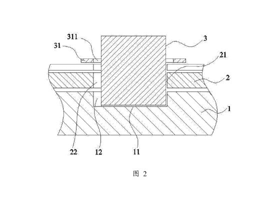
Referring to FIG. 2, FIG 2 shows a specific embodiment of a power tube
connection structure
of a power amplifier according to an embodiment of the present invention. The
power tube
connection structure of a power amplifier includes a substrate 1, a printed
circuit board 2 covering
an upper surface of the substrate 1, and a power tube 3. A through groove 21
allowing the power
tube 3 to pass through is cut into the printed circuit board 2. A mounting
groove 11 is cut into the
upper surface of the substrate 1 at a location that is corresponding to the
through groove 21. One
end of the power tube 3 extends through the through groove 21, and is welded
onto a bottom face of
the mounting groove 11. The end of the power tube 3 that extends into the
mounting groove 11
abuts onto a side wall of the mounting groove 11 that is close to an output
end of the power
amplifier. A solder flux escape channel 12 is made into the side wall of the
mounting groove 11 that
is close to the output end of the power amplifier.
According to the power tube connection structure of a power amplifier provided
in this
embodiment of the present invention, a solder flux escape channel 12 is made
into a side wall of a
mounting groove 11 that is close to an output end of the power amplifier.
During welding, gas
4
CA 02976522 2017-08-14
solder flux can flow out of the power amplifier through the solder flux escape
channel 12,
preventing a solder void from forming at the bottom of a power tube 3.
In an embodiment of the present invention, the solder flux escape channel 12
is a first opening
made into the side wall of the mounting groove 11 that is close to the output
end of the power
amplifier. For the convenience of discharge of gas solder flux, there is a gap
(not shown in the
figure) left between an outer wall of the power tube 3 and an inner wall of
the through groove 21 in
the printed circuit board 2. Gas solder flux flows into the first opening from
the bottom of the power
tube 3, flows from the bottom up in the first opening and flows out from the
top of the first opening,
and is discharged out of the power amplifier through the gap left between the
outer wall of the
power tube 3 and the inner wall of the through groove 21 in the printed
circuit board 2. This is
convenient for discharge of the gas solder flux.
In another embodiment of the present invention, referring to FIG. 2, the
solder flux escape
channel 12 is a first opening made into the side wall of the mounting groove
11 that is close to the
output end of the power amplifier. There is no gap left between an outer wall
of the power tube 3
and an inner wall of the through groove 21 in the printed circuit board 2, but
a second opening 22 is
made into the printed circuit board 2 at a location that is corresponding to
the first opening. In this
case, gas solder flux flows sequentially from the bottom up through the first
opening and the second
opening 22, and is discharged out of the power amplifier from the top of the
second opening 22.
Referring to FIG 2, the power tube 3 usually includes a pin 31 laid over an
upper surface of
the printed circuit board 2, while the pin 31 blocks discharge of gas solder
flux to a degree. In order
that the gas solder flux is discharged more smoothly, a through hole 311 is
made into the pin 31 at a
location that is corresponding to the first opening. In this way, the blocking
effect of the pin 31 on
the gas solder flux is reduced, and therefore, discharge of the gas solder
flux is smoother.
To reduce difficulty of processing, the first opening is a semi-circular
opening perpendicular to
the bottom face of the mounting groove 11. For the substrate 1, a semi-
circular chamfer is usually
processed by using a milling technology, and therefore, the semi-circular
opening may be processed
by using the same technology. This reduces processing steps and therefore
reduces the difficulty of
processing.
Referring to FIG. 3, to make it convenient to push the power tube 3 toward a
side of the
mounting groove 11 that is close to the output end of the power amplifier, a
side push hole 13
perpendicular to the bottom face of the mounting groove 11 is made into a side
wall of the
mounting groove 11 that is close to an input end. A cylindrical pin may be
inserted into the side
push hole 13. As the cylindrical pin is inserted, the cylindrical pin may
squeeze an edge of the
power tube 3, so that the power tube 3 moves toward the side of the mounting
groove 11 that is
5
CAA 02976522 2017-08-14
close to the output end of the power amplifier, until there is no gap left
between the output end of
the power amplifier and the side wall of the mounting groove 11 that is close
to the output end of
the power amplifier.
Different materials are used for the substrate 1 and the power tube 3 whose
thermal expansion
rates also vary greatly. As a result, tearing is likely to occur during
welding, damaging the materials.
Therefore, as shown in FIG 3, multiple protruding supports 14 are laid in one
plane on the bottom
face of the mounting groove 11. A height difference between the protruding
supports 14 and the
bottom face of the mounting groove 11 is 0.1-0.2 mm. The protruding supports
14 provide support
for the power tube 3, making room for distortion buffer between the substrate
1 and the power tube
3. This reduces the occurrence of tearing.
To improve welding precision between the substrate I and the power tube 3,
there are four
protruding supports 14. Two protruding supports 14 are laid close to the
output end of the power
amplifier. The rest two protruding supports 14 are laid close to an input end
of the power amplifier.
In this way, the power tube 3 and the substrate 1 are parallel to each other,
and solder is more
evenly fed during welding. Therefore, the welding precision between the
substrate 1 and the power
tube 3 is improved.
An embodiment of the present invention further provides a power amplifier,
including the
power tube connection structure of a power amplifier according to any one of
the foregoing
embodiments.
According to the power amplifier provided in this embodiment of the present
invention, a
solder flux escape channel 12 is made into a side wall of a mounting groove 11
that is close to an
output end of the power amplifier. During welding, gas solder flux can flow
out of the power
amplifier through the solder flux escape channel 12, preventing a solder void
from forming at the
bottom of a power tube 3.
Other components and the like of the power amplifier in this embodiment of the
present
invention are well known to a person skilled in the art, and details are not
described herein.
The foregoing descriptions are merely specific implementation manners of the
present
invention, but are not intended to limit the protection scope of the present
invention. Any variation
or replacement readily figured out by a person skilled in the art within the
technical scope disclosed
in the present invention shall fall within the protection scope of the present
invention. Therefore, the
protection scope of the present invention shall be subject to the protection
scope of the claims.
6