Note: Descriptions are shown in the official language in which they were submitted.
VARIABLE OPTIC OPHTHALMIC DEVICE INCLUDING
LIQUID CRYSTAL ELEMENTS
CROSS REFERENCE TO RELATED APPLICATIONS
This patent application claims the benefit of U.S. Patent Application Serial
No. 15/245,532 filed August 24, 2016.
BACKGROUND OF THE INVENTION
1. Field of the Invention
The present invention describes an ophthalmic lens device with a variable
optic capability and, more specifically, in some embodiments, the fabrication
of an
ophthalmic lens with a variable optic insert utilizing liquid crystal
elements.
2. Discussion of the Related Art
Traditionally an ophthalmic lens, such as a contact lens or an intraocular
lens provided a predetermined optical quality. A contact lens, for example,
may
provide one or more of the following: vision correcting functionality;
cosmetic
enhancement; and therapeutic effects, but only a set of vision correction
functions. Each function is provided by a physical characteristic of the lens.
Basically, a design incorporating a refractive quality into a lens provides
vision
corrective functionality. A pigment incorporated into the lens may provide a
cosmetic enhancement. An active agent incorporated into a lens may provide a
therapeutic functionality.
To date, optical quality in an ophthalmic lens has been designed into the
physical characteristic of the lens. Generally, an optical design has been
determined and then imparted into the lens during fabrication of the lens, for
example through cast molding, or lathing. The optical qualities of the lens
have
1
CAN_DMS: \ 108358478 \ 1
CA 2976680 2017-08-16
remained static once the lens has been formed. However, wearers may at times
find it beneficial to have more than one focal power available to them in
order to
provide sight accommodation. Unlike spectacle wearers, who can change
spectacles to change an optical correction, contact wearers or those with
intraocular lenses have not been able to change the optical characteristics of
their
vision correction without significant effort.
SUMMARY OF THE INVENTION
Accordingly, the present invention includes innovations relating to a
variable optic insert with liquid crystal elements that may be energized and
incorporated into an ophthalmic device, which is capable of changing the
optical
quality of the lens. Examples of such ophthalmic devices may include a contact
lens or an intraocular lens. In addition, methods and apparatus for forming an
ophthalmic lens with a variable optic insert with liquid crystal elements are
presented. Some embodiments may also include a cast-molded silicone hydrogel
contact lens with a rigid or formable energized insert, which additionally
includes a
variable optic portion, wherein the insert is included within the ophthalmic
lens in a
biocompatible fashion.
The present invention therefore includes disclosure of an ophthalmic lens
with a variable optic insert, apparatus for forming an ophthalmic lens with a
variable optic insert, and methods for manufacturing the same. An energy
source
may be deposited onto a variable optic insert and the insert may be placed in
proximity to one, or both of, a first mold part and a second mold part. A
reactive
monomer mixture is placed between the first mold part and the second mold
part.
The first mold part is positioned proximate to the second mold part thereby
forming a lens cavity with the energized media insert and at least some of the
reactive monomer mixture in the lens cavity; the reactive monomer mixture is
exposed to actinic radiation to form an ophthalmic lens. Lenses are formed via
the
control of actinic radiation to which the reactive monomer mixture is exposed.
In
some embodiments, an ophthalmic lens skirt or an insert-encapsulating layer
may
2
CA 2976680 2017-08-16
, . .
be comprised of standard hydrogel ophthalmic lens formulations. Exemplary
materials with characteristics that may provide an acceptable match to
numerous
insert materials may include, for example, the Narafilcon family(including
Narafilcon A and Narafilcon B), the Etafilcon family(including Etafilcon A),
Galyfilcon A and Senofilcon A.
The methods of forming the variable optic insert with liquid crystal elements
and the resulting inserts are important aspects of various embodiments. In
some
embodiments, the liquid crystal may be located between two alignment layers,
which may set the resting orientation for the liquid crystal. Those two
alignment
layers may be in electrical communication with an energy source through
electrodes deposited on substrate layers that contain the variable optic
portion.
The electrodes may be energized through an intermediate interconnect to an
energy source or directly through components embedded in the insert.
The energization of the alignment layers may cause a shift in the liquid
crystal from a resting orientation to an energized orientation. In embodiments
that
operate with two levels of energization, on or off, the liquid crystal may
only have
one energized orientation. In other alternative embodiments, where
energization
occurs along a scale of energy levels, the liquid crystal may have multiple
energized orientations.
The resulting alignment and orientation of the molecules may affect light
that passes through the liquid crystal layer thereby causing the variation in
the
variable optic insert. For example, the alignment and orientation may act with
refractive characteristics upon the incident light. Additionally, the effect
may
include alteration of polarization of the light. Some embodiments may include
a
variable optic insert wherein energization alters a focal characteristic of
the lens.
In some embodiments, a dielectric material may be deposited between an
alignment layer and an electrode. Such embodiments may include dielectric
material with three-dimensional characteristics such as, for example, a
preformed
shape. Other embodiments may include a second layer of dielectric material
wherein the first layer of dielectric material varies in thickness across the
region
3
CA 2976680 2017-08-16
within the optical zone resulting in a varying electric field across the layer
of liquid
crystal material. In alternate embodiments, the ophthalmic lens device may
include a first layer of dielectric material that may be a composite of two
materials
with similar optical characteristics and dissimilar low frequency dielectric
characteristics.
BRIEF DESCRIPTION OF THE DRAWINGS
The foregoing and other features and advantages of the invention will be
apparent from the following, more particular description of preferred
embodiments
of the invention, as illustrated in the accompanying drawings.
Figure 1 illustrates exemplary mold assembly apparatus components that
may be useful in implementing some embodiments of the present invention.
Figures 2A and 2B illustrate an exemplary energized ophthalmic lens with a
variable optic insert embodiment.
Figure 3 illustrates a cross sectional view of a variable optic insert where
the front and back curve pieces of the variable optic insert may have
different
curvature and wherein the variable optic portion may be comprised of liquid
crystal.
Figure 4 illustrates a cross sectional view of an ophthalmic lens device
embodiment with a variable optic insert wherein the variable optic portion may
be
comprised of liquid crystal
Figure 5 illustrates an exemplary embodiment or a variable optic insert
wherein the variable optic portion may be comprised of liquid crystal.
Figure 6 illustrates an alternative exemplary embodiment of a variable optic
insert
wherein the variable optic portions may be comprised of liquid crystal.
Figure 7 illustrates method steps for forming an ophthalmic lens with a
variable optic insert which may be comprised of liquid crystal.
Figure 8 illustrates an example of apparatus components for placing a
variable optic insert comprised of liquid crystal into an ophthalmic lens mold
part.
4
CA 2976680 2017-08-16
Figure 9 illustrates a processor that may be used to implement some
embodiments of the present invention.
Figure 10 illustrates an alternative exemplary embodiment of a variable
optic insert wherein the variable optic portion may be comprised of liquid
crystal.
Figure 11 illustrates an alternative exemplary embodiment of a variable
optic insert wherein the variable optic portion may be comprised of liquid
crystal.
Figures 12A-B illustrate an alternative exemplary embodiment of a variable
optic insert wherein the variable optic portion may be comprised of liquid
crystal.
Figures 13A-C illustrate an alternative exemplary embodiment of a variable
optic insert wherein the variable optic portion may be comprised of liquid
crystal.
Figures 14A-B illustrate an alternative exemplary embodiment of a variable
optic insert wherein the variable optic portion may be comprised of liquid
crystal.
Figure 15 illustrates an alternative exemplary embodiment of a variable
optic insert wherein the variable optic portion may be comprised of liquid
crystal.
Figures 16A-B illustrate an alternative exemplary embodiment of a variable
optic insert wherein the variable optic portion may be comprised of liquid
crystal.
Figures 17A-B illustrate an alternative exemplary embodiment of a variable
optic insert wherein the variable optic portion may be comprised of liquid
crystal.
Figures 17C, D, E illustrate an alternative exemplary embodiment of an
alignment layer for an exemplary embodiment of a variable optic insert wherein
the variable optic portion may be comprised of liquid crystal. Figure 17F
illustrates an alternative exemplary embodiment of a variable optic insert
wherein
the variable optic portion may be comprised of liquid crystal and equations of
merit for the type of embodiment.
Figures 18 and 18A illustrates an exemplary embodiment of patterning of
liquid crystals and exemplary optical results deriving from a device of said
type.
Figure 19A and 19B illustrate an alternative exemplary embodiment of
patterning
of liquid crystals which may be incorporated into variable optic inserts.
Figure 20 illustrates a close-up of the embodiments of the type illustrated in
Figure 19.
5
CA 2976680 2017-08-16
Figures 21, 21A, 21B and 21C illustrate an alternative exemplary
embodiment of a variable optic insert wherein the variable optic portion may
be
comprised of liquid crystal.
Figures 22, 22A, 22B and 22 C illustrate an alternative exemplary
embodiment of a variable optic insert wherein the variable optic portion may
be
comprised of liquid crystal.
Figure 23 illustrates an alternative exemplary embodiment of a variable
optic insert wherein the variable optic portion may be comprised of liquid
crystal
and the manner that polarized light components may be affected while
traversing
the embodiment.
DETAILED DESCRIPTION OF THE INVENTION
The present invention includes methods and apparatuses for
manufacturing an ophthalmic lens with a variable optic insert wherein the
variable
optic portion is comprised of a liquid crystal. In addition, the present
invention
includes an ophthalmic lens with a variable optic insert comprised of liquid
crystal
incorporated into the ophthalmic lens.
According to the present invention, an ophthalmic lens is formed with an
embedded insert and an energy source, such as an electrochemical cell or
battery
as the storage means for the energy. In some exemplary embodiments, the
materials comprising the energy source may be encapsulated and isolated from
an environment into which an ophthalmic lens is placed.
A wearer-controlled adjustment device may be used to vary the optic
portion. The adjustment device may include, for example, an electronic device
or
passive device for increasing or decreasing a voltage output. Some exemplary
embodiments may also include an automated adjustment device to change the
variable optic portion via an automated apparatus according to a measured
parameter or a wearer input. Wearer input may include, for example, a switch
controlled by wireless apparatus. Wireless may include, for example, radio
6
CA 2976680 2017-08-16
. .
frequency control, magnetic switching, and inductance switching. In other
exemplary embodiments activation may occur in response to a biological
function
or in response to a measurement of a sensing element within the ophthalmic
lens.
Other exemplary embodiments may result from the activation being triggered by
a
change in ambient lighting conditions as a non-limiting example.
In some exemplary embodiments, the insert also includes a variable optic
portion comprised of liquid crystal layers. The variation in optic power may
occur
when electric fields, created by the energization of electrodes, causes
realignment
within the liquid crystal layer thereby shifting the molecules from the
resting
orientation to an energized orientation. In other alternative exemplary
embodiments, different effects caused by the alteration of liquid crystal
layers by
energization of electrodes may be exploited, for example, rotation of
polarizing
angles.
In some exemplary embodiments with liquid crystal layers, there may be
elements in the non-optical zone portion of the ophthalmic lens that may be
energized, whereas other exemplary embodiments may not require energization.
In the embodiments without energization, the liquid crystal may be passively
variable based on some exterior factor, for example, ambient temperature, or
ambient light.
A liquid crystal lens may provide an electrically variable index of refraction
to polarized light incident upon its body. A combination of two lenses where
the
axis of polarization is rotated in the second lens relative to the first lens
allows for
a lens element that may be able to vary the index of refraction to ambient non-
polarized light.
By combining electrically active liquid crystal layers with electrodes, a
physical entity may be achieved that may be controlled by applying an
electrical
field across the electrodes. If there is a dielectric layer that is present on
the
periphery of the liquid crystal layer then the field across the dielectric
layer and the
field across the liquid crystal layer may combine into the field across the
electrodes. In a three dimensional shape the nature of the combination of the
7
CA 2976680 2017-08-16
, . .
fields across the layers may be estimated based on electrodynamic principals
and
the geometry of the dielectric layer and the liquid crystal layer. If the
effective
electrical thickness of the dielectric layer is made in a non-uniform manner
then
the effect of a field across the electrodes may be "shaped" by the effective
shape
of the dielectric and create dimensionally shaped changes in refractive index
in
the liquid crystal layers. In some exemplary embodiments, such shaping may
result in lenses that have the ability to adopt variable focal
characteristics.
An alternative exemplary embodiment may derive when the physical lens
elements that contain the liquid crystal layers are shaped themselves to have
different focal characteristics. The electrically variable index of refraction
of a
liquid crystal layer may then be used to introduce changes in focal
characteristics
of the lens based on the application of an electric field across the liquid
crystal
layer through the use of electrodes. The shape that the front containment
surface
makes with the liquid crystal layer and the shape that the back containment
surface makes with the liquid crystal layer may determine to first order the
focal
characteristics of the system.
In the following sections, detailed descriptions of exemplary embodiments
of the invention will be given. The description of both preferred and
alternative
embodiments are exemplary embodiments only, and it is understood that to those
skilled in the art that variations, modifications and alterations may be
apparent. It
is therefore to be understood that the exemplary embodiments do not limit the
scope of the underlying invention.
GLOSSARY
In this description and claims directed to the presented invention, various
terms may be used for which the following definitions will apply:
Alignment layer: as used herein refers to a layer adjacent to a liquid crystal
layer that influences and aligns the orientation of molecules within the
liquid crystal
layer. The resulting alignment and orientation of the molecules may affect
light that
8
CA 2976680 2017-08-16
passes through the liquid crystal layer. For example, the alignment and
orientation
may act with refractive characteristics upon the incident light. Additionally,
the
effect may include alteration of polarization of the light.
Electrical Communication: as used herein refers to being influenced by an
electrical field. In the case of conductive materials, the influence may
result from or
in the flow of electrical current. In other materials, it may be an electrical
potential
field that causes an influence, such as the tendency to orient permanent and
induced molecular dipoles along field lines as an example.
Energized: as used herein refers to the state of being able to supply
electrical current to or to have electrical energy stored within.
Energized orientation: as used herein refers to the orientation of the
molecules of a liquid crystal when influenced by an effect of a potential
field
powered by an energy source. For example, a device containing liquid crystals
may have one energized orientation if the energy source operates as either on
or
off. In other embodiments, the energized orientation may change along a scale
affected by the amount of Energy applied.
Energy: as used herein refers to the capacity of a physical system to do
work. Many uses within this invention may relate to the said capacity being
able to
perform electrical actions in doing work.
Energy source: as used herein refers to device capable of supplying
Energy or placing a biomedical device in an Energized state.
Energy Harvesters: as used herein refers to device capable of extracting
energy from the environment and convert it to electrical energy.
Intraocular lens: as used herein refers to an ophthalmic lens that is
embedded within the eye.
Lens-Forming Mixture or Reactive Mixture or reactive monomer mixture
(RMM): as used herein refers to a monomer or prepolymer material that can be
cured and crosslinked or crosslinked to form an ophthalmic lens. Various
embodiments may include lens-forming mixtures with one or more additives such
9
CA 2976680 2017-08-16
as: UV blockers, tints, photoinitiators or catalysts, and other additives one
might
desire in an ophthalmic lens, for example, contact or intraocular lenses.
Lens-Forming Surface: as used herein refers to a surface that is used to
mold a lens. In some embodiments, any such surface may have an optical quality
surface finish, which indicates that it is sufficiently smooth and formed so
that a
lens surface fashioned by the polymerization of a lens-forming mixture in
contact
with the molding surface is optically acceptable. Further, in some
embodiments,
the lens-forming surface may have a geometry that is necessary to impart to
the
lens surface the desired optical characteristics, including, for example,
spherical,
aspherical and cylinder power, wave front aberration correction, and corneal
topography correction.
Liquid Crystal: as used herein refers to a state of matter having properties
between a conventional liquid and a solid crystal. A liquid crystal cannot be
characterized as a solid but its molecules exhibit some degree of alignment.
As
used herein, a liquid crystal is not limited to a particular phase or
structure, but a
liquid crystal may have a specific resting orientation. The orientation and
phases
of a liquid crystal may be manipulated by external forces, for example,
temperature, magnetism, or electricity, depending on the class of liquid
crystal.
Lithium Ion Cell: as used herein refers to an electrochemical cell where
Lithium ions move through the cell to generate electrical energy. This
electrochemical cell, typically called a battery, may be reenergized or
recharged in
its typical forms.
Media insert or insert: as used herein refers to a formable or rigid substrate
capable of supporting an energy source within an ophthalmic lens. In some
exemplary embodiments, the media insert also includes one or more variable
optic
portions.
Mold: as used herein refers to a rigid or semi-rigid object that may be used
to form lenses from uncured formulations. Some preferred molds include two
mold
parts forming a front curve mold part and a back curve mold part.
CA 2976680 2017-08-16
Ophthalmic Lens or Lens: as used herein refers to any ophthalmic device
that resides in or on the eye. These devices may provide optical correction or
may
be cosmetic. For example, the term lens can refer to a contact lens,
intraocular
lens, overlay lens, ocular insert, optical insert, or other similar device
through
which vision is corrected or modified, or through which eye physiology is
cosmetically enhanced (e.g. iris color) without impeding vision. In some
exemplary
embodiments, the preferred lenses of the invention are soft contact lenses
which
are made from silicone elastomers or hydrogels, which include, for example,
silicone hydrogels and fluorohydrogels.
Optical zone: as used herein refers to an area of an ophthalmic lens
through which a wearer of the ophthalmic lens sees.
Power: as used herein refers to work done or energy transferred per unit of
time.
Rechargeable or Reenergizable: as used herein refers to a capability of
being restored to a state with higher capacity to do work. Many uses within
this
invention may relate to the capability of being restored with the ability to
flow
electrical current at a certain rate for certain, reestablished time period.
Reenergize or Recharge: as used herein refers to the restoration of an
energy source to a state with higher capacity to do work. Many uses within
this
invention may relate to restoring a device to the capability to flow
electrical current
at a certain rate for a certain, reestablished time period.
Released from a mold: as used herein refers to a lens is either completely
separated from the mold, or is only loosely attached so that it can be removed
with mild agitation or pushed off with a swab.
Resting orientation: as used herein refers to the orientation of the
molecules of a liquid crystal device in its resting, non-energized state.
Variable optic: as used herein refers to the capacity to change an optical
quality, such as, for example, the optical power of a lens or the polarizing
angle.
11
CA 2976680 2017-08-16
OPHTHALMIC LENSES
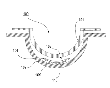
Referring to Figure 1, an apparatus 100 to form ophthalmic devices
comprising sealed and encapsulated inserts is depicted. The apparatus includes
an exemplary front curve mold 102 and a matching back curve mold 101. A
variable optic insert 104 and a body 103 of the ophthalmic device may be
located
inside the front curve mold 102 and the back curve mold 101. In some exemplary
embodiments, the material of the hydrogel body 103 may be a hydrogel material,
and the variable optic insert 104 may be surrounded on all surfaces by this
material.
The variable optic insert 104 may comprise multiple liquid crystal layers
109 and 110. Other exemplary embodiments may include a single liquid crystal
layer, some of which are discussed in later sections. The use of the apparatus
100 may create a novel ophthalmic device comprised of a combination of
components with numerous sealed regions.
In some exemplary embodiments, a lens with a variable optic insert 104
may include a rigid center soft skirt design wherein a central rigid optical
element
including the liquid crystal layers 109 and 110 is in direct contact with the
atmosphere and the corneal surface on respective anterior and posterior
surfaces.
The soft skirt of lens material (typically a hydrogel material) is attached to
a
periphery of the rigid optical element, and the rigid optical element may also
add
energy and functionality to the resulting ophthalmic lens.
Referring to Figure 2A, at 200 a top down and Figure 2B at 250 a cross
sectional depiction of an exemplary embodiment of a variable optic insert is
shown. In this depiction, an energy source 210 is shown in a periphery portion
211 of the variable optic insert 200. The energy source 210 may include, for
example, a thin film, rechargeable lithium ion battery or an alkaline cell
based
battery. The energy source 210 may be connected to interconnect features 214
to
allow for interconnection. Additional interconnects at 225 and 230, for
example,
may connect the energy source 210 to a circuit such as item 205. In other
12
CA 2976680 2017-08-16
exemplary embodiments, an insert may have interconnect features deposited on
its surface.
In some exemplary embodiments, the variable optic insert 200 may include
a flexible substrate. This flexible substrate may be formed into a shape
approximating a typical lens form in a similar manner previously discussed or
by
other means. However to add additional flexibility, the variable optic insert
200
may include additional shape features such as radial cuts along its length.
There
may be multiple electronic components such as that indicated by 205 such as
integrated circuits, discrete components, passive components and such devices
that may also be included.
A variable optic portion 220 is also illustrated. The variable optic portion
may be varied on command through the application of a current through the
variable optic insert. In some exemplary embodiments, the variable optic
portion
220 is comprised of a thin layer of liquid crystal between two layers of
transparent
substrate. There may be numerous manners of electrically activating and
controlling the variable optic component, typically through action of the
electronic
circuit 205. The electronic circuit, may receive signals in various manners
and
may also connect to sensing elements which may also be in the insert such as
item 215. In some embodiments, the variable optic insert may be encapsulated
into a lens skirt 255, which may be comprised of hydrogel material or other
suitable material to form an ophthalmic lens. In these exemplary embodiments
the ophthalmic lens may be comprised of the ophthalmic skirt 255 and an
encapsulated ophthalmic lens insert 200 which may itself comprise layers or
regions of liquid crystal material or comprising liquid crystal material.
A VARIABLE OPTIC INSERT INCLUDING LIQUID CRYSTAL ELEMENTS
Referring to Figure 3, item 300, an illustration of the lens effect of two
differently shaped lens pieces may be found. As mentioned previously, a
variable
optic insert of the inventive art herein may be formed by enclosing an
electrode
and liquid crystal layer system within two differently shaped lens pieces. The
13
CA 2976680 2017-08-16
electrode and liquid crystal layer system may occupy a space between the lens
pieces as illustrated at 350. At 320 a front curve piece may be found and at
310 a
rear curve piece may be found.
In a non-limiting example, the front curve piece 320 may have a concave
shaped surface that interacts with the space 350. The shape may be further
characterized as having a radius of curvature depicted as 330 and a focal
point
335 in some embodiments. Other more complicated shapes with various
parametric characteristics may be formed within the scope of the inventive
art;
however, for illustration a simple spherical shape may be depicted.
In a similar and also non-limiting fashion, the back curve piece 310 may
have a convex shaped surface that interacts with the space 350. The shape may
be further characterized as having a radius of curvature depicted as 340 and a
focal point 345 in some embodiments. Other more complicated shapes with
various parametric characteristics may be formed within the scope of the
inventive
art; however, for illustration a simple spherical shape may be depicted.
To illustrate how the lens of the type as 300 may operate, the material that
comprises items 310 and 320 may have a natural index of refraction of a
predetermined value, within the space 350 the liquid crystal layer may be
chosen
in a non-limiting example to match that predetermined value for the index of
refraction. Thus when light rays traverse the lens pieces 310 and 320 and the
space 350, they will not react to the various interfaces in a manner that
would
adjust the focal characteristics. In its function, portions of the lens not
shown may
activate an energization of various components that may result in the liquid
crystal
layer in space 350 assuming a different index of refraction to the incident
light ray.
In a non-limiting example, the resulting index of refraction may be lowered.
Now,
at each material interface the path of the light may be modeled to be altered
based on the focal characteristics of the surface and the change of the index
of
refraction.
The model may be based on Snell's law: sin (thetai) / sin (theta2) = n2in1.
For example, the interface may be formed by piece 320 and space 350. Thetai
14
CA 2976680 2017-08-16
may be the angle that the incident ray makes with a surface normal at the
interface. Theta2 may be the modeled angle that the ray makes with a surface
normal as it leaves the interface. n2 may represent the index of refraction of
the
space 350 and n1 may represent the index of refraction of the piece 320. When
n1
is not equal to n2 then the angles thetai and theta2 will be different as
well. Thus,
when the electrically variable index of refraction of the liquid crystal layer
in space
350 is changed, the path that a light ray would take at the interface will
change as
well.
Referring to Figure 4, an ophthalmic lens 400 is shown with an embedded
variable optic insert 410. The ophthalmic lens 400 may have a front curve
surface
401 and a back curve surface 402. The insert 410 may have a variable optic
portion 403 with a liquid crystal layer 404. In some exemplary embodiments,
the
insert 410 may have multiple liquid crystal layers 404 and 405. Portions of
the
insert 410 may overlap with the optical zone of the ophthalmic lens 400.
Referring to Figure 5, a variable optic portion 500 that may be inserted into
an ophthalmic lens is illustrated with a liquid crystal layer 530. The
variable optic
portion 500 may have a similar diversity of materials and structural relevance
as
has been discussed in other sections of this specification. In some exemplary
embodiments, a transparent electrode 545 may be placed on the first
transparent
substrate 550. The first lens surface 540 may be comprised of a dielectric
film,
and in some exemplary embodiments, alignment layers which may be placed
upon the first transparent electrode 545. In such exemplary embodiments, the
shape of the dielectric layer of the first lens surface 540 may form a
regionally
varied shape in the dielectric thickness as depicted. Such a regionally varied
shape may introduce additional focusing power of the lens element above the
geometric effects discussed in reference to Figure 3. In some embodiments, for
example, the shaped layer may be formed by injection molding upon the first
transparent electrode 545 substrate 550 combination.
In some exemplary embodiments the first transparent electrode 545 and
the second transparent electrode 520 may be shaped in various manners. In
CA 2976680 2017-08-16
some examples, the shaping may result in separate distinct regions being
formed
that may have energization applied separately. In other examples, the
electrodes
may be formed into patterns such as a helix from the center of the lens to the
periphery which may apply a variable electric field across the liquid crystal
layer
530. In either case, such electrode shaping may be performed in addition to
the
shaping of dielectric layer upon the electrode or instead of such shaping. The
shaping of electrodes in these manners may also introduce additional focusing
power of the lens element under operation.
A liquid crystal layer 530 may be located between the first transparent
electrode 545 and a second transparent electrode 525. The second transparent
electrode 525 may be attached to the top substrate layer 510, wherein the
device
formed from top substrate layer 510 to the bottom substrate layer 550 may
comprise the variable optic portion 500 of the ophthalmic lens. Two alignment
layers may also be located at 540 and 525 upon the dielectric layer and may
surround the liquid crystal layer 525. The alignment layers at 540 and 525 may
function to define a resting orientation of the ophthalmic lens. In some
exemplary
embodiments, the electrode layers 525 and 545 may be in electrical
communication with liquid crystal layer 530 and cause a shift in orientation
from
the resting orientation to at least one energized orientation.
Referring to Figure 6, an alternative of a variable optic insert 600 that may
be inserted into an ophthalmic lens is illustrated with two liquid crystal
layers 620
and 640. Each of the aspects of the various layers around the liquid crystal
region
may have similar diversity as described in relation to the variable optic
insert 500
in Figure 5. In some exemplary embodiments, the alignment layers may introduce
polarization sensitivity into the function of a single liquid crystal element.
By
combining a first liquid crystal based element formed by a first substrate
610,
whose intervening layers in the space around 620 and a second substrate 630
may have a first polarization preference, with a second liquid crystal based
element formed by a second surface on the second substrate 630, the
intervening layers in the space around 640 and a third substrate 650 with a
16
CA 2976680 2017-08-16
,
second polarization preference, a combination may be formed which may allow
for an electrically variable focal characteristic of a lens that is not
sensitive to the
polarization aspects of incident light upon it.
At the exemplary element 600, a combination of two electrically active
liquid crystal layers of the various types and diversity associated with the
example
at 500 may be formed utilizing three substrate layers. In other examples, the
device may be formed by the combination of four different substrates. In such
examples, the intermediate substrate 630 may be split into two layers. If the
substrates are combined at a later time, a device that functions similarly to
item
600 may result. The combination of four layers may present a convenient
example
for the manufacturing of the element where similar devices may be constructed
around both 620 and 640 liquid crystal layers where the processing difference
may relate to the portion of steps that define alignment features for the
liquid
crystal element. In still further examples, if the lens element around a
single liquid
crystal layer such that depicted at 500 is spherically symmetric or symmetric
upon
a rotation of ninety degrees, then two pieces may be assembled into a
structure
of the type depicted at 600 by rotating the two pieces ninety degrees relative
to
each other before assembling.
MATERIALS
Microinjection molding embodiments may include, for example, a poly(4-
methylpent-1-ene) copolymer resin are used to form lenses with a diameter of
between about 6 mm to 10 mm and a front surface radius of between about 6 mm
and 10 mm and a rear surface radius of between about 6 mm and 10 mm and a
center thickness of between about 0.050 mm and 1.0 mm. Some exemplary
embodiments include an insert with diameter of about 8.9 mm and a front
surface
radius of about 7.9 mm and a rear surface radius of about 7.8 mm and a center
thickness of about 0.200 mm and an edge profile of about 0.050 radius.
The variable optic insert 104 may be placed in a mold part 101 and 102
utilized to form an ophthalmic lens. Mold part 101 and mold part 102 material
17
CA 2976680 2017-08-16
= =
may include, for example: a polyolefin of one or more of: polypropylene,
polystyrene, polyethylene, polymethyl methacrylate, and modified polyolefins.
Other molds may include a ceramic or metallic material.
A preferred alicyclic co-polymer contains two different alicyclic polymers.
Various grades of alicyclic co-polymers may have glass transition temperatures
ranging from 105 C to 160 C.
In some exemplary embodiments, the molds of the present invention may
include polymers such as polypropylene, polyethylene, polystyrene, polymethyl
methacrylate, modified polyolefins containing an alicyclic moiety in the main
chain
and cyclic polyolefins. This blend may be used on either or both mold halves,
where it is preferred that this blend is used on the back curve and the front
curve
consists of the alicyclic co-polymers.
In some preferred methods of making molds 100 according to the present
invention, injection molding is utilized according to known techniques,
however,
exemplary embodiments may also include molds fashioned by other techniques
including, for example, lathing, diamond turning, or laser cutting.
Typically, lenses are formed on at least one surface of both mold parts 101
and 102. However, in some exemplary embodiments, one surface of a lens may
be formed from a mold part 101 or 102 and another surface of a lens may be
formed using a lathing method, or other methods.
In some exemplary embodiments, a preferred lens material includes a
silicone containing component. A "silicone-containing component" is one that
contains at least one [-Si-0-] unit in a monomer, macromer or prepolymer.
Preferably, the total Si and attached 0 are present in the silicone-containing
component in an amount greater than about 20 weight percent, and more
preferably greater than 30 weight percent of the total molecular weight of the
silicone-containing component. Useful silicone-containing components
preferably
comprise polymerizable functional groups such as acrylate, methacrylate,
acrylamide, methacrylamide, vinyl, N-vinyl lactam, N-vinylamide, and styryl
functional groups.
18
CA 2976680 2017-08-16
. =
In some exemplary embodiments, the ophthalmic lens skirt, also called an
insert-encapsulating layer, that surrounds the insert may be comprised of
standard hydrogel ophthalmic lens formulations. Exemplary materials with
characteristics that may provide an acceptable match to numerous insert
materials may include, but are not limited to, the Narafilcon family(including
Narafilcon A and Narafilcon B), and the Etafilcon family(including Etafilcon
A). A
more technically inclusive discussion follows on the nature of materials
consistent
with the art herein. One ordinarily skilled in the art may recognize that
other
material other than those discussed may also form an acceptable enclosure or
partial enclosure of the sealed and encapsulated inserts and should be
considered consistent and included within the scope of the claims.
Suitable silicone containing components include compounds of Formula I
R1 R1 R1
Ri¨Si¨O¨Si¨O¨Si¨R1
i
R' R'-b R'
where
R1 is independently selected from monovalent reactive groups, monovalent
alkyl groups, or monovalent aryl groups, any of the foregoing which may
further
comprise functionality selected from hydroxy, amino, oxa, carboxy, alkyl
carboxy,
alkoxy, amido, carbamate, carbonate, halogen or combinations thereof; and
monovalent siloxane chains comprising 1-100 Si-0 repeat units which may
further
comprise functionality selected from alkyl, hydroxy, amino, oxa, carboxy,
alkyl
carboxy, alkoxy, amido, carbamate, halogen or combinations thereof;
where b = 0 to 500, where it is understood that when b is other than 0, b is
a distribution having a mode equal to a stated value;
wherein at least one R1 comprises a monovalent reactive group, and in
some embodiments between one and 3 R1 comprise monovalent reactive groups.
19
CA 2976680 2017-08-16
As used herein "monovalent reactive groups" are groups that can undergo
free radical and/or cationic polymerization. Non-limiting examples of free
radical
reactive groups include (meth)acrylates, styryls, vinyls, vinyl ethers,
C1_6a1ky1(meth)acrylates, (meth)acrylamides, C1_6alkyl(meth)acrylamides, N-
vinyllactams, N-vinylamides, C2_12alkenyls, C2_12alkenylphenyls,
C2_12alkenylnaphthyls, C2_6alkenylphenylC1_6alkyls, 0-vinylcarbamates and 0-
vinylcarbonates. Non-limiting examples of cationic reactive groups include
vinyl
ethers or epoxide groups and mixtures thereof. In one embodiment the free
radical reactive groups comprises (meth)acrylate, acryloxy, (meth)acrylamide,
and
mixtures thereof.
Suitable monovalent alkyl and aryl groups include unsubstituted
monovalent Ci to Cisalkyl groups, C6-C1.4 aryl groups, such as substituted and
unsubstituted methyl, ethyl, propyl, butyl, 2-hydroxypropyl, propoxypropyl,
polyethyleneoxypropyl, combinations thereof and the like.
In one embodiment, b is zero, one R1 is a monovalent reactive group, and
at least 3 R1 are selected from monovalent alkyl groups having one to 16
carbon
atoms, and in another embodiment from monovalent alkyl groups having one to 6
carbon atoms. Non-limiting examples of silicone components of this embodiment
include 2-methyl-,2-hydroxy-3-[3-[1,3,3,3-tetramethy1-1-
[(trimethylsilyl)oxy]disiloxanyl]propoxy]propyl ester ("SIGMA"),
2-hydroxy-3-methacryloxypropyloxypropyl-tris(trimethylsiloxy)silane,
3-methacryloxypropyltris(trimethylsiloxy)silane ("TRIS"),
3-methacryloxypropylbis(trimethylsiloxy)methylsilane and
3-methacryloxypropylpentamethyl disiloxane.
In another embodiment, b is 2 to 20, 3 to 15 or in some embodiments 3 to
10; at least one terminal R1 comprises a monovalent reactive group and the
remaining R1 are selected from monovalent alkyl groups having 1 to 16 carbon
atoms, and in another embodiment from monovalent alkyl groups having 1 to 6
carbon atoms. In yet another embodiment, b is 3 to 15, one terminal R1
comprises
a monovalent reactive group, the other terminal R1 comprises a monovalent
alkyl
CA 2976680 2017-08-16
group having 1 to 6 carbon atoms and the remaining R1 comprise monovalent
alkyl group having 1 to 3 carbon atoms. Non-limiting examples of silicone
components of this embodiment include (mono-(2-hydroxy-3-methacryloxypropyI)-
propyl ether terminated polydimethylsiloxane (400-1000 MW)) ("OH-mPDMS"),
monomethacryloxypropyl terminated mono-n-butyl terminated
polydimethylsiloxanes (800-1000 MW), ("mPDMS").
In another embodiment, b is 5 to 400 or from 10 to 300, both terminal R1
comprise monovalent reactive groups and the remaining R1 are independently
selected from monovalent alkyl groups having 1 to 18 carbon atoms, which may
have ether linkages between carbon atoms and may further comprise halogen.
In one embodiment, where a silicone hydrogel lens is desired, the lens of
the present invention will be made from a Reactive Mixture comprising at least
about 20 and preferably between about 20 and 70%wt silicone containing
components based on total weight of reactive monomer components from which
the polymer is made.
In another embodiment, one to four R1 comprises a vinyl carbonate or
carbamate of the formula:
Formula II
0
H2C=C¨(CH2)q-0¨C¨Y
wherein: Y denotes Om S- or NH-;
R denotes, hydrogen or methyl; d is 1, 2, 3 or 4; and q is 0 or 1.
The silicone-containing vinyl carbonate or vinyl carbamate monomers
specifically include: 1,3-bis[4-(vinyloxycarbonyloxy)but-1-yl]tetramethyl-
disiloxane;
3-(vinyloxycarbonylthio) propyl-[tris (trimethylsiloxy)silane]; 3-
[tris(trimethylsiloxy)silyl] propyl allyl carbamate; 3-
[tris(trimethylsiloxy)silyl] propyl
vinyl carbamate; trimethylsilylethyl vinyl carbonate; trimethylsilylmethyl
vinyl
carbonate, and
21
CA 2976680 2017-08-16
,
O
CH3 CH3 CH3 0
H2C=-C-OCO(CH3)4-Si 0 ___________ Si ¨O __ Si (CH2)4000¨C=CH2
CH3 CH3 CH3
-25
Where biomedical devices with modulus below about 200 are desired, only
one R1 shall comprise a monovalent reactive group and no more than two of the
remaining R1 groups will comprise monovalent siloxane groups.
Another class of silicone-containing components includes polyurethane
macromers of the following formulae:
Formulae IV-VI
(*D*A*D*G)a *D*D*El;
E(*D*G*D*A)a *D*G*D*E1 or;
E(*D*A*D*G)a *D*A*D*E1
wherein:
D denotes an alkyl diradical, an alkyl cycloalkyl diradical, a cycloalkyl
diradical, an aryl diradical or an alkylaryl diradical having 6 to 30 carbon
atoms,
G denotes an alkyl diradical, a cycloalkyl diradical, an alkyl cycloalkyl
diradical, an aryl diradical or an alkylaryl diradical having 1 to 40 carbon
atoms
and which may contain ether, thio or amine linkages in the main chain;
* denotes a urethane or ureido linkage;
a is at least 1;
A denotes a divalent polymeric radical of formula:
Formula VII
-R11-- R11
I I
¨(CH2)y-SiO-Si-(CF12)y-
FIR 1 1 R111
22
CA 2976680 2017-08-16
R11 independently denotes an alkyl or fluoro-substituted alkyl group having 1
to10
carbon atoms, which may contain ether linkages between carbon atoms; y is at
least 1; and p provides a moiety weight of 400 to 10,000; each of E and E1
independently denotes a polymerizable unsaturated organic radical represented
by formula:
Formula VIII
R12
R13CI-C¨(CH2)w¨(X)x¨(Z)z¨(Ar)y¨R14¨
wherein: R12 is hydrogen or methyl; R13 is hydrogen, an alkyl radical having 1
to 6
carbon atoms, or a ¨CO¨Y¨R16 radical wherein Y is ¨0¨,Y¨s¨ or ¨NH¨;
R14 is a divalent radical having 1 to 12 carbon atoms; X denotes ¨CO¨ or ¨
000¨; Z denotes ¨0¨ or ¨NH¨, Ar denotes an aromatic radical having 6 to
30 carbon atoms; w is 0 to 6; x is 0 or 1; y is 0 or 1; and z is 0 or 1.
A preferred silicone-containing component is a polyurethane macromer
represented by the following formula:
Formula IX
90 9 9 9 õ 4 0
1)1
0-13 CH3 - 0 0
11 11 CH3
C H2= C-- COCH2C - cc R16- NCCC H2CH,OCH2CH,OCN- R16- NCC(CH2)
Si¨ (CH2),3,- OCN- R16- NOCCH2CH2OCH,CH,OCN¨ R16¨ NCO¨ CH,CH,C00 CH,
CH, H H H H11 1 1 1 1
0-13 PCH3 H H H H
a
wherein R16 is a diradical of a diisocyanate after removal of the isocyanate
group,
such as the diradical of isophorone diisocyanate. Another suitable silicone
containing macromer is compound of formula X (in which x + y is a number in
the
range of 10 to 30) formed by the reaction of fluoroether, hydroxy-terminated
polydimethylsiloxane, isophorone diisocyanate and isocyanatoethylmethacrylate.
23
CA 2976680 2017-08-16
Formula X
0
O
----- NH -11- 0 (SiMe20)25 S WI NH 0
NH OCH2CF2 (0CF2)¨(0CF2CF 2),
¨ OCF2CH20
0 0
."-----')'yO'"----''NH-11---0(SiMe20)25SiMe20)L NH
0
0 = NH
Other silicone containing components suitable for use in this invention
include macromers containing polysiloxane, polyalkylene ether, diisocyanate,
polyfluorinated hydrocarbon, polyfluorinated ether and polysaccharide groups;
polysiloxanes with a polar fluorinated graft or side group having a hydrogen
atom
attached to a terminal difluoro-substituted carbon atom; hydrophilic siloxanyl
methacrylates containing ether and siloxanyl linkanges and crosslinkable
monomers containing polyether and polysiloxanyl groups. Any of the foregoing
polysiloxanes can also be used as the silicone containing component in this
invention.
LIQUID CRYSTAL MATERIALS
There may be numerous materials that may have characteristics consistent
with the liquid crystal layer types that have been discussed herein. It may be
expected that liquid crystal materials with favorable toxicity may be
preferred and
naturally derived cholesteryl based liquid crystal materials may be useful. In
other
examples, the encapsulation technology and materials of ophthalmic inserts may
allow a broad choice of materials that may include the LCD display related
materials which may typically be of the broad categories related to nematic or
cholesteric N* or smectic C* liquid crystals or liquid crystal mixture.
Commercially
available mixtures such as Merck Specialty chemicals, Licristal mixtures for
TN,
VA, PSVA, IPS and FFS applications and other commercially available mixtures
may form a material choice to form a liquid crystal layer.
24
CA 2976680 2017-08-16
In a non-limiting sense, mixtures or formulations may contain the following
liquid crystal materials: 1-(trans-4-Hexylcyclohexyl)-4-isothiocyanatobenzene
liquid crystal, benzoic acid compounds including (4-Octylbenzoic acid and 4-
Hexylbenzoic acid), carbonitrile compounds including(41-Penty1-4-
biphenylcarbonitrile, 4'-Octy1-4-biphenylcarbonitrile, 4'-(Octyloxy)-4-
biphenylcarbonitrile, 4'-(Hexyloxy)-4-biphenylcarbonitrile, 4-(trans-4-
Pentylcyclohexyl)benzonitrile, 4'-(Pentyloxy)-4-biphenylcarbonitrile, 4'-Hexy1-
4-
biphenylcarbonitrile) , and 4,4'-Azoxyanisole.
In a non-limiting sense, a formulation which may be referred to as W1825
may be used as a liquid crystal layer forming material. W1825 may be as
available from BEAM Engineering for Advanced Measurements Co. (BEAMCO).
There may be other classes of liquid crystal materials that may be useful
for the inventive concepts here. For example, ferroelectric liquid crystals
may
provide function for electric field oriented liquid crystal embodiments, but
may also
introduce other effects such as magnetic field interactions. Interactions of
electromagnetic radiation with the materials may also differ.
ALIGNMENT LAYER MATERIALS:
In many of the exemplary embodiments that have been described, the
liquid crystal layers within ophthalmic lenses may need to be aligned in
various
manners at insert boundaries. The alignment, for example, may be parallel or
perpendicular to the boundaries of the inserts, and this alignment may be
obtained by proper processing of the various surfaces. The processing may
involve coating the substrates of the inserts that contain the liquid crystal
(LC) by
alignment layers. Those alignment layers are described herein.
A technique commonly practiced in liquid crystal based devices of various
types may be a rubbing technique. These techniques may be adapted to account
for the curved surfaces such as the ones of the insert pieces used for
enclosing
the liquid crystal. In an example, the surfaces may be coated by a Polyvinyl
Alcohol (PVA) layer. For example, a PVA layer may be spin coated using a 1
CA 2976680 2017-08-16
. ,
wt.% aqueous solution. The solution may be applied with spin coating at 1000
rpm for time such as approximately 60 s, and then dried. Subsequently, the
dried layer may then be rubbed by a soft cloth. In a non-limiting example, the
soft
cloth may be velvet.
Photo-alignment may be another technique for producing alignment layers
upon liquid crystal enclosures. In some exemplary embodiments, photo-
alignment may be desirable due to its non-contact nature and the capability of
large scale fabrication. In a non-limiting example, the photo-alignment layer
used
in the liquid crystal variable optic portion may be comprised of a dichroic
azobenzene dye (azo dye) capable of aligning predominantly in the direction
perpendicular to the polarization of linear polarized light of typically UV
wavelengths. Such alignment may be a result of repetitive trans-cis-trans
photoisomerization processes.
As an example, PAAD series azobenzene dyes may be spin coated from a
1 wt.% solution in DMF at 3000 rpm for 30 s. Subsequently, the obtained layer
may be exposed to a linear polarized light beam of a UV wavelength (such as
for
example, 325 nm, 351 nm, 365 nm) or even a visible wavelength (400-500 nm).
The source of the light may take various forms. In some exemplary embodiments,
light may originate from laser sources for example. Other light sources such
as
LEDs, halogen and incandescent sources may be other non-limiting examples.
Either before or after the various forms of light are polarized in the various
patterns as appropriate, the light may be collimated in various manners such
as
through the use of optical lensing devices. Light from a laser source may
inherently have a degree of collimation, for example.
A large variety of photoanisotropic materials are known currently, based on
azobenzene polymers, polyesthers, photo-crosslinkable polymer liquid crystals
with mesogenic 4-(4-methoxycinnamoyloxy)biphenyl side groups and the like.
Examples of such materials include sulfonic bisazodye SD1 and other
azobenzene dyes, particularly, PAAD-series materials available from BEAM
26
CA 2976680 2017-08-16
Engineering for Advanced Measurements Co. (BEAMCO), Poly(vinyl cinnamates),
and others.
In some exemplary embodiments, it may be desirable to use water or
alcohol solutions of PAAD series azo dyes. Some azobenzene dyes, for example,
Methyl Red, may be used for photoalignment by directly doping a Liquid Crystal
layer. Exposure of the azobenzene dye to a polarized light may cause diffusion
and adhesion of the azo dyes to and within the bulk of the liquid crystal
layer to
the boundary layers creating desired alignment conditions.
Azobenzene dyes such as Methyl Red may also be used in combination
with a polymer, for example, PVA. Other photoanisotropic materials capable of
enforcing alignment of adjacent layers of liquid crystals may be acceptable
are
known currently. These examples may include materials based on coumarines,
polyesthers, photo-crosslinkable polymer liquid crystals with mesogenic 4-(4-
methoxycinnamoyloxy) -biphenyl side groups, Poly(vinyl cinnamates), and
others.
The photo-alignment technology may be advantageous for embodiments
comprising patterned orientation of liquid crystal.
In another exemplary embodiment of producing alignment layers, the
alignment layer may be obtained by vacuum deposition of silicon oxide on the
insert piece substrates. For example, Si02 may be deposited at low pressure
such
as ¨10-6 mbar. It may be possible to provide alignment features at a
nanoscaled
size that are injection molded into with the creation of the front and back
insert
pieces. These molded features may be coated in various manners with the
materials that have been mentioned or other materials that may directly
interact
with physical alignment features and transmit the alignment patterning into
alignment orientation of liquid crystal molecules.
Still further exemplary embodiments may relate to the creation of physical
alignment features to the insert pieces after they are formed. Rubbing
techniques
as are common in other liquid crystal based art may be performed upon the
molded surfaces to create physical grooves. The surfaces may also be subjected
to a post molding embossing process to create small grooved features upon
them.
27
CA 2976680 2017-08-16
Still further exemplary embodiments may derive from the use of etching
techniques which may involve optical patterning processes of various kinds.
DIELECTRIC MATERIALS
Dielectric films and dielectrics are described herein. By way of non-limiting
examples, the dielectric film or dielectrics used in the liquid crystal
variable optic
portion possess characteristics appropriate to the invention described herein.
A
dielectric may comprise one or more material layers functioning alone or
together
as a dielectric. Multiple layers may be used to achieve dielectric performance
superior to that of a single dielectric.
The dielectric may permit a defect-free insulating layer at a thickness
desired for the discretely variable optic portion, for example, between 1 and
10
pm. A defect may be referred to as a pinhole, as is known by those skilled in
the
art to be a hole in the dielectric permitting electrical and/or chemical
contact
through the dielectric. The dielectric, at a given thickness, may meet
requirements
for breakdown voltage, for example, that the dielectric should withstand 100
volts
or more.
The dielectric may allow for fabrication onto curved, conical, spherical, and
complex three-dimensional surfaces (e.g., curved surfaces or non-planar
surfaces). Typical methods of dip- and spin-coating may be used, or other
methods may be employed.
The dielectric may resist damage from chemicals in the variable optic
portion, for example, the liquid crystal or liquid crystal mixture, solvents,
acids,
and bases or other materials that may be present in the formation of the
liquid
crystal region. The dielectric may resist damage from infrared, ultraviolet,
and
visible light. Undesirable damage may include degradation to parameters
described herein, for example, breakdown voltage and optical transmission. The
dielectric may resist permeation of ions. The dielectric may adhere to an
underlying electrode and/or substrate, for example, with the use of an
adhesion
promotion layer. The dielectric may be fabricated using a process which allows
for
28
CA 2976680 2017-08-16
low contamination, low surface defects, conformal coating, and low surface
roughness.
The dielectric may possess relative permittivity or a dielectric constant
which is compatible with electrical operation of the system, for example, a
low
relative permittivity to reduce capacitance for a given electrode area. The
dielectric may possess high resistivity, thereby permitting a very small
current to
flow even with high applied voltage. The dielectric may possess qualities
desired
for an optic device, for example, high transmission, low dispersion, and
refractive
index within a certain range.
Exemplary, non-limiting, dielectric materials, include one or more of Parylene-
C,
Parylene-HT, Silicon Dioxide, Silicon Nitride, and Teflon AF.
ELECTRODE MATERIALS
Electrodes are described herein for applying an electric potential for
achieving an electric field across the liquid crystal region. An electrode
generally
comprises one or more material layers functioning alone or together as an
electrode.
The electrode may adhere to an underlying substrate, dielectric coating, or
other objects in the system, perhaps with the use of an adhesion promoter
(e.g.,
methacryloxypropyltrimethoxysilane). The electrode may form a beneficial
native
oxide or be processed to create a beneficial oxide layer. The electrode may be
transparent, substantially transparent or opaque, with high optical
transmission
and little reflection. The electrode may be patterned or etched with known
processing methods. For example, the electrodes may be evaporated, sputtered,
or electroplated, using photolithographic patterning and/or lift-off
processes.
The electrode may be designed to have suitable resistivity for use in the
electrical system described herein, for example, meeting the requirements for
resistance in a given geometric construct.
The electrodes may be manufactured from any suitable material, including
one or more of indium tin oxide (ITO), gold, stainless steel, chrome,
graphene,
29
CA 2976680 2017-08-16
,
graphene doped layers and aluminum . It will be appreciated that this is not
an
exhaustive list.
PROCESSES
The following method steps are provided as examples of processes that
may be implemented according to some aspects of the present invention. It
should be understood that the order in which the method steps are presented is
not meant to be limiting and other orders may be used to implement the
invention.
In addition, not all of the steps are required to implement the present
invention
and additional steps may be included in various exemplary embodiments of the
present invention. It may be obvious to one skilled in the art that additional
exemplary embodiments may be practical, and such methods are well within the
scope of the claims.
Referring to Figure 7, a flowchart illustrates exemplary steps that may be
used to implement the present invention. At 701, form a first substrate layer
the
first substrate layer may comprise a back curve surface and have a top surface
with a shape of a first type that may differ from the shape of surface of
other
substrate layers, and, at 702, form a second substrate layer which may
comprise
a front curve surface or an intermediate surface or a portion of an
intermediate
surface for more complicated devices. At 703, an electrode layer may be
deposited upon the first substrate layer. The deposition may occur, for
example,
by vapor deposition or electroplating. In some exemplary embodiments, the
first
substrate layer may be part of an insert that has regions both in the optical
zone
and regions in the non-optic zone. The electrode deposition process may
simultaneously define interconnect features in some exemplary embodiments.
At 704, the first substrate layer may be further processed to add an
alignment layer upon the previously deposited electrode layer. The alignment
layers may be deposited upon the top layer on the substrate and then processed
in standard manners, for example, rubbing techniques, to create the grooving
features that are characteristic of standard alignment layers or by treatment
with
CA 2976680 2017-08-16
exposure to energetic particles or light. Thin layers of reactive mesogens may
be
processed with light exposure to form alignment layers with various
characteristics.
At 705, the second substrate layer may be further processed. An electrode
layer may be deposited upon the second substrate layer in an analogous fashion
to step 703. Then in some exemplary embodiments, at 706, a dielectric layer
may
be applied upon the second substrate layer upon the electrode layer. The
dielectric layer may be formed to have a variable thickness across its
surface. As
an example, the dielectric layer may be molded upon the first substrate layer.
Alternatively, a previously formed dielectric layer may be adhered upon the
electrode surface of the second substrate piece.
At 707, an alignment layer may be formed upon the second substrate layer
in similar fashion to the processing step at 704. After 707, two separate
substrate
layers that may form at least a portion of an ophthalmic lens insert may be
ready
to be joined. In some exemplary embodiments at 708, the two pieces will be
brought in close proximity to each other and then liquid crystal material may
be
filled in between the pieces. At 709, the two pieces may be brought adjacent
to
each other and then sealed to form a variable optic element with liquid
crystal.
In some exemplary embodiments, two pieces of the type formed at 709
may be created by repeating method steps 701 to 709 wherein the alignment
layers are offset from each other to allow for a lens that may adjust the
focal
power of non-polarized light. In such exemplary embodiments, the two variable
optic layers may be combined to form a single variable optic insert. At 710,
the
variable optic portion may be connected to the energy source and intermediate
or
attached components may be placed thereon.
At 711, the variable optic insert resulting at step 710 may be placed within
a mold part. The variable optic insert may or may not also contain one or more
components. In some preferred embodiments, the variable optic insert is placed
in
the mold part via mechanical placement. Mechanical placement may include, for
example, a robot or other automation, such as that known in the industry to
place
31
CA 2976680 2017-08-16
= . .
surface mount components. Human placement of a variable optic insert is also
within the scope of the present invention. Accordingly, any mechanical
placement
or automation may be utilized which is effective to place a variable optic
insert
with an energy source within a cast mold part such that the polymerization of
a
reactive mixture contained by the mold part will include the variable optic in
a
resultant ophthalmic lens.
In some exemplary embodiments, a variable optic insert is placed in a mold
part attached to a substrate. An energy source and one or more components are
also attached to the substrate and are in electrical communication with the
variable optic insert. Components may include, for example, circuitry to
control
power applied to the variable optic insert. Accordingly, in some exemplary
embodiments a component includes a control mechanism for actuating the
variable optic insert to change one or more optical characteristics, for
example, a
change of state between a first optical power and a second optical power.
In some exemplary embodiments, a processor device, MEMS, NEMS or
other component may also be placed into the variable optic insert and in
electrical
contact with the energy source. At 712, a reactive monomer mixture may be
deposited into a mold part. At 713, the variable optic insert may be
positioned into
contact with the reactive mixture. In some exemplary embodiments the order of
placement of variable optic and depositing of monomer mixture may be reversed.
At 714, the first mold part is placed proximate to a second mold part to form
a
lens-forming cavity with at least some of the reactive monomer mixture and the
variable optic insert in the cavity. As discussed above, preferred embodiments
include an energy source and one or more components also within the cavity and
in electrical communication with the variable optic insert.
At 715, the reactive monomer mixture within the cavity is polymerized.
Polymerization may be accomplished, for example, via exposure to one or both
of
actinic radiation and heat. At 716, the ophthalmic lens is removed from the
mold
parts with the variable optic insert adhered to or encapsulated within the
insert-
encapsulating polymerized material making up the ophthalmic lens.
32
CA 2976680 2017-08-16
Although the invention herein may be used to provide hard or soft contact
lenses made of any known lens material, or material suitable for manufacturing
such lenses, preferably, the lenses of the invention are soft contact lenses
having
water contents of about 0 to about 90 percent. More preferably, the lenses are
made of monomers containing hydroxy groups, carboxyl groups, or both or be
made from silicone-containing polymers, such as siloxanes, hydrogels, silicone
hydrogels, and combinations thereof. Material useful for forming the lenses of
the
invention may be made by reacting blends of macromers, monomers, and
combinations thereof along with additives such as polymerization initiators.
Suitable materials include, without limitation, silicone hydrogels made from
silicone macromers and hydrophilic monomers.
APPARATUS
Referring now to Figure 8, automated apparatus 810 is illustrated with one
or more transfer interfaces 811. Multiple mold parts, each with an associated
variable optic insert 814 are contained on a pallet 813 and presented to
transfer
interfaces 811. Embodiments, may include, for example, a single interface
individually placing variable optic insert 814, or multiple interfaces (not
shown)
simultaneously placing variable optic inserts 814 into the multiple mold
parts, and
in some embodiments, in each mold part. Placement may occur via vertical
movement 815 of the transfer interfaces 811.
Another aspect of some embodiments of the present invention includes
apparatus to support the variable optic insert 814 while the body of the
ophthalmic
lens is molded around these components. In some embodiments the variable
optic insert 814 and an energy source may affixed to holding points in a lens
mold
(not illustrated). The holding points may be affixed with polymerized material
of
the same type that will be formed into the lens body. Other exemplary
embodiments include a layer of prepolymer within the mold part onto which the
variable optic insert 814 and an energy source may be affixed.
33
CA 2976680 2017-08-16
,
PROCESSORS INCLUDED IN INSERT DEVICES
Referring now to Figure 9, a controller 900 is illustrated that may be used in
some exemplary embodiments of the present invention. The controller 900
includes a processor 910, which may include one or more processor components
coupled to a communication device 920. In some embodiments, a controller 900
may be used to transmit energy to the energy source placed in the ophthalmic
lens.
The controller 900 may include one or more processors, coupled to a
communication device configured to communicate energy via a communication
channel. The communication device may be used to electronically control one or
more of the placement of a variable optic insert into the ophthalmic lens or
the
transfer of a command to operate a variable optic device.
The communication device 920 may also be used to communicate, for
example, with one or more controller apparatus or manufacturing equipment
components.
The processor 910 is also in communication with a storage device 930.
The storage device 930 may comprise any appropriate information storage
device, including combinations of magnetic storage devices (e.g., magnetic
tape
and hard disk drives), optical storage devices, and/or semiconductor memory
devices such as Random Access Memory (RAM) devices and Read Only Memory
(ROM) devices.
The storage device 930 may store a program 940 for controlling the
processor 910. The processor 910 performs instructions of the program 940, and
thereby operates in accordance with the present invention. For example, the
processor 910 may receive information descriptive of variable optic insert
placement, processing device placement, and the like. The storage device 930
can also store ophthalmic related data in one or more databases 950, 960. The
database 950 and 960 may include specific control logic for controlling energy
to
and from a variable optic lens.
34
CA 2976680 2017-08-16
A VARIABLE OPTIC INSERT INCLUDING LIQUID CRYSTAL ELEMENTS AND
SHAPED DIELECTRIC LAYERS
The various embodiments of liquid crystal materials may be deployed into
inserts with shaped insert layers as depicted in Figure 3. However, an
alternative
set of exemplary embodiments may be formed using insert pieces that comprise
electrodes and shaped dielectric pieces. Referring to Figure 10, a variable
optic
portion 1000 that may be inserted into an ophthalmic lens is illustrated with
a
liquid crystal layer 1025. The variable optic portion 1000 may have a similar
diversity of materials and structural relevance as has been discussed in other
sections of this specification. In some exemplary embodiments, a transparent
electrode 1050 may be placed on the first transparent substrate 1055. The
first
lens element 1040 may be comprised of a dielectric film, which may be placed
upon the first transparent electrode 1050. In such embodiments, the shape of
the
dielectric layer of the first lens element 1040 may form a regionally varied
shape
in the dielectric thickness as depicted. In some embodiments, the shaped layer
may be formed by injection molding upon the first transparent electrode 1050.
A liquid crystal layer of various types 1025 may be located between the first
transparent electrode 1050 and a second transparent electrode 1015. The second
transparent electrode 1015 may be attached to the top substrate layer 1010,
wherein the device formed from top substrate layer 1010 to the bottom
substrate
layer 1055 may contain the variable optic portion 1000 of the ophthalmic lens.
Two alignment layers 1030 and 1020 may surround the liquid crystal layer 1025.
The alignment layers 1030 and 1020 may function to define a resting
orientation
of the ophthalmic lens. In some exemplary embodiments, the electrode layers
1015 and 1050 may be in electrical communication with liquid crystal layer
1025
and cause a shift in orientation from the resting orientation to at least one
energized orientation.
In some exemplary alternative embodiments, the variable optic portion
1000 of an ophthalmic lens may not have alignment layers 1020 and 1030 but
instead the transparent electrodes 1015 and 1050 communicate directly with the
CA 2976680 2017-08-16
liquid crystal layer 1025. In such exemplary embodiments, the energization of
the
liquid crystal layer 1025 may cause a phase change in the liquid crystal
thereby
changing the optic quality of the variable optic portion 1000 of the
ophthalmic lens.
Referring to Figure 11, an alternative of a variable optic portion 1100 which
may be inserted into an ophthalmic lens is illustrated with a liquid crystal
layer
1125. Similar to variable optic portion 1000 in Figure 10, the layering of
substrates
1135 and 1155 and dielectric materials on both the first lens element 1145 and
the second lens element 1140 may result in a three-dimensional shape that may
affect the optic properties of the liquid crystal layer 1125. A first
transparent
electrode 1150 may be located on a first substrate layer 1155 of a variable
optic
portion 1100 of an ophthalmic lens.
Since each layer 1135, 1155, 1145, and 1140 included in the variable optic
portion 1100 has a three-dimensional property, the nature of the top substrate
layer 1110 and the bottom substrate layer 1155 may be more complex than flat
lens embodiments or more typical liquid crystal based embodiments. In some
exemplary embodiments, the shape of the top substrate layer 1110 may be
different from the bottom substrate layer 1155. Some exemplary embodiments
include a first lens element 1145 and a second lens element 1140 both
comprised
of dielectric material. The second lens element 1140 may have different
dielectric
properties than the first lens element 1145 at low frequency but may have
matched aspects to the first lens element 1145 in an optical spectrum. The
materials of the second lens element 1140 may include, for example, aqueous
liquids matched to the optical properties of first lens element 1145.
The variable optic portion 1100 may include a median substrate layer 1135
that may form a surface layer upon which the liquid crystal layer 1125 may be
deposited. In some exemplary embodiments, the median substrate layer 1135
may also act to contain the second lens element 1140 if said second lens
element
1140 is in liquid form. Some exemplary embodiments may include a liquid
crystal
layer 1125 located between a first alignment layer 1130 and a second alignment
layer 1120 wherein the second alignment layer 1120 is placed upon a second
36
CA 2976680 2017-08-16
, . .
transparent electrode 1115. A top substrate layer 1110 may comprise the
combination of layers that form the variable optic portion 1100, which may
respond to electrical fields applied across its electrodes 1150 and 1115. The
alignment layers 1120 and 1130 may affect the optical characteristics of the
variable optic portion 1100 by various means.
LIQUID CRYSTAL DEVICES COMPRISING NANO SIZED POLYMER
DISPERSED LIQUID CRYSTAL LAYERS
Referring to Figures 12A and 12B, a variable optic portion Figure 12A that
may be inserted into an ophthalmic lens is illustrated with a polymer layer
1235
and a nano-sized polymer dispersed liquid crystal droplets illustrated at
numerous
locations, for example, 1230. The polymerized regions may give the film
structural
definition and shape while the droplets, such as 1230, rich in liquid crystal
material
may have a significant optical effect on light transmitting through the layer.
The nano-sized droplets are useful in that they are small enough in
dimension that the altered refractive index between the droplets and
neighboring
layers both in energized and non-energized states may not be significant in
terms
of scattering processes.
The confinement of the liquid crystals to nano-sized droplets may make it
more difficult for molecules to rotate within the droplet. This effect may
result in
larger electric fields being used to align the liquid crystal molecules into
an
energized state. As well, the engineering of the chemical structures of the
liquid
crystal molecules may also help to define conditions that allow for lower
electrical
fields being required for establishing aligned states.
There may be numerous manners to form a polymer dispersed liquid
crystal layer of the type illustrated at 1200. In a first example, a mixture
of a
monomer and a liquid crystal molecule may be formed with the combination being
heated to form an homogenous mixture. Next, the mixture may be applied to a
front curve insert piece 1210 and then encapsulated in the lens insert by the
addition of a back curve or intermediate insert piece 1245. The insert
comprising
37
CA 2976680 2017-08-16
, . .
the liquid crystal mixture may then be cooled at a controlled and
predetermined
rate. As the mixture cools, regions of relatively pure liquid crystal monomer
may
precipitate as droplets or droplets within the layer. A subsequent processing
step
to catalyze polymerization of the monomer may then be performed. In some
examples, actinic radiation may be shown on the mixture to initiate
polymerization.
In another example, a mixture of liquid crystal and liquid crystal monomer
may also be performed. In this example, the mixture may be applied to a front
curve piece 1210 or a rear or intermediate curve piece 1245 and then the
additional piece may be applied. The applied mixture may already comprise
components to trigger the polymerization reactions. Or, actinic radiation may
be
directed upon the mixture to initiate polymerization. With certain material
choices
for the monomer and initiating agents, the polymerization reaction may proceed
at
a rate and in such a manner that high concentration regions of liquid crystal
monomer that are similar to droplets or droplets within the polymerized
network of
material may be formed. These droplets may be surrounded by polymerized
material that also comprises an amount of liquid crystal molecules. These
liquid
crystal molecules may be free to move within the polymer matrix before it is
fully
polymerized and may also be able to feel orienting effects in their
neighboring
regions which may be other liquid crystal molecules or alignment features on
the
surfaces of the insert pieces that the liquid crystal mixture was applied to.
The
alignment regions may determine a resting state for the liquid crystal
molecules
within the polymer matrix and may determine a fixed orientation of the liquid
crystal molecules in the polymerized regions after significant polymerization
has
occurred. As well, the aligned liquid crystal molecules in the polymer may
also
exert an orienting effect on the liquid crystal molecules within droplets or
droplets
of liquid crystal molecules. Thus, the layer of combined polymerized regions
and
included droplet regions may exist in a natural alignment state predetermined
by
the inclusion of alignment features upon the insert pieces before the insert
is
formed with the liquid crystal intermediate layer.
38
CA 2976680 2017-08-16
There may be numerous manners to incorporate liquid crystal molecules
into the polymerized or gelled regions. In the previous descriptions some
manners
have been described. Nevertheless, any method of creating polymer dispersed
liquid crystal layers may comprise art within the scope of the present
invention
and may be used to create an ophthalmic device. The previous examples
mentioned the use of monomers to create polymerized layers that surround
droplets of liquid crystal molecules. The state of the polymerized monomers
may
be a crystalline form of polymerized material, or in other embodiments may
also
exist as a gelled form of polymerized monomer.
The variable optic portion in Figure 12A may have other aspects that may
be defined by a similar diversity of materials and structural relevance as has
been
discussed in other sections of this specification. In some exemplary
embodiments,
a transparent electrode 1220 may be placed on the first transparent substrate
1210. The first lens surface may be comprised of a dielectric film, and in
some
exemplary embodiments, alignment layers which may be placed upon the first
transparent electrode 1220. In such exemplary embodiments, the shape of the
dielectric layer of the first lens surface may form a regionally varied shape
in the
dielectric thickness. Such a regionally varied shape may introduce additional
focusing power of the lens element above the geometric effects discussed in
reference to Figure 3. In some exemplary embodiments, for example, the shaped
layer may be formed by injection molding upon the first transparent electrode
1220 substrate 1210 combination.
In some exemplary embodiments the first transparent electrode 1220 and
the second transparent electrode 1240 may be shaped in various manners. In
some examples, the shaping may result in separate distinct regions being
formed
that may have energization applied separately. In other examples, the
electrodes
may be formed into patterns such as a helix from the center of the lens to the
periphery which may apply a variable electric field across the liquid crystal
layer
1230 and 1235. In either case, such electrode shaping may be performed in
addition to the shaping of dielectric layers upon the electrode or instead of
such
39
CA 2976680 2017-08-16
. .
shaping. The shaping of electrodes in these manners may also introduce
additional focusing power of the lens element under operation.
The polymer dispersed liquid crystal layer 1230 and 1235 may be located
between the first transparent electrode 1220 and a second transparent
electrode
1240. The second transparent electrode 1240 may be attached to the bottom
substrate layer 1245, wherein the device formed from top substrate layer 1210
to
the bottom substrate layer 1245 may comprise the variable optic portion of the
ophthalmic lens. Two alignment layers may also be located upon the dielectric
layer and may surround the liquid crystal layer 1230 and 1235. The alignment
layers may function to define a resting orientation of the ophthalmic lens. In
some
embodiments, the electrode layers 1220 and 1240 may be in electrical
communication with liquid crystal layer 1230, 1235 and cause a shift in
orientation
from the resting orientation to at least one energized orientation.
In Figure12B, the effect of energizing of the electrode layers is depicted.
The energizing may cause an electric field to be established across the device
as
illustrated at 1290. The electric field may induce the liquid crystal
molecules to
realign themselves with the formed electric field. As depicted at 1260 in the
droplets containing liquid crystal, molecules may realign, as depicted by the
now
vertical lines.
Referring to Figures 13A-C, an alternative of a variable optic insert 1300
that may be inserted into an ophthalmic lens is illustrated with a liquid
crystal layer
comprising polymerized regions 1320 and liquid crystal rich droplets 1330.
Each
of the aspects of the various elements that may be defined around the liquid
crystal region may have similar diversity as described in relation to the
variable
optic insert in Figure 12A-B. Therefore, there may be a front optic element
1310
and a back optic element 1340 where in some exemplary embodiments these
optic elements may have one or more of electrodes, dielectric layers and
alignment layers for example upon them. Referring to Figure 13A, a global
pattern in the location of droplets may be observed as may be illustrated by
the
dashed line 1305. The polymerized region around 1320 may be formed in such a
CA 2976680 2017-08-16
manner as to be devoid or relatively devoid of droplets whereas droplets such
as
1330 may form in other locations. A shaped profile of droplets, as illustrated
by a
border at 1305, may define additional means to form devices using a liquid
crystal
layer of a variable optic insert. Optical radiation that traverses the liquid
crystal
layer will have the accumulated effect of the droplet regions that it
interacts with.
Thus, portions of the layer that present a higher number of droplets to light
will
effectively have a higher effective index of refraction to the light. In an
alternative
interpretation, the thickness of the liquid crystal layer may effectively be
considered to vary with the boundary 1305 being defined where there are fewer
droplets. Referring to Figure 13B, the droplets may be nanoscaled and in some
exemplary embodiments may be formed in a layer with no external orienting
aspects. As shown at 1350, the droplets may have a non-aligned and random
state for liquid crystal molecules within. Proceeding to Figure 13C, the
application
of an electric field 1370 by the application of an electropotential to
electrodes on
either side of the liquid crystal layer may result in alignment of the liquid
crystal
molecules within the droplets as illustrated in the example of item 1360. This
alignment will result in a change of the effective index of refraction that a
light
beam in the vicinity of a droplet will perceive. This coupled with the
variation in
the density or presence of droplet regions in the liquid crystal layer may
form an
electrically variable focusing effect by the change of effective index of
refraction in
an appropriately shaped region containing droplets with liquid crystal
molecules.
Although the exemplary embodiments with shaped regions of droplets have been
illustrated with nano-sized droplets comprising the liquid crystal layers,
there may
be additional embodiments that result when the droplets are larger in sized
and
still further exemplary embodiments may derive from the use of alignment
layers
in the presence of larger droplet regions.
LIQUID CRYSTAL DEVICES COMPRISING LIQUID CRYSTAL POLYMER
DISPERSED LIQUID CRYSTAL LAYERS
41
CA 2976680 2017-08-16
Referring to Figure 14A, a variable optic portion that may be inserted into
an ophthalmic lens is illustrated with a liquid crystal polymer layer 1430 and
a
polymer dispersed liquid crystal layer 1440. A liquid crystal polymer
dispersed
liquid crystal layer may be comprised of isolated droplets, rich in liquid
crystal
molecules 1440 within other polymerized regions 1430. The polymerized regions
may give the film structural definition and shape while the droplets rich in
liquid
crystal material may have a significant optical effect on light transmitting
through
the layer.
In applications where the refractive index effects of the liquid crystal layer
are useful in creating a variable optic component, it may be useful to process
the
polymerized regions such that a significant amount of incorporated liquid
crystal
molecule is included within the gelled or polymerized regions. This
incorporation
may allow for the transmission of orienting effects from alignment layers
incorporated in the surfaces of the insert device to the liquid crystal
components
within the polymer dispersed droplets, in the illustration of Figure 14A
incorporation of aligned liquid crystal molecules in both the polymerized
regions
and the droplets is depicted by the presence of the parallel lines across
these
regions. In addition, the liquid crystal molecules incorporated within the
polymerized or gelled materials may allow for a relative matching of the
refractive
index of the polymer regions with the droplet regions both in resting states
as well
as when within an electric field. The relative matching of refractive index
between
the two components of the liquid crystal layer may minimize the scattering of
light
at interfaces between the regions.
There may be numerous manners to form a liquid crystal polymer
dispersed liquid crystal layer of the type illustrated at Figure 14A. In a
first
example, a mixture of a monomer and a liquid crystal molecule may be formed
with the combination being heated to form a homogenous mixture. Next, the
mixture may be applied to a front curve insert piece 1410 and then
encapsulated
in the lens insert by the addition of a back curve or intermediate insert
piece 1460.
The insert comprising the liquid crystal mixture may then be cooled at a
controlled
42
CA 2976680 2017-08-16
= .
and predetermined rate. As the mixture cools, regions of relatively pure
liquid
crystal monomer may precipitate as droplets or droplets within the layer. A
subsequent processing step to initiate polymerization of the monomer may then
be performed. In some examples, actinic radiation may be directed to the
mixture
to initiate polymerization.
In another example, a mixture of liquid crystal and liquid crystal monomer
may also be formed. In this example, the mixture may be applied to a front
curve
piece 1410 or a rear or intermediate curve piece 1460 and then the additional
curved piece may be applied. The applied mixture may already include
components to catalyze the polymerization reactions. Or, actinic radiation may
be
directed upon the mixture to initiate polymerization. With certain material
choices
for the monomer and catalyzing agents, the polymerization reaction may proceed
at a rate and in such a manner that high concentration regions of liquid
crystal
monomer that are similar to droplets or droplets within the polymerized
network of
material. These droplets may be surrounded by polymerized material that also
include an amount of liquid crystal molecules. These liquid crystal molecules
may
be free to move within the polymer matrix until it reaches a particular state
of
polymerization. The liquid crystal molecules may also be able to feel
orienting
effects in their neighboring regions which may be other liquid crystal
molecules or
alignment features on the surfaces of the insert pieces that the liquid
crystal
mixture was applied to. The alignment regions may determine a resting state
for
the liquid crystal molecules within the polymer matrix. As well, the aligned
liquid
crystal molecules in the polymer may also exert an orienting effect on the
liquid
crystal molecules within droplets or droplets of liquid crystal molecules.
Thus, the
layer of combined polymerized regions and included droplet regions may exist
in a
natural alignment state predetermined by the inclusion of alignment features
upon
the insert pieces before the insert is formed with the liquid crystal
intermediate
layer.
There may be numerous manners to incorporate liquid crystal molecules
into the polymerized or gelled regions. In the previous descriptions some
manners
43
CA 2976680 2017-08-16
. õ
have been described. Nevertheless, any method of creating polymer dispersed
liquid crystal layers may comprise art within the scope of the present
invention
and may be used to create an ophthalmic device. The previous examples
mentioned the use of monomers to create polymerized layers that surround
droplets of liquid crystal molecules. The state of the polymerized monomers
may
be a crystalline form of polymerized material, or in other embodiments may
also
exist as a gelled form of polymerized monomer.
The variable optic portion at Figure 14A may have other aspects that may
be defined by a similar diversity of materials and structural relevance as has
been
discussed in other sections of this specification. In some exemplary
embodiments,
a transparent electrode 1450 may be placed on the first transparent substrate
1460. The first lens surface 1445 may be comprised of a dielectric film, and
in
some exemplary embodiments, alignment layers which may be placed upon the
first transparent electrode 1450. In such exemplary embodiments, the shape of
the dielectric layer of the first lens surface 1445 may form a regionally
varied
shape in the dielectric thickness as depicted. Such a regionally varied shape
may
introduce additional focusing power of the lens element above the geometric
effects discussed in reference to Figure 3. In some exemplary embodiments, for
example, the shaped layer may be formed by injection molding upon the first
transparent electrode 1445 substrate 1450 combination.
In some exemplary embodiments the first transparent electrode 1445 and
the second transparent electrode 1425 may be shaped in various manners. In
some examples, the shaping may result in separate distinct regions being
formed
that may have energization applied separately. In other examples, the
electrodes
may be formed into patterns such as a helix from the center of the lens to the
periphery which may apply a variable electric field across the liquid crystal
layer
1430 and 1440. In either case, such electrode shaping may be performed in
addition to the shaping of dielectric layer upon the electrode or instead of
such
shaping. The shaping of electrodes in these manners may also introduce
additional focusing power of the lens element under operation.
44
CA 2976680 2017-08-16
,
. .
The polymer dispersed liquid crystal layer 1430 and 1440 may be located
between the first transparent electrode 1450 and a second transparent
electrode
1420. The second transparent electrode 1420 may be attached to the top
substrate layer 1410, wherein the device formed from top substrate layer 1410
to
the bottom substrate layer 1450 may comprise n the variable optic portion 1400
of
the ophthalmic lens. Two alignment layers may also be located at 1445 and 1425
upon the dielectric layer and may surround the liquid crystal layer 1430 and
1440.
The alignment layers at 1445 and 1425 may function to define a resting
orientation of the ophthalmic lens. In some embodiments, the electrode layers
1420 and 1450 may be in electrical communication with liquid crystal layer
1430,
1440 and cause a shift in orientation from the resting orientation to at least
one
energized orientation.
In Figure14B, the effect of energization of the electrode layers is depicted.
The energization may cause an electric field to be established across the
device
as illustrated at 1490. The electric field may induce the liquid crystal
molecules to
realign themselves with the formed electric field. As depicted at 1470 for
molecules in the polymerized portions of the layer and at 1480 in the droplets
containing liquid crystal, molecules may realign, as depicted by the now
vertical
lines.
Referring to Figure 15, an alternative of a variable optic insert 1500 that
may be inserted into an ophthalmic lens is illustrated with two liquid crystal
layers
1520 and 1550 each of which may be liquid crystal and polymer dispersed liquid
crystal layers as discussed in reference to Figures 14A and 14B. Each of the
aspects of the various layers around the liquid crystal region may have
similar
diversity as described in relation to the variable optic insert in Figure 14A
and
Figure 14B. In some exemplary embodiments, the alignment layers may introduce
polarization sensitivity into the function of a single liquid crystal element.
By
combining a first liquid crystal based element formed by a first substrate
1510,
the intervening layers in the space around 1520 and a second substrate 1530
with
a first polarization preference, with a second liquid crystal based element
CA 2976680 2017-08-16
. .
formed by a second surface on the second substrate 1540, the intervening
layers
in the space around 1550 and a third substrate 1560 with a second polarization
preference, a combination may be formed which may allow for an electrically
variable focal characteristic of a lens that is not sensitive to the
polarization
aspects of incident light upon it. The dot features in the illustration of
region 1550
may depict aligned liquid crystal molecules whose alignment is perpendicular
to
the alignment of aligned molecules in the layer at 1520. An applied electric
field
at 1590 illustrates that an electrical field across either of the two liquid
crystal
layers may induce a realignment of the liquid crystal molecules in the droplet
regions. In some exemplary embodiments, there may be separate ability to apply
electric fields across either of the liquid crystal regions 1520 and 1550, as
is
depicted in Figure 15. In other exemplary embodiments the application of an
electric potential to the electrodes of the ophthalmic device may
simultaneously
energize both layers.
At the exemplary element 1500, a combination of two electrically active
liquid crystal layers of the various types and diversity associated with the
example
in Figure 14A and 14B may be formed utilizing four substrate layers 1510,
1530,
1540 and 1560. In other examples, the device may be formed by the combination
of three different substrates where the intermediate substrate may result from
a
combination of the 1530 and 1540 pieces shown. The use of four substrate
pieces
may present a convenient example for the manufacturing of the element where
similar devices may be constructed around both the 1520 and 1550 liquid
crystal
layers where the processing difference may relate to the portion of steps that
define alignment features for the liquid crystal element. In still further
examples, if
the lens element around a single liquid crystal layer such that depicted in
Figure
14A at 1400 is spherically symmetric or symmetric upon a rotation of ninety
degrees, then two pieces may be assembled into a structure with the four
substrate piece of the type depicted at 1500 by rotating the two individual
insert
pieces each made from two substrate pieces ninety degrees relative to each
other
before assembling.
46
CA 2976680 2017-08-16
. .
OPHTHALMIC DEVICES COMPRISING LIQUID CRYSTAL LAYERS WITH
VARIED ANCHORING STRENGTH
Referring to Figure 16A, an exemplary depiction of an ophthalmic device
comprising liquid crystal layers comprising varied anchoring strength may be
found. An ophthalmic insert may be comprised of a front curve piece 1620 and a
back curve piece 1625 upon which have been placed a front curve electrode
layer
1610 and a rear curve electrode layer 1615. In some exemplary embodiments, an
anchoring layer of material may be added upon the surface of the electrode
layers
or in some cases upon a dielectric layer that is upon the electrode layers.
The
surface of the anchoring layer may be modified in various chemical or physical
manners such that the surface interaction with subsequently applied liquid
crystal
layers 1605 may vary spatially across the treated surface. In an illustrative
manner where the scale and physical phenomena are not depicted at the actual
scale, the anchoring strength may be depicted at 1630, 1640 and 1650. If the
bond strength of the anchoring location at 1630 is enhanced, denoted by the
three
anchoring bonds, then the effect of that anchoring of liquid crystal molecules
upon
the surface region may be communicated to neighboring liquid crystal molecules
throughout the layer. The bond strength of the surface region 1640,
illustrated by
two anchoring bonds, may be less strong when compared to region 1630, but also
may be stronger than the surface region at 1650, the anchoring strength of
which
is illustrated by a single anchoring bond. In a static and non-energized mode,
the
liquid crystals of the liquid crystal layer 1605 may align in a preferred
fashion
depicted by the rod shaped illustrations of liquid crystal molecules lying in
a
generally parallel fashion to the surface topography.
In the presence of an electric field, depicted at 1690, the liquid crystal
molecules may interact with the electric field and have forces upon them to
orient
along the electric field that has been established. As mentioned previously,
the
strength of the anchoring interaction may be communicated through the liquid
crystal layer and result in a different shift in orientation for liquid
crystal molecules
47
CA 2976680 2017-08-16
. .
in different locations proximate to the surface anchoring sites. For example,
the
strongly interacting regions may have liquid crystal molecules that lay nearly
unperturbed at 1635 by the electric field 1690. Whereas, the most weakly
anchored regions may completely align at 1655 with the electric field 1690. In
addition, as depicted at 1645, the orientation may assume intermediate states
of
alignment with the electric filed 1690 at regions of intermediate anchoring
strength
1640.
Therefore, a spatially uniform orientation of molecules such as the
molecules in Figure 16A may assume a regionally variable orientation in the
presence of an electric field as depicted in Figure 16B. Since the liquid
crystal
molecules may present a different index of refraction to incident radiation
based
on its alignment relative to the incident radiation, the ability to control
regionally
varying orientations based on the treatment of an anchoring layer may allow
for a
programmed optical effect to be activated when the electrodes 1615 and 1625
are
energized to create an electric field 1690. As well, the details of the
variation of
index of refraction in a spatial sense may also be smoothly varied based on
the
strength of the electric field that is applied. This may in turn be controlled
by a
level of electric field potential or voltage that is applied across the
electrode
layers. Therefore, optical devices comprising liquid crystal layers applied to
anchoring layers that have regionally defined and varying strength of
anchoring
interaction with the liquid crystal layers may result in devices with a
bistable
characteristic of a spatially altered index of refraction profile in an
energized state
versus a nonenergized state, or alternatively, there may be a continuum of
optical
characteristics resulting from energization of the electrodes to varied
electro-
potentials or voltages.
OPHTHALMIC DEVICES COMPRISING LIQUID CRYSTAL LAYERS WITH
VARIED ANCHORING DIRECTION (PRETILT)
Referring to Figures 17A-B a similar but alternate exemplary embodiment
to design spatial variation in the alignment of liquid crystal layers in
between
48
CA 2976680 2017-08-16
electrode regions may be found. At Figure 17A, an exemplary depiction of an
ophthalmic device comprising liquid crystal layers comprising varied alignment
orientation may be found. An ophthalmic insert may be comprised of a front
curve
piece 1705 and a back curve piece 1710 upon which have been placed a front
curve electrode layer 1715 and a rear curve electrode layer 1720. In some
exemplary embodiments, a layer of material capable of aligning molecules in
their
vicinity in liquid crystal layers may be added upon the surface of the
electrode
layers or in some cases upon a dielectric layer that is upon the electrode
layers.
The aligning layer 1725 may be formed or treated after formation in such a
manner by various chemical or physical treatments such that the layer forms
with
its molecules oriented in a variable but programed manner across its surface.
Some of these orientations may induce liquid crystal molecules to align in a
first
orientation as depicted at 1735 in the vicinity of the alignment layer at 1730
to an
orientation that may be fully perpendicular to the first alignment orientation
1735
which may be depicted at 1745 for molecules in the vicinity of the alignment
layer
at 1740.
The discussion has focused on the orientation of molecules in the aligning
layer at a first surface, but in fact in an ophthalmic insert with a front
curve and a
back curve, the processing of the alignment layer may be conducted upon each
of
the surfaces. In some exemplary processing the spatially varying pattern on
the
front curve piece may have an equivalently defined spatial pattern on the back
curve piece. In these cases, the orientation of molecules within the liquid
crystal
layer may be illustrated to be uniform across the layer while the orientation
may
vary in space along the surface pieces as depicted in figure 17A. In other
exemplary embodiments, a different spatial pattern may be formed in the
alignment layer upon the front curve piece when compared to the spatial
pattern
formed upon the alignment layer upon the back curve piece of the ophthalmic
insert device. Such an embodiment may result in controlled by varying
alignment
of liquid crystal molecules across the surfaces of ophthalmic insert devices,
as
well as the additional variation of alignment in a controlled fashion at a
given
49
CA 2976680 2017-08-16
= .
spatial location of the surface of the orientation from a front optic piece
across the
liquid crystal layer to a back optic piece.
Referring to Figure 17B, a depiction of the effect of an applied electric
field
upon the orientation of molecules in the liquid crystal layer is depicted. At
1701 an
electric field is established by the application of an electrical potential to
the two
electrodes 1760 and 1765, which are respectively located upon the front curve
piece 1710 and the back curve insert piece 1705. It may be observed that the
orientation of molecules of the alignment layers illustrated by 1770 and 1780
may
not be altered in the exemplary depiction by the application of an electric
field
1701. Nevertheless, the interaction of the electric field with the liquid
crystal
molecules may be such that it may dominate the interaction of the alignment
layers, and molecules in the liquid crystal layer may therefore align with the
electric filed as depicted by items 1775 and 1785. It may be noted, that the
illustration may represent a simplification of the actual situation since in
the
regions very close to the alignment layers, there may be orientations that are
not
as aligned as may be illustrated, yet the effect of the collection of liquid
crystal
molecules as a whole may be estimated as similar to that depicted with a
relatively uniform alignment of the molecules across spatial locations and
with the
electric field.
There may be numerous manners to form the alignment layers depicted in
an exemplary fashion at 1725 or for that matter any of the alignment layers
referred to in the various embodiments herein. In one example, a dye material
comprising molecules based upon the chemical backbone of azobenzene may be
coated upon the electrode layer or upon a dielectric upon the electrode layer
to
itself form a layer. An azobenzene based chemical moiety may exist in a trans
configuration and a cis configuration. In many examples, the trans
configuration
may be the more thermodynamically stable state of the two configurations and
therefore at temperature around that of 30 Celsius, for example, most of the
molecules of an azobenzene layer may be oriented in the trans state. Due to
the
electronic structure of the different molecular configurations the two
configurations
CA 2976680 2017-08-16
. ,
may absorb light at different wavelengths. Therefore, by irradiating, in an
exemplary sense, with light at wavelengths in the 300-400 nanometer regime,
the
trans form of the azobenzene molecule may be isomerized to the cis-form. The
cis
form may relatively rapidly return to a trans configuration, but the two
transformations may result in physical movements of the molecule as the
transformations occur. In the presence of polarized light, the absorption of
light
may be more or less likely depending on the orientation of the trans-
azobenzene
molecule relative to the polarization vector and incidence angle of the light
used to
irradiate it. The resulting effect of the radiation with a particular
polarization and
incidence angle may be to orient azobenzene molecules in reference to the
incident polarization axis and incidence plane. Therefore, by irradiating the
alignment layers of azobenzene molecules to appropriate wavelength and with
predetermined and spatially varying polarization and incidence angle, a layer
with
spatial variation in the alignment of the azobenzene molecules may be formed.
The azobenzene molecules in a static sense also interact with liquid crystal
molecules in their environment, thus creating the different alignment of
liquid
crystal molecules depicted in Figure 17A.
Azobenzene materials may also allow other opportunities for modulating
the anchoring direction due to the opportunity of obtaining in-plane and out
of
plane orientation at trans and cis states as schematically shown in Figures
17C ¨
E. These materials are sometimes referred to as command layers. Liquid crystal
orientation modulation for such materials may also be obtained by spatially
modulating actinic light intensity. Referring to Figure 17C, azobenzene
molecules
at 1742 may be oriented in a trans configuration while also being anchored to
the
surface. In this configuration, liquid crystal molecules may orient as shown
at
1741. In the alternative cis configuration azobenzene molecules 1743, may
influence liquid crystal molecules to orient as shown at 1740. Referring to
Figure
17E, a combination of liquid crystal orientations is illustrated as may be
consistent
with the inventive concepts herein.
51
CA 2976680 2017-08-16
Other alignment layers may be formed in different manners, such as, the
use of polarized incident radiation to control the spatial alignment of
polymerized
layers based upon preferred orientation of polymerization induced by the local
polarized incident light.
Referring to Figure 17F, a representation of a gradient index optic is
illustrated. The principles of anchoring depicted in reference to Figure16A
and B
as well as the exemplary embodiments relating to alignment layers depicted in
reference to Figure17A, B and C may be used to create a parabolic variation of
refractive index with radial distance, A relationship mathematically
representing
such a parabolic variation of index n(r) versus radial distance r may be found
at
1796. A graphical representation of the phenomena for a flattened lens object
may be found at 1790, where an index of refraction at 1791 may be a relatively
high index which may be represented by a density of black color in the
illustration.
As the index varies radially such as depicted at 1792, the index may be a
lower
index of refraction as well as being depicted as a lessened density of black
color.
An optic may be formed with a parabolic variation of refractive index with
radial
distance and the effect on light may be shift in the phase of incident
radiation to
result in a focusing of light as depicted at 1793. A mathematic estimate of
the
focal characteristics of such a gradient indexed optic may be illustrated at
1795.
OPHTHALMIC DEVICES COMPRISING CYCLOIDAL WAVEPLATE LENS
A special variety of polarization holograms; namely, cycloidal diffractive
waveplates (CDW), provide substantially one hundred percent diffraction
efficiency and may be spectrally broadband. The structure of cycloidal
diffractive
waveplates, schematically illustrated in Figure 18, comprises anisotropic
material
film 1810, wherein the optical axis orientation is continuously rotating in
the plane
of the film as illustrated by the pattern 1820 in the film 1810. Typical
optical results
from such a waveplate may be found in reference to 1830 and 1840. Nearly one
hundred percent efficiency for visible wavelengths is achieved at fulfillment
of half-
wave phase retardation condition typically met in approximately one micrometer
52
CA 2976680 2017-08-16
= ,
(0.001mm) thick liquid crystal polymer (LCP) films. Referring to Figure 18A, a
close up illustration of the orientation programing that may occur in a
cycloidal
waveplate design may be found at 1890. In a given axis direction, 1885 for
example, the pattern may vary from orientation parallel to the axial direction
1860, through orientations towards a perpendicular orientation to the axial
direction 1870 and again back through a parallel orientation to the
axial
direction at 1880.
Such an unusual situation in optics where a thin grating exhibits high
efficiency, may be understood by considering a linearly polarized light beam
of
wavelength A incident normally, along the z-axis, on a birefringent film in
the x,y
plane. If the thickness of the film L and its optical anisotropy, An, are
chosen such
that LAn = A/2, and its optical axis is oriented at forty-five (45) degrees,
angle a,
with respect to the polarization direction of the input beam, the polarization
of the
output beam is rotated by ninety (90) degrees, angle A. This is how half-wave
waveplates function. The polarization rotation angle at the output of such a
waveplate, = 2a, depends on the orientation of the optical axis d = (dx, dy)
=
(cosa, sina). Liquid crystal materials, both low molecular weight as well as
polymeric, allow continuous rotation of d in the plane of the waveplate at
high
spatial frequencies, II = qx, where the spatial modulation period El = 2D/q
may be
comparable to the wavelength of visible light. Polarization of light at the
output of
such a waveplate is consequently modulated in space, = 2qx, and the electric
field in the rotating polarization pattern at the output of this waveplate is
averaged
out, < E> = 0, and there is no light transmitted in the direction of the
incident
beam. The polarization pattern thus obtained corresponds to the overlap of two
circularly polarized beams propagating at the angles Dia Only one of the
diffraction orders is present in the case of a circularly polarized input
beam, the
+1st or -1st, depending on whether the beam is right or left handed.
A special variety of cycloidal diffractive waveplates are illustrated at
Figure
19A. In such an exemplary embodiment, the cycloidal diffractive waveplate
pattern referred to in Figure 18 may be further refined in the form factor of
53
CA 2976680 2017-08-16
=
ophthalmic lens insert devices. In the illustration, the shape has been
portrayed in
a flattened manner, but a similar orientation programming shape may occur
across three dimensional surfaces such as lens inserts as well. At 1910, a
cycloidal diffractive waveplate pattern may be spirally rotated into a radial
pattern
that may be located upon a flat surface or upon a folded surface such as a
subtended portion of a spherical surface, and the rotation angle of liquid
crystal or
liquid crystal polymer molecules may be modulated in a parabolic function from
the center of the waveplate. Such a structure acts like a lens with advantages
compared to other liquid crystal lenses that may include that different or
higher
strength of the lens (measured as focal length or in diopters) may be obtained
within the same thickness or thinner films. In some exemplary embodiments, the
thickness of the film that may be only 1-5 Dm. Another advantage of the lens
may
be the opportunity of switching between positive and negative values for focal
power adjustment by the switching of the polarization of light incident upon
the
device. In some exemplary embodiments, the use of a liquid crystal phase
retardation plate may be used to facilitate the polarization switching.
Decoupling
between the lensing action and switching action may allow versatility in
electrical
characteristics of the system, such as capacitance and power consumption, as
non-limiting examples. For example, even if the lens itself may be chosen to
be
thin, the thickness of the liquid crystal phase retarder may be chosen to
minimize
power consumption.
A cycloidal diffractive lens pattern formed within the space between a front
insert piece and a back insert piece may form an electrically active embedded
variable optic insert. As shown in Figure 19B by the application of electric
potential to electrodes in the front and back insert pieces an electric field
1990
may be established across the cycloidally oriented liquid crystal layer. When
liquid
crystal moieties align with the electric field as depicted at 1920, the
resulting
alignment may render the liquid crystal layer to become a spatially uniform
film
without the special properties of a diffractive waveplate lens. Thus, as a non-
54
CA 2976680 2017-08-16
. = =
limiting example, a pattern at 1910 that has an optical power may not cause a
focusing effect with the application of an electric field as depicted at 1920.
A close up illustration of alignment of liquid crystal molecules for cycloidal
waveplate type embodiments may be found referring to Figure 20 item 2000. A
quarter of the pattern is illustrated and the orientation shift of the
alignment of
molecules from the center of the lens 2010 radially outward as for example to
2020 and to the outside may be observed. It may be observed that the
orientation
may be similar to a radial rotation of the programming pattern illustrate in
relationship to Figure 18 for example.
Fabrication of liquid crystal and liquid crystal polymer diffractive
waveplates
may be a multistep process. The technology for printing cycloidal diffractive
waveplates from a master waveplate may be fit for large-scale production with
high quality and large areas. This may be compared to other embodiments
involving holographic equipment which may add complexity, cost and stability
problems. The printing technique may make use of the rotating polarization
pattern obtained at the output of the master cycloidal diffractive waveplate
from a
linearly or circularly polarized input beam. The period of the printed
waveplates
may be doubled when one uses a linearly polarized input beam. As compared to
direct recording in photoanisotropic materials, liquid crystal polymer
technology
based on photoalignment may have an advantage based upon the commercial
availability of liquid crystal polymers, for example, from Merck. A typical
liquid
crystal polymer of reactive mesogens which may be referenced in a supplier's
(Merck) nomenclature, such as RMS-001C, may be spin coated (typically three
thousand (3000) rpm for sixty (60) s) on a photoalignment layer and UV
polymerized for approximately ten (10) minutes. Multiple layers may be coated
for
broadband diffraction or for adjusting the peak diffraction wavelength.
OPHTHALMIC DEVICES COMPRISING SHAPED DIELECTRIC LAYERS WITH
POLYMER DISPERSED LIQUID CRYSTAL LAYERS.
CA 2976680 2017-08-16
Referring to Figure 21, an exemplary embodiment of an ophthalmic device
comprising shaped dielectric layers may be found. The exemplary embodiment
shares numerous aspects discussed in relationship to the exemplary
embodiments related to Figure 10. At 2140 a shaped dielectric layer
corresponding to the similar feature at 1040 may be found. In exemplary
embodiments relating to Figure 21, the dielectric layer 2140 may be formed
through controlled polymerization of the monomer moiety used to form polymer
dispersed liquid crystal layers. In some exemplary embodiments, the layer 2140
may comprise amounts of liquid crystal molecules entrapped during the
polymerization processes. If the surface upon which the layer 2140 is formed
has
an alignment layer such as 2170, the liquid crystal molecules may be aligned
to
the patterns of the alignment layer and be aligned while the polymerized layer
2140 is formed in some exemplary embodiments.
The processing of the monomer comprising liquid crystal molecules may
subsequently be polymerized under such conditions that polymer dispersed
voids,
such as 2130 may be formed comprising liquid crystal molecules. In other
regions
of the subsequently polymerized layer at 2120, the polymer layer comprising
liquid
molecules may be formed. In some exemplary embodiments there may be an
alignment layer at 2165 which may also orient liquid crystal molecules during
the
polymerization process.
The illustration of Figure 21 depicts an exemplary embodiment where there
are front 2110 and back 2150 substrates between which the electrode layers
2160
and 2175 as well as alignment layers 2170 and 2165 may be located. The
alignment layers may be formed and patterned in manners described previously
or may be performed by industry standard rubbing processes, for example. The
depiction of Figure 21 illustrates a flat orientation of the various layers.
This
depiction is for exemplary purposes alone and curved optic pieces such as may
be located in ophthalmic devices such as contact lenses may share the
structural
order if not the shape as depicted. In some exemplary embodiments, such
as those where the void features 2130 are nanoscaled there may not be the need
56
CA 2976680 2017-08-16
= ,
for alignment layers in the structure. In these features the random
orientation of
the molecules in the void layers may be desirable.
In addition, as described previously in reference to polymer dispersed liquid
crystal layers formed within ophthalmic insert devices, the creation of an
electric
field through the liquid crystal layers by the application of electro-
potential across
the electrode layers may cause the liquid crystal layers which are present in
the
voids to align with the electric field and shift the index of refraction
presented to
light that traverses the ophthalmic device. The shaped dielectric, 2140 may
cause
the local electric field through any part of the liquid crystal layer to vary
with the
shaped dielectric profile. In some exemplary embodiments, the shaped
dielectric
layer may be formed of a material with a similar optical dielectric
characteristic
compared to the polymer dispersed liquid crystal layer but a different
electrical
dielectric characteristic.
Referring to Figures 21A and 21B, individual droplets 2131 of liquid crystal
are illustrated to demonstrate the various orientation aspects that may be
possible. In some exemplary embodiments, especially where the droplets are of
a
nanoscaled size, the non-energized orientation at Figure 21A may have droplets
where the liquid crystal molecules exhibit a random orientation pattern as
shown.
In other exemplary embodiments, the use of alignment layers may create a non-
energized orientation configuration where for example the molecules may be
aligned parallel to a surface such as shown in Figure 21B at 2132. In either
of
these cases when an electric field is applied, 2190, the liquid crystal
molecules
may align with the electric field as demonstrated in Figure 21C at 2133.
OPHTHALMIC DEVICES COMPRISING POLYMER DISPERSED LIQUID
CRYSTAL LAYERS WITH VARIED DENSITY OF LIQUID CRYSTAL DROPLETS
IN THE POLYMER LAYER
Referring to Figure 22, another exemplary embodiment of an ophthalmic
device comprising liquid crystal layers may be found. In exemplary embodiments
that share similarity to exemplary embodiments related to Figure 13A, a liquid
57
CA 2976680 2017-08-16
=
crystal layer may be formed for optical effects where the density of liquid
crystal
droplets in the polymer layer is varied across the radial layer in a
transverse
sense. As depicted in Figure 22, item 2210 and item 2260 may represent front
insert and back insert pieces respectively. Upon these pieces may be layers or
combinations of layers represented by 2250 and 2220. The layers 2250 and 2220
may represent electrode layers that may also comprise dielectric layers and/or
alignment layers thereupon. Between these layers, may be a layer 2240
comprising liquid crystal moieties. The layer 2240 may be processed in such a
manner that regions of polymerized material may be interrupted by droplets
containing primarily liquid crystal molecules such as at 2230. The depiction
of
Figure 22 illustrates a flat orientation of the various layers. This depiction
is for
exemplary purposes alone and curved optic pieces such as may be located in
ophthalmic devices such as contact lenses may share the structural order if
not
the shape as depicted. In some exemplary embodiments, such as those
where the droplet features 2230 are nanoscaled there may not be the need for
alignment layers in the structure. In these features the random orientation of
the
molecules in the void layers may be desirable.
By controlling the polymerization processing, the spatial control may be
performed in such a manner that at a particular location of the liquid crystal
comprising layer 2240, there may be a different density or amount of liquid
crystal
material from the front curve insert to the back curve region than at another
location. These changes in the amount of liquid crystal material across the
lens
surface may be useful to program the aggregate index of refraction that light
traversing the ophthalmic device would see at a particular region. Optical
effects
such as spherical focusing and higher order optical effects may be caused to
occur. As in previous embodiments, the establishment of an electric field
across
the layer 2240 may result in the alteration in alignment of liquid crystal
moieties
which may result in the establishment of an altered optical effect of the
ophthalmic
device in an electroactive manner.
58
CA 2976680 2017-08-16
,
Referring to Figures 22A and 22B, individual droplets 2231 of liquid crystal
are illustrated to demonstrate the various orientation aspects that may be
possible. In some exemplary embodiments, especially where the droplets are of
a
nanoscaled size, the non-energized orientation at Figure 22A may have droplets
where the liquid crystal molecules exhibit a random orientation pattern as
shown.
In other exemplary embodiments, the use of alignment layers may create a non-
energized orientation configuration where for example the molecules may be
aligned parallel to a surface such as shown in Figure 22B at 2232. In either
of
these cases when an electric field is applied, 2290, the liquid crystal
molecules
may align with the electric field as demonstrated in Figure 22C at 2233.
BIFOCAL OPHTHALMIC DEVICES COMPRISING SINGLE POLARIZATION
SENSITIVE LIQUID CRYSTAL LAYERS WITH ACTIVE AND PASSIVE
ASPECTS.
Referring to Figure 23, a class of devices utilizing some of the various
exemplary embodiments described may be found for bifocal ophthalmic devices
comprising single polarization sensitive liquid crystal layers. An ophthalmic
lens
of the type described in Figure 4 may be provided with an insert 2330
comprising
a liquid crystal layer. The layer of the various types that have been
described
may be aligned by alignment layers and therefore have a sensitivity to a
particular
polarization state. If the device has a focal adjusting function and has a
single
aligned liquid crystal layer, or alternatively is a dual layer device, where
one liquid
crystal layer is aligned in an orthogonal direction to the other liquid
crystal layer,
and one of the liquid crystal layers is electrically energized to a different
level than
the other, then the light 2310 incident upon the ophthalmic lens 400 may be
resolved into two different focal characteristics for each of the polarization
directions. As depicted, one of the polarization components 2351 may be
focused
on a path 2350 towards a focal point 2352 whereas the other polarization
component 2341 may be focused on a path 2340 towards focal point 2342.
59
CA 2976680 2017-08-16
. . ,
In state of the art ophthalmic devices there are a class of bifocal devices
that simultaneously present multiple focused images to a user's eye. A human's
brain has a capability of sorting out the two images and seeing the different
images. The device at 2300 may have improved capability to deliver such a
bifocal capability. Rather than intercepting regions of the global image and
focusing them differently, a liquid crystal layer of the type depicted at 2300
may
divide the light 2320 into two polarization components 2351 and 2341 across
the
entire visible window. As long as the ambient light 2320 does not have a
polarization preference then the images should appear similarly as would be
the
case with either focal characteristic alone. In other exemplary embodiments,
such
an ophthalmic device may be paired with light sources that are projected with
defined polarizations for different effects such as displaying information
with a
select polarization so that it is brought to the magnified image. Liquid
crystal
displays may inherently provide such an ambient condition since light may
emerge from such a display with a defined polarization characteristic. There
may
be many exemplary embodiments that result from the ability to leverage the
devices with multiple focal characteristics.
In other exemplary embodiments, the ability to actively control the focus of
the device may allow for devices with a range of bifocal conditions. A resting
state or non-energized state may comprise a bifocal with one polarization
unfocused and the other polarization focused on mid distances. On activation
the
mid-distance component may be further focused to near imaging if the lens is
bistable, or a range of focal lengths in other embodiments. The bifocal
characteristic may allow a user to perceive his distance environment
simultaneously with a focused image regardless of how close it is, which may
have advantages of various kinds. Any, of the liquid crystal embodiments where
the liquid crystal layer may be oriented along a polarization dimension may
comprise embodiments that may be useful for forming bifocal designs of this
embodiment type.
CA 2976680 2017-08-16
,
. = ,
In this description, reference has been made to elements illustrated in the
figures. Many of the elements are depicted for reference to depict the
exemplary
embodiments of the inventive art for understanding. The relative scale of
actual
features may be significantly different from that as depicted, and variation
from the
depicted relative scales should be assumed within the spirit of the art
herein. For
example, liquid crystal molecules may be of a scale to be impossibly small to
depict against the scale of insert pieces. The depiction of features that
represent
liquid crystal molecules at a similar scale to insert pieces to allow for
representation of factors such as the alignment of the molecules is therefore
such
an example of a depicted scale that in actual embodiments may assume much
different relative scale.
Although shown and described in what is believed to be the most practical and
preferred embodiments, it is apparent that departures from specific designs
and
methods described and shown will suggest themselves to those skilled in the
art
and may be used without departing from the spirit and scope of the invention.
The present invention is not restricted to the particular constructions
described
and illustrated, but should be constructed to cohere with all modifications
that may
fall within the scope of the appended claims.
61
CA 2976680 2017-08-16