Note: Descriptions are shown in the official language in which they were submitted.
GUIDED-WAVE TRANSMISSION DEVICE WITH NON-FUNDAMENTAL
MODE PROPAGATION AND METHODS FOR USE THEREWITH
FIELD OF THE DISCLOSURE
[0001] The subject disclosure relates to communications via microwave
transmission
in a communication network.
BACKGROUND
[0002] As smart phones and other portable devices increasingly become
ubiquitous,
and data usage increases, macrocell base station devices and existing wireless
infrastructure in turn require higher bandwidth to address the increased
demand. To
provide additional mobile bandwidth, small cell deployment is being pursued,
with
microcells and pieocells providing coverage for much smaller areas than
traditional
macrocells.
SUMMARY
[0003] Certain exemplary embodiments can provide a transmission device
comprising:
a communications interface that receives a communication signal that includes
data; a
transceiver, coupled to the communications interface, that generates an
electromagnetic
wave based on the communication signal to convey the data in accordance with
at least one
selected electromagnetic (EM) mode, wherein the at least one selected EM mode
includes
a non-fundamental EM mode that is guided by an outer surface of a transmission
medium;
and a coupler, coupled to the transceiver, configured to receive and couple
the
electromagnetic wave to the outer surface of the transmission medium, wherein
the coupler
includes a conductive ring and a tapered collar that surrounds the
transmission medium,
wherein the conductive ring guides the electromagnetic wave to the tapered
collar, and
wherein the tapered collar couples the electromagnetic wave to be guided by
the
transmission medium for propagation along the transmission medium via the at
least one
selected EM mode.
1
CA 2977034 2018-11-07
[0003a] Certain exemplary embodiments can provide a transmission device
comprising: a communications interface that receives a communication signal
that includes
data; a transceiver, coupled to the communications interface, that generates
an
electromagnetic wave based on the communication signal to convey the data in
accordance
with at least one selected electromagnetic (EM) mode; and a coupler, coupled
to the
transceiver, configured to receive and couple the electromagnetic wave to a
transmission
medium having a surface, wherein the coupler includes a conductive ring and a
tapered
collar that surrounds the transmission medium, wherein the conductive ring
guides the
electromagnetic wave to the tapered collar, wherein the tapered collar couples
the
electromagnetic wave to be guided by the transmission medium for propagation
along the
transmission medium via the at least one selected EM mode, and wherein the at
least one
selected EM mode generates an EM field pattern having a local minimum at an
azimuthal
orientation about the transmission medium corresponding to an expected
orientation of
water droplet formation.
[00031)] Certain exemplary embodiments can provide a transmission device
comprising: a communications interface that receives a communication signal
that
includes data; a transceiver, coupled to the communications interface, that
generates an
electromagnetic wave based on the communication signal to convey the data in
accordance
with at least one selected electromagnetic (EM) mode, wherein the at least one
selected
EM mode includes a non-fundamental EM mode that is guided by an outer surface
of a
transmission medium; and a coupler, coupled to the transceiver, configured to
receive and
couple the electromagnetic wave to the outer surface of transmission medium,
wherein the
coupler includes a conductive ring and a tapered collar that surrounds the
transmission
medium, wherein the conductive ring guides the electromagnetic wave to the
tapered
collar, and wherein the tapered collar couples the electromagnetic wave to be
guided by
the transmission medium for propagation along the outer surface of the
transmission
medium according to the at least one selected EM mode.
la
CA 2977034 2018-11-07
[0003c] Certain exemplary embodiments can provide a method comprising:
generating an electromagnetic wave to convey data in accordance with a non-
fundamental
mode having an electromagnetic (EM) field pattern with a local minimum at an
azimuthal
orientation; and coupling the electromagnetic wave to propagate, via the non-
fundamental
mode and without requiring an electrical return path, along a transmission
medium so as to
align the azimuthal orientation of the local minimum at a desired orientation
with respect
to the transmission medium.
[0003d] Certain exemplary embodiments can provide a coupler comprising:
means
for generating an electromagnetic wave to convey data in accordance with a non-
fundamental mode having an electromagnetic (EM) field pattern with a local
minimum at
an azimuthal orientation; and means for coupling the electromagnetic wave to
propagate,
via the non-fundamental mode and without requiring an electrical return path,
along a
transmission medium so as to align the azimuthal orientation of the local
minimum at a
desired orientation with respect to the transmission medium.
lb
CA 2977034 2018-11-07
CA 02977034 2017-08-17
WO 2016/133672
PCT/US2016/015501
BRIEF DESCRIPTION OF THE DRAWINGS
[0004] FIG. 1 is a
block diagram illustrating an example, non-limiting embodiment
of a guided-wave communications system in accordance with various aspects
described
herein.
[0005] FIG. 2 is a
block diagram illustrating an example, non-limiting embodiment
of a dielectric waveguide coupler in accordance with various aspects described
herein.
[0006] FIG. 3 is a
block diagram illustrating an example, non-limiting embodiment
of a dielectric waveguide coupler in accordance with various aspects described
herein.
[0007] FIG. 4 is a
block diagram illustrating an example, non-limiting embodiment
of a dielectric waveguide coupler in accordance with various aspects described
herein.
[0008] FIGs. 5A
and 5B are block diagrams illustrating example, non-limiting
embodiments of a dielectric waveguide coupler and transceiver in accordance
with
various aspects described herein.
[0009] FIG. 6 is a
block diagram illustrating an example, non-limiting embodiment
of a dual dielectric waveguide coupler in accordance with various aspects
described
herein.
[00010] FIG. 7 is a block diagram illustrating an example, non-limiting
embodiment
of a bidirectional dielectric waveguide coupler in accordance with various
aspects
described herein.
[00011] FIG. 8 illustrates a block diagram illustrating an example, non-
limiting
embodiment of a bidirectional dielectric waveguide coupler in accordance with
various
aspects described herein.
[00012] FIG. 9 illustrates a block diagram illustrating an example, non-
limiting
embodiment of a bidirectional repeater system in accordance with various
aspects
described herein.
[00013] FIG. 10 illustrates a flow diagram of an example, non-limiting
embodiment of
a method for transmitting a transmission with a dielectric waveguide coupler
as described
herein.
[00014] FIG. 11 is a block diagram of an example, non-limiting embodiment of a
computing environment in accordance with various aspects described herein.
2
CA 02977034 2017-08-17
WO 2016/133672
PCT/US2016/015501
[00015] FIG. 12 is a block diagram of an example, non-limiting embodiment of a
mobile network platform in accordance with various aspects described herein.
[00016] FIG. 13 is a diagram illustrating an example, non-limiting embodiment
of a
coupler in accordance with various aspects described herein.
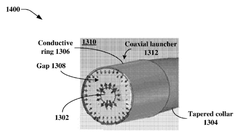
[00017] FIG. 14 is a diagram illustrating an example, non-limiting embodiment
of a
coupler in accordance with various aspects described herein.
[00018] FIG. 15 is a block diagram illustrating an example, non-limiting
embodiment
of a guided-wave communication system in accordance with various aspects
described
herein.
[00019] FIG. 16 is a block diagram illustrating an example, non-limiting
embodiment
of a transmission device in accordance with various aspects described herein.
[00020] FIG. 17 is a diagram illustrating an example, non-limiting embodiment
of an
electromagnetic distribution in accordance with various aspects described
herein.
[00021] FIG. 18 is a diagram illustrating example, non-limiting embodiments of
various electromagnetic distributions in accordance with various aspects
described
herein.
[00022] FIG. 19 is a diagram illustrating example, non-limiting embodiments of
various electromagnetic distributions in accordance with various aspects
described
herein.
[00023] FIGs. 20a and 20b are a diagram illustrating example, non-limiting
embodiments of a transmission medium in accordance with various aspects
described
herein.
[00024] FIG. 21 is a block diagram illustrating an example, non-limiting
embodiment
of a transmission device in accordance with various aspects described herein.
[00025] FIG. 22 illustrates a flow diagram of an example, non-limiting
embodiment of
a method of selecting a carrier frequency as described herein.
3
CA 02977034 2017-08-17
WO 2016/133672
PCT/US2016/015501
DETAILED DESCRIPTION
[00026] One or more embodiments are now described with reference to the
drawings,
wherein like reference numerals are used to refer to like elements throughout.
In the
following description, for purposes of explanation, numerous details are set
forth in order
to provide a thorough understanding of the various embodiments. It is evident,
however,
that the various embodiments can be practiced without these details (and
without
applying to any particular networked environment or standard).
[00027] To provide network connectivity to additional base station devices,
the
backhaul network that links the communication cells (e.g., microcells and
macrocells) to
network devices of the core network correspondingly expands. Similarly, to
provide
network connectivity to a distributed antenna system, an extended
communication system
that links base station devices and their distributed antennas is desirable. A
guided wave
communication system can be provided to enable alternative, increased or
additional
network connectivity and a waveguide coupling system can be provided to
transmit
and/or receive guided wave (e.g., surface wave) communications on a wire, such
as a
wire that operates as a single-wire transmission line (e.g., a utility line),
that operates as a
waveguide and/or that otherwise operates to guide the transmission of an
electromagnetic
wave.
[00028] In an embodiment, a waveguide coupler that is utilized in a waveguide
coupling system can be made of a dielectric material, or other low-loss
insulator (e.g.,
Teflon, polyethylene and etc.), or even be made of a conducting (e.g.,
metallic, non-
metallic, etc.) material, or any combination of the foregoing materials.
Reference
throughout the detailed description to "dielectric waveguide" is for
illustration purposes
and does not limit embodiments to being constructed solely of dielectric
materials. In
other embodiments, other dielectric or insulating materials are possible. It
will be
appreciated that a variety of transmission media can be utilized with guided
wave
communications without departing from example embodiments. Examples of such
transmission media can include one or more of the following, either alone or
in one or
more combinations: wires, whether insulated or not, and whether single-
stranded or
multi-stranded; conductors of other shapes or configurations including wire
bundles,
4
CA 02977034 2017-08-17
WO 2016/133672
PCT/US2016/015501
cables, rods, rails, pipes; non-conductors such as dielectric pipes, rods,
rails, or other
dielectric members; combinations of conductors and dielectric materials; or
other guided
wave transmission media.
[00029] One embodiment of the subject disclosure includes a coupler that
includes a
tapered collar that surrounds a transmission wire. A coaxial launcher that
surrounds the
transmission wire and guides an electromagnetic wave to the tapered collar.
The tapered
collar couples the electromagnetic wave to propagate along an outer surface of
the
transmission wire.
[00030] One embodiment of the subject disclosure includes a transmission
device that
includes a communications interface that receives a communication signal that
includes
data. A transceiver generates an electromagnetic wave based on the first
communication
signal to convey the data in accordance with at least one selected
electromagnetic (EM)
mode. A coupler is configured to receive and couple the electromagnetic wave
to a
transmission medium having an outer surface. The coupler includes a conductive
ring
and a tapered collar that surround the transmission medium. The conductive
ring guides
the electromagnetic wave to the tapered collar. The tapered collar couples the
electromagnetic wave to propagate along the outer surface of the transmission
medium
via the at least one selected EM mode.
[00031] One embodiment of the subject disclosure is directed to a method that
includes generating an electromagnetic wave to convey the data in accordance
with a
non-fundamental mode having an electromagnetic (EM) field pattern with a local
minimum at an azimuthal orientation. The method further includes coupling the
electromagnetic wave to propagate on an outer surface of a transmission medium
at a
desired orientation with respect to the transmission medium, such as a desired
orientation
that aligns with an expected orientation of water droplet formation of the
transmission
medium.
[00032] Various embodiments described herein relate to a waveguide coupling
system
for launching and extracting guided wave (e.g., surface wave communications
that are
electromagnetic waves) transmissions from a wire. At millimeter-wave
frequencies (e.g.,
30 to 300 GHz) or at lower microwave frequencies (e.g., 3 to 30 GHz), wherein
the
wavelength can be small compared to the size of the equipment, transmissions
can
CA 02977034 2017-08-17
WO 2016/133672
PCT/US2016/015501
propagate as waves guided by a waveguide, such as a strip or length of
dielectric material
or other coupler. The electromagnetic field structure of the guided wave can
be inside
and/or outside of the waveguide. When this waveguide is brought into close
proximity to
a wire (e.g., a utility line or other transmission line), at least a portion
of the guided
waves decouples from the waveguide and couples to the wire, and continues to
propagate
as guided waves, such as surface waves about the surface of the wire.
[00033] According to an example embodiment, a surface wave is a type of guided
wave that is guided by a surface of the wire, which can include an exterior or
outer
surface of the wire, or another surface of the wire that is adjacent to or
exposed to another
type of medium having different properties (e.g., dielectric properties).
Indeed, in an
example embodiment, a surface of the wire that guides a surface wave can
represent a
transitional surface between two different types of media. For example, in the
case of a
bare or uninsulated wire, the surface of the wire can be the outer or exterior
conductive
surface of the bare or uninsulated wire that is exposed to air or free space.
As another
example, in the case of insulated wire, the surface of the wire can be the
conductive
portion of the wire that meets the insulator portion of the wire, or can
otherwise be the
insulator surface of the wire that is exposed to air or free space, or can
otherwise be any
material region between the insulator surface of the wire and the conductive
portion of
the wire that meets the insulator portion of the wire, depending upon the
relative
differences in the properties (e.g., dielectric properties) of the insulator,
air, and/or the
conductor and further dependent on the frequency and propagation mode or modes
of the
guided wave.
[00034] According to an example embodiment, guided waves such as surface waves
can be contrasted with radio transmissions over free space / air or
conventional
propagation of electrical power or signals through the conductor of the wire.
Indeed.
with surface wave or guided wave systems described herein, conventional
electrical
power or signals can still propagate or be transmitted through the conductor
of the wire.
while guided waves (including surface waves and other electromagnetic waves)
can
propagate or be transmitted about the surface of the wire, according to an
example
embodiment. In an embodiment, a surface wave can have a field structure (e.g.,
an
6
CA 02977034 2017-08-17
WO 2016/133672
PCT/US2016/015501
electromagnetic field structure) that lies primarily or substantially outside
of the line,
wire, or transmission medium that serves to guide the surface wave.
[00035] According to an example embodiment, the electromagnetic waves
traveling
along the wire and around the outer surface of the wire are induced by other
electromagnetic waves traveling along a waveguide in proximity to the wire.
The
inducement of the electromagnetic waves can be independent of any electrical
potential,
charge or current that is injected or otherwise transmitted through the wires
as part of an
electrical circuit. It is to be appreciated that while a small current in the
wire may be
formed in response to the propagation of the electromagnetic wave along the
wire, this
can be due to the propagation of the electromagnetic wave along the wire
surface, and is
not formed in response to electrical potential, charge or current that is
injected into the
wire as part of an electrical circuit. The electromagnetic waves traveling on
the wire
therefore do not require a circuit to propagate along the wire surface. The
wire therefore
is a single wire transmission line that is not part of a circuit. Also, in
some embodiments,
a wire is not necessary, and the electromagnetic waves can propagate along a
single line
transmission medium that is not a wire.
[00036] According to an example embodiment, the term "about" a wire used in
conjunction with a guided wave (e.g., surface wave) can include fundamental
wave
propagation modes and other guided waves having a circular or substantially
circular
field distribution (e.g., electric field, magnetic field, electromagnetic
field, etc.) at least
partially around a wire or other transmission medium. In addition, when a
guided wave
propagates "about" a wire or other transmission medium, it can do so according
to a wave
propagation mode that includes not only the fundamental wave propagation modes
(e.g.,
zero order modes), but additionally or alternatively other non-fundamental
wave
propagation modes such as higher-order guided wave modes (e.g., 1st order
modes, 2nd
order modes, etc.), asymmetrical modes and/or other guided (e.g., surface)
waves that
have non-circular field distributions around a wire or other transmission
medium.
[00037] For example, such non-circular field distributions can be unilateral
or multi-
lateral with one or more axial lobes characterized by relatively higher field
strength
and/or one or more nulls or null regions with local minima characterized by
relatively
low-field strength, zero-field strength or substantially zero field strength.
Further, the
7
CA 02977034 2017-08-17
WO 2016/133672
PCT/US2016/015501
field distribution can otherwise vary as a function of azimuthal orientation
around the
wire such that one or more regions of azimuthal orientation around the wire
have an
electric or magnetic field strength (or combination thereof) that is higher
than one or
more other regions of azimuthal orientation, according to an example
embodiment. It
will be appreciated that the relative positions of the wave higher order modes
or
asymmetrical modes can vary as the guided wave travels along the wire.
[00038] Referring now to FIG. 1, a block diagram illustrating an example, non-
limiting embodiment of a guided-wave communication system 100 is shown. Guided-
wave communication system 100 depicts an exemplary environment in which a
transmission device, coupler or coupling module can be used.
[00039] Guided-wave communication system 100 can be a distributed antenna
system
that includes one or more base station devices (e.g., base station device 104)
that are
communicably coupled to a macrocell site 102 or other network connection. Base
station
device 104 can be connected by a wired (e.g., fiber and/or cable), or by a
wireless (e.g.,
microwave wireless) connection to macrocell site 102. Macrocells such as
macrocell site
102 can have dedicated connections to the mobile network and base station
device 104
can share and/or otherwise use macrocell site 102's connection. Base station
device 104
can be mounted on, or attached to, utility pole 116. In other embodiments,
base station
device 104 can be near transformers and/or other locations situated nearby a
power line.
[00040] Base station device 104 can facilitate connectivity to a mobile
network for
mobile devices 122 and 124. Antennas 112 and 114, mounted on or near utility
poles 118
and 120, respectively, can receive signals from base station device 104 and
transmit those
signals to mobile devices 122 and 124 over a much wider area than if the
antennas 112
and 114 were located at or near base station device 104.
[00041] It is noted
that FIG. 1 displays three utility poles, with one base station
device, for purposes of simplicity. In other embodiments, utility pole 116 can
have more
base station devices, and one or more utility poles with distributed antennas
are possible.
[00042] A transmission device, such as dielectric waveguide coupling device
106 can
transmit the signal from base station device 104 to antennas 112 and 114 via
utility or
power line(s) that connect the utility poles 116, 118, and 120. To transmit
the signal,
radio source and/or coupler 106 up converts the signal (e.g., via frequency
mixing) from
8
CA 02977034 2017-08-17
WO 2016/133672 PCT/US2016/015501
base station device 104 or otherwise converts the signal from the base station
device 104
to a microwave or millimeter-wave band signal having at least one carrier
frequency in
the microwave or millimeter-wave frequency band. The dielectric waveguide
coupling
device 106 launches a millimeter-wave band wave that propagates as a guided-
wave
(e.g., surface wave or other electromagnetic wave) traveling along the utility
line or other
wire. At utility pole 118, another transmission device, such as dielectric
waveguide
coupling device 108 that receives the guided-wave (and optionally can amplify
it as
needed or desired or operate as a digital repeater to receive it and
regenerate it) and sends
it forward as a guided-wave (e.g., surface wave or other electromagnetic wave)
on the
utility line or other wire. The dielectric waveguide coupling device 108 can
also extract a
signal from the millimeter-wave band guided-wave and shift it down in
frequency or
otherwise convert it to its original cellular band frequency (e.g., 1.9 GHz or
other defined
cellular frequency) or another cellular (or non-cellular) band frequency. An
antenna 112
can transmit (e.g., wirelessly transmit) the downshifted signal to mobile
device 122. The
process can be repeated by another transmission device, such as dielectric
waveguide
coupling device 110, antenna 114 and mobile device 124, as necessary or
desirable.
[00043] Transmissions from mobile devices 122 and 124 can also be received by
antennas 112 and 114 respectively. Repeaters on dielectric waveguide coupling
devices
108 and 110 can upshift or otherwise convert the cellular band signals to
microwave or
millimeter-wave band and transmit the signals as guided-wave (e.g., surface
wave or
other electromagnetic wave) transmissions over the power line(s) to base
station device
104.
[00044] In an example embodiment, system 100 can employ diversity paths, where
two or more utility lines or other wires are strung between the utility poles
116. 118, and
120 (e.g., for example, two or more wires between poles 116 and 120) and
redundant
transmissions from base station 104 are transmitted as guided-waves down the
surface of
the utility lines or other wires. The utility lines or other wires can be
either insulated or
uninsulated, and depending on the environmental conditions that cause
transmission
losses, the coupling devices can selectively receive signals from the
insulated or
uninsulated utility lines or other wires. The selection can be based on
measurements of
the signal-to-noise ratio of the wires, or based on determined
weather/environmental
9
CA 02977034 2017-08-17
WO 2016/133672
PCT/US2016/015501
conditions (e.g., moisture detectors, weather forecasts, etc.). The use of
diversity paths
with system 100 can enable alternate routing capabilities, load balancing,
increased load
handling, concurrent hi-directional or synchronous communications, spread
spectrum
communications, etc. (See FIG. 8 for more illustrative details).
[00045] It is noted that the use of the dielectric waveguide coupling devices
106. 108,
and 110 in FIG. 1 are by way of example only, and that in other embodiments,
other uses
are possible. For instance, dielectric waveguide coupling devices can be used
in a
backhaul communication system, providing network connectivity to base station
devices.
Dielectric waveguide coupling devices can be used in many circumstances where
it is
desirable to transmit guided-wave communications over a wire, whether
insulated or not
insulated. Dielectric waveguide coupling devices are improvements over other
coupling
devices due to no contact or limited physical and/or electrical contact with
the wires that
may carry high voltages. With dielectric waveguide coupling devices, the
apparatus can
be located away from the wire (e.g., spaced apart from the wire) and/or
located on the
wire so long as it is not electrically in contact with the wire, as the
dielectric acts as an
insulator, allowing for cheap, easy, and/or less complex installation.
However, as
previously noted conducting or non-dielectric couplers can be employed,
particularly in
configurations where the wires correspond to a telephone network, cable
television
network, broadband data service, fiber optic communications system or other
network
employing low voltages or having insulated transmission lines.
[00046] It is further noted, that while base station device 104 and macrocell
site 102
are illustrated in an example embodiment, other network configurations are
likewise
possible. For example, devices such as access points or other wireless
gateways can be
employed in a similar fashion to extend the reach of other networks such as a
wireless
local area network, a wireless personal area network or other wireless network
that
operates in accordance with a communication protocol such as a 802.11
protocol,
WINIAX protocol. Ultra Wideband protocol, Bluetooth protocol, Zigbee protocol
or other
wireless protocol.
[00047] Turning now to FIG. 2, illustrated is a block diagram of an example,
non-
limiting embodiment of a dielectric waveguide coupling system 200 in
accordance with
various aspects described herein. System 200 comprises a dielectric waveguide
204 that
CA 02977034 2017-08-17
WO 2016/133672
PCT/US2016/015501
has a wave 206 propagating as a guided-wave about a waveguide surface of the
dielectric
waveguide 204. In an example embodiment, the dielectric waveguide 204 is
curved, and
at least a portion of the dielectric waveguide 204 can be placed near a wire
202 in order
to facilitate coupling between the dielectric waveguide 204 and the wire 202,
as described
herein. The dielectric waveguide 204 can be placed such that a portion of the
curved
dielectric waveguide 204 is parallel or substantially parallel to the wire
202. The portion
of the dielectric waveguide 204 that is parallel to the wire can be an apex of
the curve, or
any point where a tangent of the curve is parallel to the wire 202. When the
dielectric
waveguide 204 is positioned or placed thusly, the wave 206 travelling along
the dielectric
waveguide 204 couples, at least in part, to the wire 202, and propagates as
guided-wave
208 around or about the wire surface of the wire 202 and longitudinally along
the wire
202. The guided-wave 208 can be characterized as a surface wave or other
electromagnetic wave, although other types of guided-waves 208 can supported
as well
without departing from example embodiments. A portion of the wave 206 that
does not
couple to the wire 202 propagates as wave 210 along the dielectric waveguide
204. It
will be appreciated that the dielectric waveguide 204 can be configured and
arranged in a
variety of positions in relation to the wire 202 to achieve a desired level of
coupling or
non-coupling of the wave 206 to the wire 202. For example, the curvature
and/or length
of the dielectric waveguide 204 that is parallel or substantially parallel, as
well as its
separation distance (which can include zero separation distance in an example
embodiment), to the wire 202 can be varied without departing from example
embodiments. Likewise, the arrangement of the dielectric waveguide 204 in
relation to
the wire 202 may be varied based upon considerations of the respective
intrinsic
characteristics (e.g., thickness, composition, electromagnetic properties.
etc.) of the wire
202 and the dielectric waveguide 204, as well as the characteristics (e.g.,
frequency.
energy level, etc.) of the waves 206 and 208.
[00048] The guided-wave 208 propagates in a direction parallel or
substantially
parallel to the wire 202, even as the wire 202 bends and flexes. Bends in the
wire 202
can increase transmission losses, which are also dependent on wire diameters,
frequency,
and materials. If the dimensions of the dielectric waveguide 204 are chosen
for efficient
power transfer, most of the power in the wave 206 is transferred to the wire
202, with
11
CA 02977034 2017-08-17
WO 2016/133672 PCT/US2016/015501
little power remaining in wave 210. It will be appreciated that the guided-
wave 208 can
still be multi-modal in nature (discussed herein), including having modes that
are non-
fundamental or asymmetric, while traveling along a path that is parallel or
substantially
parallel to the wire 202, with or without a fundamental transmission mode. In
an
example embodiment, non-fundamental or asymmetric modes can be utilized to
minimize
transmission losses and/or obtain increased propagation distances.
[00049] It is noted that the term parallel is generally a geometric construct
which often
is not exactly achievable in real systems. Accordingly, the term parallel as
utilized in the
subject disclosure represents an approximation rather than an exact
configuration when
used to describe embodiments disclosed in the subject disclosure. In an
example
embodiment, substantially parallel can include approximations that are within
30 degrees
of true parallel in all dimensions.
[00050] In an example embodiment, the wave 206 can exhibit one or more wave
propagation modes. The dielectric waveguide modes can be dependent on the
shape
and/or design of the dielectric waveguide 204. The one or more dielectric
waveguide
modes of wave 206 can generate, influence, or impact one or more wave
propagation
modes of the guided-wave 208 propagating along wire 202. In an example
embodiment,
the wave propagation modes on the wire 202 can be similar to the dielectric
waveguide
modes since both waves 206 and 208 propagate about the outside of the
dielectric
waveguide 204 and wire 202 respectively. In some embodiments, as the wave 206
couples to the wire 202, the modes can change form due to the coupling between
the
dielectric waveguide 204 and the wire 202. For example, differences in size,
material,
and/or impedances of the dielectric waveguide 204 and the wire 202 may create
additional modes not present in the dielectric waveguide modes and/or suppress
some of
the dielectric waveguide modes. The wave propagation modes can comprise the
fundamental transverse electromagnetic mode (Quasi-TEM00), where only small
electric
and/or magnetic fields extend in the direction of propagation, and the
electric and
magnetic fields extend radially outwards while the guided-wave propagates
along the
wire. This guided-wave mode can be donut shaped, where few of the
electromagnetic
fields exist within the dielectric waveguide 204 or wire 202. Waves 206 and
208 can
comprise a fundamental TEM mode where the fields extend radially outwards, and
also
12
CA 02977034 2017-08-17
WO 2016/133672
PCT/US2016/015501
comprise other, non-fundamental (e.g., asymmetric, higher-level, etc.) modes.
While
particular wave propagation modes are discussed above, other wave propagation
modes
are likewise possible such as transverse electric (TE) and transverse magnetic
(TM)
modes, based on the frequencies employed, the design of the dielectric
waveguide 204,
the dimensions and composition of the wire 202, as well as its surface
characteristics, its
optional insulation, the electromagnetic properties of the surrounding
environment, etc.
It should be noted that, depending on the frequency, the electrical and
physical
characteristics of the wire 202 and the particular wave propagation modes that
are
generated, the guided-wave 208 can travel along the conductive surface of an
oxidized
uninsulated wire, an unoxidized uninsulated wire, an insulated wire and/or
along the
insulating surface of an insulated wire.
[00051] In an example embodiment, a diameter of the dielectric waveguide 204
is
smaller than the diameter of the wire 202. For the microwave or millimeter-
band
wavelength being used, the dielectric waveguide 204 supports a single
waveguide mode
that makes up wave 206. This single waveguide mode can change as it couples to
the
wire 202 as surface wave 208. If the dielectric waveguide 204 were larger,
more than
one waveguide mode can be supported, but these additional waveguide modes may
not
couple to the wire 202 as efficiently, and higher coupling losses can result.
However, in
some alternative embodiments, the diameter of the dielectric waveguide 204 can
be equal
to or larger than the diameter of the wire 202, for example, where higher
coupling losses
are desirable or when used in conjunction with other techniques to otherwise
reduce
coupling losses (e.g., impedance matching with tapering, etc.).
[00052] In an example embodiment, the wavelength of the waves 206 and 208 are
comparable in size, or smaller than a circumference of the dielectric
waveguide 204 and
the wire 202. In an example, if the wire 202 has a diameter of 0.5 cm, and a
corresponding circumference of around 1.5 cm, the wavelength of the
transmission is
around 1.5 cm or less, corresponding to a frequency of 20 GHz or greater. In
another
embodiment, a suitable frequency of the transmission and the carrier-wave
signal is in the
range of 30 ¨ 100 GHz, perhaps around 30-60 GHz, and around 38 GHz in one
example.
In an example embodiment, when the circumference of the dielectric waveguide
204 and
wire 202 is comparable in size to, or greater, than a wavelength of the
transmission, the
13
CA 02977034 2017-08-17
WO 2016/133672
PCT/US2016/015501
waves 206 and 208 can exhibit multiple wave propagation modes including
fundamental
and/or non-fundamental (symmetric and/or asymmetric) modes that propagate over
sufficient distances to support various communication systems described
herein. The
waves 206 and 208 can therefore comprise more than one type of electric and
magnetic
field configuration. In an example embodiment, as the guided-wave 208
propagates
down the wire 202, the electrical and magnetic field configurations will
remain the same
from end to end of the wire 202. In other embodiments, as the guided-wave 208
encounters interference or loses energy due to transmission losses, the
electric and
magnetic field configurations can change as the guided-wave 208 propagates
down wire
202.
[00053] In an example embodiment, the dielectric waveguide 204 can be composed
of
nylon, Teflon, polyethylene, a polyamide, or other plastics. In other
embodiments, other
dielectric materials are possible. The wire surface of wire 202 can be
metallic with either
a bare metallic surface, or can be insulated using plastic, dielectric,
insulator or other
sheathing. In an
example embodiment, a dielectric or otherwise non-
conducting/insulated waveguide can be paired with either a bare/metallic wire
or
insulated wire. In other embodiments, a metallic and/or conductive waveguide
can be
paired with a bare/metallic wire or insulated wire. In an example embodiment,
an
oxidation layer on the bare metallic surface of the wire 202 (e.g., resulting
from exposure
of the bare metallic surface to oxygen/air) can also provide insulating or
dielectric
properties similar to those provided by some insulators or sheathings.
[00054] It is noted that the graphical representations of waves 206, 208 and
210 are
presented merely to illustrate the principles that wave 206 induces or
otherwise launches
a guided-wave 208 on a wire 202 that operates, for example, as a single wire
transmission
line. Wave 210 represents the portion of wave 206 that remains on the
dielectric
waveguide 204 after the generation of guided-wave 208. The actual electric and
magnetic fields generated as a result of such wave propagation may vary
depending on
the frequencies employed, the particular wave propagation mode or modes, the
design of
the dielectric waveguide 204, the dimensions and composition of the wire 202,
as well as
its surface characteristics, its optional insulation, the electromagnetic
properties of the
surrounding environment, etc.
14
CA 02977034 2017-08-17
WO 2016/133672
PCT/US2016/015501
[00055] It is noted that dielectric waveguide 204 can include a termination
circuit or
damper 214 at the end of the dielectric waveguide 204 that can absorb leftover
radiation
or energy from wave 210. The termination circuit or damper 214 can prevent
and/or
minimize the leftover radiation from wave 210 reflecting back toward
transmitter circuit
212. In an example embodiment, the termination circuit or damper 214 can
include
termination resistors, and/or other components that perform impedance matching
to
attenuate reflection. In some embodiments, if the coupling efficiencies are
high enough,
and/or wave 210 is sufficiently small, it may not be necessary to use a
termination circuit
or damper 214. For the sake of simplicity, these transmitter and termination
circuits or
dampers 212 and 214 are not depicted in the other figures, but in those
embodiments,
transmitter and termination circuits or dampers may possibly be used.
[00056] Further, while a single dielectric waveguide 204 is presented that
generates a
single guided-wave 208, multiple dielectric waveguides 204 placed at different
points
along the wire 202 and/or at different axial orientations about the wire can
be employed
to generate and receive multiple guided-waves 208 at the same or different
frequencies, at
the same or different phases, and/or at the same or different wave propagation
modes.
The guided-wave or waves 208 can be modulated to convey data via a modulation
technique such as phase shift keying, frequency shift keying, quadrature
amplitude
modulation, amplitude modulation, multi-carrier modulation and via multiple
access
techniques such as frequency division multiplexing, time division
multiplexing, code
division multiplexing, multiplexing via differing wave propagation modes and
via other
modulation and access strategies.
[00057] Turning now to FIG. 3, illustrated is a block diagram of an example,
non-
limiting embodiment of a dielectric waveguide coupling system 300 in
accordance with
various aspects described herein. System 300 implements a coupler that
comprises a
dielectric waveguide 304 and a wire 302 that has a wave 306 propagating as a
guided-
wave about a wire surface of the wire 302. In an example embodiment, the wave
306 can
be characterized as a surface wave or other electromagnetic wave.
[00058] In an example embodiment, the dielectric waveguide 304 is curved or
otherwise has a curvature, and can be placed near a wire 302 such that a
portion of the
curved dielectric waveguide 304 is parallel or substantially parallel to the
wire 302. The
CA 02977034 2017-08-17
WO 2016/133672 PCT/US2016/015501
portion of the dielectric waveguide 304 that is parallel to the wire can be an
apex of the
curve, or any point where a tangent of the curve is parallel to the wire 302.
When the
dielectric waveguide 304 is near the wire, the guided-wave 306 travelling
along the wire
302 can couple to the dielectric waveguide 304 and propagate as guided-wave
308 about
the dielectric waveguide 304. A portion of the guided-wave 306 that does not
couple to
the dielectric waveguide 304 propagates as guided-wave 310 (e.g., surface wave
or other
electromagnetic wave) along the wire 302.
[00059] The guided-waves 306 and 308 stay parallel to the wire 302 and
dielectric
waveguide 304, respectively, even as the wire 302 and dielectric waveguide 304
bend
and flex. Bends can increase transmission losses, which are also dependent on
wire
diameters, frequency, and materials. If the dimensions of the dielectric
waveguide 304
are chosen for efficient power transfer, most of the energy in the guided-wave
306 is
coupled to the dielectric waveguide 304 and little remains in guided-wave 310.
[00060] In an example embodiment, a receiver circuit can be placed on the end
of
dielectric waveguide 304 in order to receive wave 308. A termination circuit
can be
placed on the opposite end of the dielectric waveguide 304 in order to receive
guided-
waves traveling in the opposite direction to guided-wave 306 that couple to
the dielectric
waveguide 304. The termination circuit would thus prevent and/or minimize
reflections
being received by the receiver circuit. If the reflections are small, the
termination circuit
may not be necessary.
[00061] It is noted that the dielectric waveguide 304 can be configured such
that
selected polarizations of the surface wave 306 are coupled to the dielectric
waveguide
304 as guided-wave 308. For instance, if guided-wave 306 is made up of guided-
waves
or wave propagation modes with respective polarizations, dielectric waveguide
304 can
be configured to receive one or more guided-waves of selected polarization(s).
Guided-
wave 308 that couples to the dielectric waveguide 304 is thus the set of
guided-waves
that correspond to one or more of the selected polarization(s), and further
guided-wave
310 can comprise the guided-waves that do not match the selected
polarization(s).
[00062] The dielectric waveguide 304 can be configured to receive guided-waves
of a
particular polarization based on an angle/rotation around the wire 302 that
the dielectric
waveguide 304 is placed (the axial orientation of the coupler) and the axial
pattern of the
16
CA 02977034 2017-08-17
WO 2016/133672 PCT/US2016/015501
field structure of the guided-waves. For instance, if the coupler is oriented
to feed the
guided-waves along the horizontal access and if the guided-wave 306 is
polarized
horizontally (i.e. the filed structure of the guided-waves are concentrated on
the
horizontal axis), most of the guided-wave 306 transfers to the dielectric
waveguide as
wave 308. In another instance, if the dielectric waveguide 304 is rotated 90
degrees
around the wire 302, most of the energy from guided-wave 306 would remain
coupled to
the wire as guided-wave 310, and only a small portion would couple to the wire
302 as
wave 308.
[00063] It is noted that waves 306, 308, and 310 are shown using three
circular
symbols in FIG. 3 and in other figures in the specification. These symbols are
used to
represent a general guided-wave, but do not imply that the waves 306, 308, and
310 are
necessarily circularly polarized or otherwise circularly oriented. In fact,
waves 306, 308,
and 310 can comprise a fundamental TEM mode where the fields extend radially
outwards, and also comprise other, non-fundamental (e.g. higher-level, etc.)
modes.
These modes can be asymmetric (e.g., radial, bilateral, trilateral,
quadrilateral, etc,) in
nature as well.
[00064] It is noted also that guided-wave communications over wires can be
full
duplex, allowing simultaneous communications in both directions. Waves
traveling one
direction can pass through waves traveling in an opposite direction.
Electromagnetic
fields may cancel out at certain points and for short times due to the
superposition
principle as applied to waves. The waves traveling in opposite directions
propagate as if
the other waves weren't there, but the composite effect to an observer may be
a stationary
standing wave pattern. As the guided-waves pass through each other and are no
longer in
a state of superposition, the interference subsides. As a guided-wave (e.g.,
surface wave
or other electromagnetic wave) couples to a waveguide and moves away from the
wire.
any interference due to other guided-waves (e.g., surface waves or other
electromagnetic
waves) decreases. In an example embodiment, as guided-wave 306 (e.g., surface
wave or
other electromagnetic wave) approaches dielectric waveguide 304, another
guided-wave
(e.g., surface wave or other electromagnetic wave) (not shown) traveling from
left to
right on the wire 302 passes by causing local interference. As guided-wave 306
couples
to dielectric waveguide 304 as wave 308, and moves away from the wire 302, any
17
CA 02977034 2017-08-17
WO 2016/133672 PCT/US2016/015501
interference due to the passing guided-wave subsides.
[00065] It is noted that the graphical representations of electromagnetic
waves 306,
308 and 310 are presented merely to illustrate the principles that guided-wave
306
induces or otherwise launches a wave 308 on a dielectric waveguide 304. Guided-
wave
310 represents the portion of guided-wave 306 that remains on the wire 302
after the
generation of wave 308. The actual electric and magnetic fields generated as a
result of
such guided-wave propagation may vary depending on one or more of the shape
and/or
design of the dielectric waveguide, the relative position of the dielectric
waveguide to the
wire, the frequencies employed, the design of the dielectric waveguide 304,
the
dimensions and composition of the wire 302, as well as its surface
characteristics, its
optional insulation, the electromagnetic properties of the surrounding
environment, etc.
[00066] Turning now to FIG. 4, illustrated is a block diagram of an example,
non-
limiting embodiment of a dielectric waveguide coupling system 400 in
accordance with
various aspects described herein. System 400 implements a coupler that
comprises a
dielectric waveguide 404 that has a wave 406 propagating as a guided-wave
about a
waveguide surface of the dielectric waveguide 404. In an example embodiment,
the
dielectric waveguide 404 is curved, and an end of the dielectric waveguide 404
can be
tied, fastened, or otherwise mechanically coupled to a wire 402. When the end
of the
dielectric waveguide 404 is fastened to the wire 402, the end of the
dielectric waveguide
404 is parallel or substantially parallel to the wire 402. Alternatively,
another portion of
the dielectric waveguide beyond an end can be fastened or coupled to wire 402
such that
the fastened or coupled portion is parallel or substantially parallel to the
wire 402. The
coupling device 410 can be a nylon cable tie or other type of non-
conducting/dielectric
material that is either separate from the dielectric waveguide 404 or
constructed as an
integrated component of the dielectric waveguide 404. In other embodiments,
the
dielectric waveguide 404 can be mechanically uncoupled from the wire 402
leaving an
air gap between the coupler and the wire 402. The dielectric waveguide 404 can
be
adjacent to the wire 402 without surrounding the wire 402.
[00067] When the dielectric waveguide 404 is placed with the end parallel to
the wire
402, the guided-wave 406 travelling along the dielectric waveguide 404 couples
to the
wire 402, and propagates as guided-wave 408 about the wire surface of the wire
402. In
18
CA 02977034 2017-08-17
WO 2016/133672 PCT/US2016/015501
an example embodiment, the guided-wave 408 can be characterized as a surface
wave or
other electromagnetic wave.
[00068] It is noted that the graphical representations of waves 406 and 408
are
presented merely to illustrate the principles that wave 406 induces or
otherwise launches
a guided-wave 408 on a wire 402 that operates, for example, as a single wire
transmission
line. The actual electric and magnetic fields generated as a result of such
wave
propagation may vary depending on one or more of the shape and/or design of
the
dielectric waveguide, the relative position of the dielectric waveguide to the
wire, the
frequencies employed, the design of the dielectric waveguide 404, the
dimensions and
composition of the wire 402, as well as its surface characteristics, its
optional insulation,
the electromagnetic properties of the surrounding environment, etc.
[00069] In an example embodiment, an end of dielectric waveguide 404 can taper
towards the wire 402 in order to increase coupling efficiencies. Indeed, the
tapering of the
end of the dielectric waveguide 404 can provide impedance matching to the wire
402,
according to an example embodiment of the subject disclosure. For example, an
end of
the dielectric waveguide 404 can be gradually tapered in order to obtain a
desired level of
coupling between waves 406 and 408 as illustrated in FIG. 4.
[00070] In an example embodiment, the coupling device 410 can be placed such
that
there is a short length of the dielectric waveguide 404 between the coupling
device 410
and an end of the dielectric waveguide 404. Maximum coupling efficiencies are
realized
when the length of the end of the dielectric waveguide 404 that is beyond the
coupling
device 410 is at least several wavelengths long for whatever frequency is
being
transmitted, however shorter lengths are also possible.
[00071] Turning now to FIG. 5A, illustrated is a block diagram of an example,
non-
limiting embodiment of a dielectric waveguide coupler and transceiver system
500
(referred to herein collectively as system 500) in accordance with various
aspects
described herein. System 500 comprises a transmitter/receiver device 506 that
launches
and receives waves (e.g., guided wave 504 onto dielectric waveguide 502). The
guided
waves 504 can be used to transport signals received from and sent to a base
station 520,
mobile devices 522, or a building 524 by way of a communications interface
501. The
communications interface 501 can be an integral part of system 500.
Alternatively, the
19
CA 02977034 2017-08-17
WO 2016/133672
PCT/US2016/015501
communications interface 501 can be tethered to system 500. The communications
interface 501 can comprise a wireless interface for interfacing to the base
station 520, the
mobile devices 522, or building 524 utilizing any of various wireless
signaling protocols
(e.g., LTE, WiFi, WiMAX, IEEE 802.xx, etc.). The communications interface 501
can
also comprise a wired interface such as a fiber optic line, coaxial cable,
twisted pair, or
other suitable wired mediums for transmitting signals to the base station 520
or building
524. For embodiments where system 500 functions as a repeater, the
communications
interface 501 may not be necessary.
[00072] The output signals (e.g., Tx) of the communications interface 501 can
be
combined with a millimeter-wave carrier wave generated by a local oscillator
512 at
frequency mixer 510. Frequency mixer 510 can use heterodyning techniques or
other
frequency shifting techniques to frequency shift the output signals from
communications
interface 501. For example, signals sent to and from the communications
interface 501
can be modulated signals such as orthogonal frequency division multiplexed
(OFDM)
signals formatted in accordance with a Long-Term Evolution (LTE) wireless
protocol or
other wireless 3G, 4G, 5G or higher voice and data protocol, a Zigbee, WIMAX.
UltraWideband or IEEE 802.11 wireless protocol or other wireless protocol. In
an
example embodiment, this frequency conversion can be done in the analog
domain, and
as a result, the frequency shifting can be done without regard to the type of
communications protocol that the base station 520, mobile devices 522, or in-
building
devices 524 use. As new
communications technologies are developed, the
communications interface 501 can be upgraded or replaced and the frequency
shifting
and transmission apparatus can remain, simplifying upgrades. The carrier wave
can then
be sent to a power amplifier ("PA") 514 and can be transmitted via the
transmitter/receiver device 506 via the diplexer 516.
[00073] Signals received from the transmitter/receiver device 506 that are
directed
towards the communications interface 501 can be separated from other signals
via
diplexer 516. The transmission can then be sent to low noise amplifier ("LNA")
518 for
amplification. A frequency mixer 521, with help from local oscillator 512 can
downshift
the transmission (which is in the millimeter-wave band or around 38 GHz in
some
embodiments) to the native frequency. The communications interface 501 can
then
CA 02977034 2017-08-17
WO 2016/133672 PCT/US2016/015501
receive the transmission at an input port (Rx).
[00074] In an embodiment, transmitter/receiver device 506 can include a
cylindrical or
non-cylindrical metal (which, for example, can be hollow in an embodiment, but
not
necessarily drawn to scale) or other conducting or non-conducting waveguide
and an end
of the dielectric waveguide 502 can be placed in or in proximity to the
waveguide or the
transmitter/receiver device 506 such that when the transmitter/receiver device
506
generates a transmission, the guided wave couples to dielectric waveguide 502
and
propagates as a guided wave 504 about the waveguide surface of the dielectric
waveguide
502. In some embodiments, the guided wave 504 can propagate in part on the
outer
surface of the dielectric waveguide 502 and in part inside the dielectric
waveguide 502.
In other embodiments, the guided wave 504 can propagate substantially or
completely on
the outer surface of the dielectric waveguide 502. In yet other embodiments,
the guided
wave 504 can propagate substantially or completely inside the dielectric
waveguide 502.
In this latter embodiment, the guided wave 504 can radiate at an end of the
dielectric
waveguide 502 (such as the tapered end shown in FIG. 4) for coupling to a
transmission
medium such as a wire 402 of FIG. 4. Similarly, if guided wave 504 is incoming
(coupled
to the dielectric waveguide 502 from a wire), guided wave 504 then enters the
transmitter/receiver device 506 and couples to the cylindrical waveguide or
conducting
waveguide. While transmitter/receiver device 506 is shown to include a
separate
waveguide -- an antenna, cavity resonator, klystron, magnetron, travelling
wave tube, or
other radiating element can be employed to induce a guided wave on the
waveguide 502,
without the separate waveguide.
[00075] In an embodiment, dielectric waveguide 502 can be wholly constructed
of a
dielectric material (or another suitable insulating material), without any
metallic or
otherwise conducting materials therein. Dielectric waveguide 502 can be
composed of
nylon, Teflon, polyethylene, a polyamide, other plastics, or other materials
that are non-
conducting and suitable for facilitating transmission of electromagnetic waves
at least in
part on an outer surface of such materials. In another embodiment, dielectric
waveguide
502 can include a core that is conducting/metallic, and have an exterior
dielectric surface.
Similarly, a transmission medium that couples to the dielectric waveguide 502
for
propagating electromagnetic waves induced by the dielectric waveguide 502 or
for
21
CA 02977034 2017-08-17
WO 2016/133672
PCT/US2016/015501
supplying electromagnetic waves to the dielectric waveguide 502 can be wholly
constructed of a dielectric material (or another suitable insulating
material), without any
metallic or otherwise conducting materials therein.
[00076] It is noted that although FIG. 5A shows that the opening of
transmitter
receiver device 506 is much wider than the dielectric waveguide 502, this is
not to scale,
and that in other embodiments the width of the dielectric waveguide 502 is
comparable or
slightly smaller than the opening of the hollow waveguide. It is also not
shown, but in an
embodiment, an end of the waveguide 502 that is inserted into the
transmitter/receiver
device 506 tapers down in order to reduce reflection and increase coupling
efficiencies.
[00077] The transmitter/receiver device 506 can be communicably coupled to a
communications interface 501, and alternatively, transmitter/receiver device
506 can also
be communicably coupled to the one or more distributed antennas 112 and 114
shown in
FIG. 1. In other embodiments, transmitter/receiver device 506 can comprise
part of a
repeater system for a backhaul network.
[00078] Before
coupling to the dielectric waveguide 502, the one or more waveguide
modes of the guided wave generated by the transmitter/receiver device 506 can
couple to
the dielectric waveguide 502 to induce one or more wave propagation modes of
the
guided wave 504. The wave propagation modes of the guided wave 504 can be
different
than the hollow metal waveguide modes due to the different characteristics of
the hollow
metal waveguide and the dielectric waveguide. For instance, wave propagation
modes of
the guide wave 504 can comprise the fundamental transverse electromagnetic
mode
(Quasi-TEMoo), where only small electrical and/or magnetic fields extend in
the direction
of propagation, and the electric and magnetic fields extend radially outwards
from the
dielectric waveguide 502 while the guided waves propagate along the dielectric
waveguide 502. The fundamental transverse electromagnetic mode wave
propagation
mode may not exist inside a waveguide that is hollow. Therefore, the hollow
metal
waveguide modes that are used by transmitter/receiver device 506 are waveguide
modes
that can couple effectively and efficiently to wave propagation modes of
dielectric
waveguide 502.
[00079] It will be appreciated that other constructs or combinations of the
transmitter/receiver device 506 and dielectric waveguide 502 are possible. For
example,
22
CA 02977034 2017-08-17
WO 2016/133672
PCT/US2016/015501
a dielectric waveguide 502' can be placed tangentially or in parallel (with or
without a
gap) with respect to an outer surface of the hollow metal waveguide of the
transmitter/receiver device 506' (corresponding circuitry not shown) as
depicted by
reference 500' of FIG. 5B. In another embodiment, not shown by reference 500',
the
dielectric waveguide 502' can be placed inside the hollow metal waveguide of
the
transmitter/receiver device 506' without an axis of the dielectric waveguide
502' being
coaxially aligned with an axis of the hollow metal waveguide of the
transmitter/receiver
device 506'. In either of these embodiments, the guided wave generated by the
transmitter/receiver device 506' can couple to a surface of the dielectric
waveguide 502'
to induce one or more wave propagation modes of the guided wave 504' on the
dielectric
waveguide 502' including a fundamental mode (e.g., a symmetric mode) and/or a
non-
fundamental mode (e.g., asymmetric mode).
[00080] In one embodiment, the guided wave 504' can propagate in part on the
outer
surface of the dielectric waveguide 502' and in part inside the dielectric
waveguide 502'.
In another embodiment, the guided wave 504' can propagate substantially or
completely
on the outer surface of the dielectric waveguide 502'. In yet other
embodiments, the
guided wave 504' can propagate substantially or completely inside the
dielectric
waveguide 502'. In this latter embodiment, the guide wave 504' can radiate at
an end of
the dielectric waveguide 502' (such as the tapered end shown in FIG. 4) for
coupling to a
transmission medium such as a wire 402 of FIG. 4.
[00081] It will be further appreciated that other constructs the
transmitter/receiver
device 506 are possible. For
example, a hollow metal waveguide of a
transmitter/receiver device 506" (corresponding circuitry not shown), depicted
in FIG.
5B as reference 500", can be placed tangentially or in parallel (with or
without a gap)
with respect to an outer surface of a transmission medium such as the wire 402
of FIG. 4
without the use of the dielectric waveguide 502. In this embodiment, the
guided wave
generated by the transmitter/receiver device 506" can couple to a surface of
the wire 402
to induce one or more wave propagation modes of a guided wave 408 on the wire
402
including a fundamental mode (e.g., a symmetric mode) and/or a non-fundamental
mode
(e.g., asymmetric mode). In another embodiment, the wire 402 can be positioned
inside a
hollow metal waveguide of a transmitter/receiver device 506¨ (corresponding
circuitry
23
CA 02977034 2017-08-17
WO 2016/133672
PCT/US2016/015501
not shown) so that an axis of the wire 402 is coaxially (or not coaxially)
aligned with an
axis of the hollow metal waveguide without the use of the dielectric waveguide
502¨see
FIGs. 5B reference 500". In this embodiment, the guided wave generated by the
transmitter/receiver device 506" can couple to a surface of the wire 402 to
induce one or
more wave propagation modes of a guided wave 408 on the wire including a
fundamental
mode (e.g., a symmetric mode) and/or a non-fundamental mode (e.g., asymmetric
mode).
[00082] In the embodiments of 500" and 500'", the guided wave 408 can
propagate
in part on the outer surface of the wire 402 and in part inside the wire 402.
In another
embodiment, the guided wave 408 can propagate substantially or completely on
the outer
surface of the wire 402. The wire 402 can be a bare conductor or a conductor
with an
insulated outer surface.
[00083] Turning now to FIG. 6, illustrated is a block diagram illustrating an
example,
non-limiting embodiment of a dual dielectric waveguide coupling system 600 in
accordance with various aspects described herein. In an example embodiment, a
coupling module is shown with two or more dielectric waveguides (e.g., 604 and
606)
positioned around a wire 602 in order to receive guided-wave 608. In an
example
embodiment, the guided-wave 608 can be characterized as a surface wave or
other
electromagnetic wave. In an example embodiment, one dielectric waveguide is
enough
to receive the guided-wave 608. In that case, guided-wave 608 couples to
dielectric
waveguide 604 and propagates as guided-wave 610. If the field structure of the
guided-
wave 608 oscillates or undulates around the wire 602 due to various outside
factors, then
dielectric waveguide 606 can be placed such that guided-wave 608 couples to
dielectric
waveguide 606. In some embodiments, four or more dielectric waveguides can be
placed
around a portion of the wire 602, e.g., at 90 degrees or another spacing with
respect to
each other, in order to receive guided-waves that may oscillate or rotate
around the wire
602, that have been induced at different axial orientations or that have non-
fundamental
or higher order modes that, for example, have lobes and/or nulls or other
asymmetries
that are orientation dependent. However, it will be appreciated that there may
be less
than or more than four dielectric waveguides placed around a portion of the
wire 602
without departing from example embodiments. It will also be appreciated that
while
some example embodiments have presented a plurality of dielectric waveguides
around at
24
CA 02977034 2017-08-17
WO 2016/133672
PCT/US2016/015501
least a portion of a wire 602, this plurality of dielectric waveguides can
also be
considered as part of a single dielectric waveguide system having multiple
dielectric
waveguide subcomponents. For example, two or more dielectric waveguides can be
manufactured as single system that can be installed around a wire in a single
installation
such that the dielectric waveguides are either pre-positioned or adjustable
relative to each
other (either manually or automatically) in accordance with the single system.
Receivers
coupled to dielectric waveguides 606 and 604 can use diversity combining to
combine
signals received from both dielectric waveguides 606 and 604 in order to
maximize the
signal quality. In other embodiments, if one or the other of a dielectric
waveguide 604
and 606 receives a transmission that is above a predetermined threshold,
receivers can
use selection diversity when deciding which signal to use.
[00084] It is noted that the graphical representations of waves 608 and 610
are
presented merely to illustrate the principles that guided-wave 608 induces or
otherwise
launches a wave 610 on a dielectric waveguide 604. The actual electric and
magnetic
fields generated as a result of such wave propagation may vary depending on
the
frequencies employed, the design of the dielectric waveguide 604, the
dimensions and
composition of the wire 602, as well as its surface characteristics, its
optional insulation,
the electromagnetic properties of the surrounding environment, etc.
[00085] Turning now to FIG. 7, illustrated is a block diagram of an example,
non-
limiting embodiment of a bidirectional dielectric waveguide coupling system
700 in
accordance with various aspects described herein. Such a system 700 implements
a
transmission device with a coupling module that includes two dielectric
waveguides 704
and 714 can be placed near a wire 702 such that guided-waves (e.g., surface
waves or
other electromagnetic waves) propagating along the wire 702 are coupled to
dielectric
waveguide 704 as wave 706, and then are boosted or repeated by repeater device
710 and
launched as a guided-wave 716 onto dielectric waveguide 714. The guided-wave
716 can
then couple to wire 702 and continue to propagate along the wire 702. In an
example
embodiment, the repeater device 710 can receive at least a portion of the
power utilized
for boosting or repeating through magnetic coupling with the wire 702, which
can be a
power line.
[00086] In some embodiments, repeater device 710 can repeat the transmission
CA 02977034 2017-08-17
WO 2016/133672
PCT/US2016/015501
associated with wave 706, and in other embodiments, repeater device 710 can be
associated with a distributed antenna system and/or base station device
located near the
repeater device 710. Receiver waveguide 708 can receive the wave 706 from the
dielectric waveguide 704 and transmitter waveguide 712 can launch guided-wave
716
onto dielectric waveguide 714. Between receiver waveguide 708 and transmitter
waveguide 712, the signal can be amplified to correct for signal loss and
other
inefficiencies associated with guided-wave communications or the signal can be
received
and processed to extract the data contained therein and regenerated for
transmission. In
an example embodiment, a signal can be extracted from the transmission and
processed
and otherwise emitted to mobile devices nearby via distributed antennas
communicably
coupled to the repeater device 710. Similarly, signals and/or communications
received
by the distributed antennas can be inserted into the transmission that is
generated and
launched onto dielectric waveguide 714 by transmitter waveguide 712.
Accordingly, the
repeater system 700 depicted in FIG. 7 can be comparable in function to the
dielectric
waveguide coupling device 108 and 110 in FIG. 1.
[00087] It is noted that although FIG. 7 shows guided-wave transmissions 706
and
716 entering from the left and exiting to the right respectively, this is
merely a
simplification and is not intended to be limiting. In other embodiments,
receiver
waveguide 708 and transmitter waveguide 712 can also function as transmitters
and
receivers respectively, allowing the repeater device 710 to be bi-directional.
[00088] In an example embodiment, repeater device 710 can be placed at
locations
where there are discontinuities or obstacles on the wire 702. These obstacles
can include
transformers, connections, utility poles, and other such power line devices.
The repeater
device 710 can help the guided (e.g., surface) waves jump over these obstacles
on the line
and boost the transmission power at the same time. In other embodiments, a
dielectric
waveguide can be used to jump over the obstacle without the use of a repeater
device. In
that embodiment, both ends of the dielectric waveguide can be tied or fastened
to the
wire, thus providing a path for the guided-wave to travel without being
blocked by the
obstacle.
[00089] Turning now to FIG. 8, illustrated is a block diagram of an example,
non-
limiting embodiment of a bidirectional dielectric waveguide coupler 800 in
accordance
26
CA 02977034 2017-08-17
WO 2016/133672
PCT/US2016/015501
with various aspects described herein. The bidirectional dielectric waveguide
coupler
800 implements a transmission device with a coupling module that can employ
diversity
paths in the case of when two or more wires are strung between utility poles.
Since
guided-wave transmissions have different transmission efficiencies and
coupling
efficiencies for insulated wires and un-insulated wires based on weather,
precipitation
and atmospheric conditions, it can be advantageous to selectively transmit on
either an
insulated wire or un-insulated wire at certain times.
[00090] In the embodiment shown in FIG. 8, the repeater device uses a receiver
waveguide 808 to receive a guided-wave traveling along uninsulated wire 802
and
repeats the transmission using transmitter waveguide 810 as a guided-wave
along
insulated wire 804. In other embodiments, repeater device can switch from the
insulated
wire 804 to the un-insulated wire 802, or can repeat the transmissions along
the same
paths. Repeater device 806 can include sensors, or be in communication with
sensors
that indicate conditions that can affect the transmission. Based on the
feedback received
from the sensors, the repeater device 806 can make the determination about
whether to
keep the transmission along the same wire, or transfer the transmission to the
other wire.
[00091] Turning now to FIG. 9, illustrated is a block diagram illustrating an
example,
non-limiting embodiment of a bidirectional repeater system 900. Bidirectional
repeater
system 900 implements a transmission device with a coupling module that
includes
waveguide coupling devices 902 and 904 that receive and transmit transmissions
from
other coupling devices located in a distributed antenna system or backhaul
system.
[00092] In various embodiments, waveguide coupling device 902 can receive a
transmission from another waveguide coupling device, wherein the transmission
has a
plurality of subcarriers. Diplexer 906 can separate the transmission from
other
transmissions. for example by filtration, and direct the transmission to low-
noise
amplifier ("LNA") 908. A frequency mixer 928, with help from a local
oscillator 912,
can downshift the transmission (which is in the millimeter-wave band or around
38 GHz
in some embodiments) to a lower frequency, whether it is a cellular band (-1.9
GHz) for
a distributed antenna system, a native frequency, or other frequency for a
backhaul
system. An extractor 932 can extract the signal on the subcarrier that
corresponds to the
antenna or other output component 922 and direct the signal to the output
component
27
CA 02977034 2017-08-17
WO 2016/133672 PCT/US2016/015501
922. For the signals that are not being extracted at this antenna location,
extractor 932
can redirect them to another frequency mixer 936, where the signals are used
to modulate
a carrier wave generated by local oscillator 914. The carrier wave, with its
subcarriers, is
directed to a power amplifier ("PA") 916 and is retransmitted by waveguide
coupling
device 904 to another repeater system, via diplexer 920.
[00093] At the output device 922. a PA 924 can boost the signal for
transmission to the
mobile device. An LNA 926 can be used to amplify weak signals that are
received from
the mobile device and then send the signal to a multiplexer 934 which merges
the signal
with signals that have been received from waveguide coupling device 904. The
output
device 922 can be coupled to an antenna in a distributed antenna system or
other antenna
via, for example, a diplexer, duplexer or a transmit receive switch not
specifically shown.
The signals received from coupling device 904 have been split by diplexer 920,
and then
passed through LNA 918, and downshifted in frequency by frequency mixer 938.
When
the signals are combined by multiplexer 934, they are upshifted in frequency
by
frequency mixer 930, and then boosted by PA 910, and transmitted back to the
launcher
or on to another repeater by waveguide coupling device 902. In an example
embodiment,
the bidirectional repeater system 900 can be just a repeater without the
antenna/output
device 922. It will be appreciated that in some embodiments, a bidirectional
repeater
system 900 could also be implemented using two distinct and separate uni-
directional
repeaters. In an alternative embodiment, a bidirectional repeater system 900
could also
be a booster or otherwise perform retransmissions without downshifting and
upshifting.
Indeed in example embodiment, the retransmissions can be based upon receiving
a signal
or guided-wave and performing some signal or guided-wave processing or
reshaping,
filtering, and/or amplification, prior to retransmission of the signal or
guided-wave.
[00094] FIG. 10 illustrates a process in connection with the aforementioned
systems.
The process in FIG. 10 can be implemented for example by systems 100, 200,
300. 400,
500, 600, 700, 800, and 900 illustrated in FIGs. 1-9 respectively. While for
purposes of
simplicity of explanation, the methods are shown and described as a series of
blocks, it is
to be understood and appreciated that the claimed subject matter is not
limited by the
order of the blocks, as some blocks may occur in different orders and/or
concurrently
28
CA 02977034 2017-08-17
WO 2016/133672
PCT/US2016/015501
with other blocks from what is depicted and described herein. Moreover, not
all
illustrated blocks may be required to implement the methods described
hereinafter.
[00095] FIG. 10 illustrates a flow diagram of an example, non-limiting
embodiment of
a method for transmitting a transmission with a dielectric waveguide coupler
as described
herein. Method 1000 can begin at 1002 where a first electromagnetic wave is
emitted by
a transmission device that propagates at least in part on a waveguide surface
of a
waveguide, wherein the waveguide surface of the waveguide does not surround in
whole
or in substantial part a wire surface of a wire. The transmission that is
generated by a
transmitter can be based on a signal received from a base station device,
access point,
network or a mobile device.
[00096] At 1004, based upon configuring the waveguide in proximity of the
wire, the
guided-wave then couples at least a part of the first electromagnetic wave to
a wire
surface, forming a second electromagnetic wave (e.g., a surface wave) that
propagates at
least partially around the wire surface, wherein the wire is in proximity to
the waveguide.
This can be done in response to positioning a portion of the dielectric
waveguide (e.g., a
tangent of a curve of the dielectric waveguide) near and parallel to the wire,
wherein a
wavelength of the electromagnetic wave is smaller than a circumference of the
wire and
the dielectric waveguide. The guided-wave, or surface wave, stays parallel to
the wire
even as the wire bends and flexes. Bends can increase transmission losses,
which are
also dependent on wire diameters, frequency, and materials. The coupling
interface
between the wire and the waveguide can also be configured to achieve the
desired level
of coupling, as described herein, which can include tapering an end of the
waveguide to
improve impedance matching between the waveguide and the wire.
[00097] The transmission that is emitted by the transmitter can exhibit one or
more
waveguide modes. The waveguide modes can be dependent on the shape and/or
design
of the waveguide. The propagation modes on the wire can be different than the
waveguide modes due to the different characteristics of the waveguide and the
wire.
When the circumference of the wire is comparable in size to, or greater, than
a
wavelength of the transmission, the guided-wave exhibits multiple wave
propagation
modes. The guided-wave can therefore comprise more than one type of electric
and
magnetic field configuration. As the guided-wave (e.g., surface wave)
propagates down
29
CA 02977034 2017-08-17
WO 2016/133672
PCT/US2016/015501
the wire, the electrical and magnetic field configurations may remain
substantially the
same from end to end of the wire or vary as the transmission traverses the
wave by
rotation, dispersion, attenuation or other effects.
[00098] Referring now to FIG. 11, there is illustrated a block diagram of a
computing
environment in accordance with various aspects described herein. In order to
provide
additional context for various embodiments of the embodiments described
herein, FIG.
11 and the following discussion are intended to provide a brief, general
description of a
suitable computing environment 1100 in which the various embodiments of the
embodiment described herein can be implemented. While the embodiments have
been
described above in the general context of computer-executable instructions
that can be
run on one or more computers, those skilled in the art will recognize that the
embodiments can be also implemented in combination with other program modules
and/or as a combination of hardware and software.
[00099] Generally, program modules comprise routines, programs, components,
data
structures, etc., that perform particular tasks or implement particular
abstract data types.
Moreover, those skilled in the art will appreciate that the inventive methods
can be
practiced with other computer system configurations, comprising single-
processor or
multiprocessor computer systems, minicomputers, mainframe computers, as well
as
personal computers, hand-held computing devices, microprocessor-based or
programmable consumer electronics, and the like, each of which can be
operatively
coupled to one or more associated devices.
[000100] The terms "first," "second," "third," and so forth, unless otherwise
clear by
context, is for clarity only and doesn't otherwise indicate or imply any order
in time. For
instance, "a first determination," "a second determination," and "a third
determination,"
does not indicate or imply that the first determination is to be made before
the second
determination, or vice versa, etc.
[000101] The illustrated embodiments of the embodiments herein can be also
practiced
in distributed computing environments where certain tasks are performed by
remote
processing devices that are linked through a communications network. In a
distributed
computing environment, program modules can be located in both local and remote
memory storage devices.
CA 02977034 2017-08-17
WO 2016/133672 PCT/US2016/015501
[000102] Computing devices typically comprise a variety of media, which can
comprise
computer-readable storage media and/or communications media, which two terms
are
used herein differently from one another as follows. Computer-readable storage
media
can be any available storage media that can be accessed by the computer and
comprises
both volatile and nonvolatile media, removable and non-removable media. By way
of
example, and not limitation, computer-readable storage media can be
implemented in
connection with any method or technology for storage of information such as
computer-
readable instructions, program modules, structured data or unstructured data.
[000103] Computer-readable storage media can comprise, but are not limited to,
random access memory (RAM), read only memory (ROM), electrically erasable
programmable read only memory (EEPROM), flash memory or other memory
technology, compact disk read only memory (CD-ROM), digital versatile disk
(DVD) or
other optical disk storage, magnetic cassettes, magnetic tape, magnetic disk
storage or
other magnetic storage devices or other tangible and/or non-transitory media
which can
be used to store desired information. In this regard, the terms "tangible" or
"non-
transitory" herein as applied to storage, memory or computer-readable media,
are to be
understood to exclude only propagating transitory signals per se as modifiers
and do not
relinquish rights to all standard storage, memory or computer-readable media
that are not
only propagating transitory signals per se.
[000104] Computer-readable storage media can be accessed by one or more local
or
remote computing devices, e.g., via access requests, queries or other data
retrieval
protocols, for a variety of operations with respect to the information stored
by the
medium.
[000105] Communications media typically embody computer-readable instructions.
data structures, program modules or other structured or unstructured data in a
data signal
such as a modulated data signal, e.g., a carrier wave or other transport
mechanism, and
comprise any information delivery or transport media. The term "modulated data
signal"
or signals refers to a signal that has one or more of its characteristics set
or changed in
such a manner as to encode information in one or more signals. By way of
example, and
not limitation, communication media comprises wired media, such as a wired
network or
31
CA 02977034 2017-08-17
WO 2016/133672
PCT/US2016/015501
direct-wired connection, and wireless media such as acoustic, RF, infrared and
other
wireless media.
[000106] With reference again to FIG. 11, the example environment 1100 for
transmitting and receiving signals via base station (e.g., base station
devices 104 and 508)
and repeater devices (e.g., repeater devices 710, 806, and 900) comprises a
computer
1102, the computer 1102 comprising a processing unit 1104, a system memory
1106 and
a system bus 1108. The system bus 1108 couples system components including,
but not
limited to, the system memory 1106 to the processing unit 1104. The processing
unit
1104 can be any of various commercially available processors. Dual
microprocessors
and other multi-processor architectures can also be employed as the processing
unit 1104.
[000107] The system bus 1108 can be any of several types of bus structure that
can
further interconnect to a memory bus (with or without a memory controller), a
peripheral
bus, and a local bus using any of a variety of commercially available bus
architectures.
The system memory 1106 comprises ROM 1110 and RAM 1112. A basic input/output
system (BIOS) can be stored in a non-volatile memory such as ROM, erasable
programmable read only memory (EPROM), EEPROM, in which the BIOS contains the
basic routines that help to transfer information between elements within the
computer
1102, such as during startup. The RAM 1112 can also comprise a high-speed RAM
such
as static RAM for caching data.
[000108] The computer 1102 further comprises an internal hard disk drive (HDD)
1114
(e.g., EIDE, SATA), which internal hard disk drive 1114 can also be configured
for
external use in a suitable chassis (not shown), a magnetic floppy disk drive
(FDD) 1116.
(e.g., to read from or write to a removable diskette 1118) and an optical disk
drive 1120,
(e.g., reading a CD-ROM disk 1122 or, to read from or write to other high
capacity
optical media such as the DVD). The hard disk drive 1114, magnetic disk drive
1116 and
optical disk drive 1120 can be connected to the system bus 1108 by a hard disk
drive
interface 1124, a magnetic disk drive interface 1126 and an optical drive
interface 1128.
respectively. The interface for external drive implementations comprises at
least one or
both of Universal Serial Bus (USB) and Institute of Electrical and Electronics
Engineers
(IEEE) 1394 interface technologies. Other external drive connection
technologies are
within contemplation of the embodiments described herein.
32
CA 02977034 2017-08-17
WO 2016/133672 PCT/US2016/015501
[000109] The drives and their associated computer-readable storage media
provide
nonvolatile storage of data, data structures, computer-executable
instructions, and so
forth. For the computer 1102, the drives and storage media accommodate the
storage of
any data in a suitable digital format. Although the description of computer-
readable
storage media above refers to a hard disk drive (HDD), a removable magnetic
diskette,
and a removable optical media such as a CD or DVD, it should be appreciated by
those
skilled in the art that other types of storage media which are readable by a
computer, such
as zip drives, magnetic cassettes, flash memory cards, cartridges, and the
like, can also be
used in the example operating environment, and further, that any such storage
media can
contain computer-executable instructions for performing the methods described
herein.
[000110] A number of program modules can be stored in the drives and RAM 1112,
comprising an operating system 1130, one or more application programs 1132,
other
program modules 1134 and program data 1136. All or portions of the operating
system,
applications, modules, and/or data can also be cached in the RAM 1112. The
systems
and methods described herein can be implemented utilizing various commercially
available operating systems or combinations of operating systems. Examples of
application programs 1132 that can be implemented and otherwise executed by
processing unit 1104 include the diversity selection determining performed by
repeater
device 806. Base station device 508 shown in FIG. 5, also has stored in memory
many
applications and programs that can be executed by processing unit 1104 in this
exemplary
computing environment 1100.
[000111] A user can enter commands and information into the computer 1102
through
one or more wired/wireless input devices, e.g., a keyboard 1138 and a pointing
device,
such as a mouse 1140. Other input devices (not shown) can comprise a
microphone, an
infrared (lR) remote control, a joystick, a game pad, a stylus pen, touch
screen or the like.
These and other input devices are often connected to the processing unit 1104
through an
input device interface 1142 that can be coupled to the system bus 1108, but
can be
connected by other interfaces, such as a parallel port. an IEEE 1394 serial
port, a game
port, a universal serial bus (USB) port, an IR interface, etc.
[000112] A monitor 1144 or other type of display device can be also connected
to the
system bus 1108 via an interface, such as a video adapter 1146. It will also
be
33
CA 02977034 2017-08-17
WO 2016/133672 PCT/US2016/015501
appreciated that in alternative embodiments, a monitor 1144 can also be any
display
device (e.g., another computer having a display, a smart phone, a tablet
computer, etc.)
for receiving display information associated with computer 1102 via any
communication
means, including via the Internet and cloud-based networks. In addition to the
monitor
1144, a computer typically comprises other peripheral output devices (not
shown), such
as speakers, printers, etc.
[000113] The computer 1102 can operate in a networked environment using
logical
connections via wired and/or wireless communications to one or more remote
computers,
such as a remote computer(s) 1148. The remote computer(s) 1148 can be a
workstation.
a server computer, a router, a personal computer, portable computer,
microprocessor-
based entertainment appliance, a peer device or other common network node, and
typically comprises many or all of the elements described relative to the
computer 1102,
although, for purposes of brevity, only a memory/storage device 1150 is
illustrated. The
logical connections depicted comprise wired/wireless connectivity to a local
area network
(LAN) 1152 and/or larger networks, e.g., a wide area network (WAN) 1154. Such
LAN
and WAN networking environments are commonplace in offices and companies, and
facilitate enterprise-wide computer networks, such as intranets, all of which
can connect
to a global communications network, e.g., the Internet.
[000114] When used in a LAN networking environment, the computer 1102 can be
connected to the local network 1152 through a wired and/or wireless
communication
network interface or adapter 1156. The adapter 1156 can facilitate wired or
wireless
communication to the LAN 1152, which can also comprise a wireless AP disposed
thereon for communicating with the wireless adapter 1156.
[000115] When used in a WAN networking environment, the computer 1102 can
comprise a modem 1158 or can be connected to a communications server on the
WAN
1154 or has other means for establishing communications over the WAN 1154,
such as
by way of the Internet. The modem 1158, which can be internal or external and
a wired
or wireless device, can be connected to the system bus 1108 via the input
device interface
1142. In a networked environment, program modules depicted relative to the
computer
1102 or portions thereof, can be stored in the remote memory/storage device
1150. It
34
CA 02977034 2017-08-17
WO 2016/133672 PCT/US2016/015501
will be appreciated that the network connections shown are example and other
means of
establishing a communications link between the computers can be used.
[000116] The computer 1102 can be operable to communicate with any wireless
devices or entities operatively disposed in wireless communication, e.g., a
printer,
scanner, desktop and/or portable computer, portable data assistant,
communications
satellite, any piece of equipment or location associated with a wirelessly
detectable tag
(e.g., a kiosk, news stand, restroom), and telephone. This can comprise
Wireless Fidelity
(Wi-Fi) and BLUETOOTH wireless technologies. Thus, the communication can be a
predefined structure as with a conventional network or simply an ad hoc
communication
between at least two devices.
[000117] Wi-Fi can allow connection to the Internet from a couch at home, a
bed in a
hotel room or a conference room at work, without wires. Wi-Fi is a wireless
technology
similar to that used in a cell phone that enables such devices, e.g.,
computers, to send and
receive data indoors and out; anywhere within the range of a base station. Wi-
Fi
networks use radio technologies called IEEE 802.11 (a, b, g, n, ac, etc.) to
provide secure,
reliable, fast wireless connectivity. A Wi-Fi network can be used to connect
computers
to each other, to the Internet, and to wired networks (which can use IEEE
802.3 or
Ethernet). Wi-Fi networks operate in the unlicensed 2.4 and 5 GHz radio bands
for
example or with products that contain both bands (dual band), so the networks
can
provide real-world performance similar to the basic 10BaseT wired Ethernet
networks
used in many offices.
[000118] FIG. 12 presents an example embodiment 1200 of a mobile network
platform
1210 that can implement and exploit one or more aspects of the disclosed
subject matter
described herein. In one or more embodiments, the mobile network platform 1210
can
generate and receive signals transmitted and received by base stations (e.g.,
base station
devices 104 and 508) and repeater devices (e.g., repeater devices 710, 806.
and 900)
associated with the disclosed subject matter. Generally, wireless network
platform 1210
can comprise components, e.g., nodes, gateways, interfaces, servers, or
disparate
platforms, that facilitate both packet-switched (PS) (e.g., internet protocol
(IP), frame
relay, asynchronous transfer mode (ATM)) and circuit-switched (CS) traffic
(e.g., voice
and data), as well as control generation for networked wireless
telecommunication. As a
CA 02977034 2017-08-17
WO 2016/133672 PCT/US2016/015501
non-limiting example, wireless network platform 1210 can be included in
telecommunications carrier networks, and can be considered carrier-side
components as
discussed elsewhere herein. Mobile network platform 1210 comprises CS gateway
node(s) 1212 which can interface CS traffic received from legacy networks like
telephony network(s) 1240 (e.g., public switched telephone network (PSTN), or
public
land mobile network (PLMN)) or a signaling system #7 (S57) network 1260.
Circuit
switched gateway node(s) 1212 can authorize and authenticate traffic (e.g.,
voice) arising
from such networks. Additionally. CS gateway node(s) 1212 can access mobility,
or
roaming, data generated through S57 network 1260; for instance, mobility data
stored in
a visited location register (VLR), which can reside in memory 1230. Moreover,
CS
gateway node(s) 1212 interfaces CS-based traffic and signaling and PS gateway
node(s)
1218. As an example, in a 3GPP UMTS network, CS gateway node(s) 1212 can be
realized at least in part in gateway GPRS support node(s) (GGSN). It should be
appreciated that functionality and specific operation of CS gateway node(s)
1212, PS
gateway node(s) 1218, and serving node(s) 1216, is provided and dictated by
radio
technology(ies) utilized by mobile network platform 1210 for
telecommunication.
[000119] In addition to receiving and processing CS-switched traffic and
signaling, PS
gateway node(s) 1218 can authorize and authenticate PS-based data sessions
with served
mobile devices. Data sessions can comprise traffic, or content(s), exchanged
with
networks external to the wireless network platform 1210, like wide area
network(s)
(WANs) 1250, enterprise network(s) 1270, and service network(s) 1280, which
can be
embodied in local area network(s) (LANs). can also be interfaced with mobile
network
platform 1210 through PS gateway node(s) 1218. It is to be noted that WANs
1250 and
enterprise network(s) 1270 can embody, at least in part, a service network(s)
like IP
multimedia subsystem (IMS). Based on radio technology layer(s) available in
technology
resource(s), packet-switched gateway node(s) 1218 can generate packet data
protocol
contexts when a data session is established; other data structures that
facilitate routing of
packetized data also can be generated. To that end, in an aspect, PS gateway
node(s)
1218 can comprise a tunnel interface (e.g., tunnel termination gateway (TTG)
in 3GPP
UMTS network(s) (not shown)) which can facilitate packetized communication
with
disparate wireless network(s), such as Wi-Fi networks.
36
CA 02977034 2017-08-17
WO 2016/133672
PCT/US2016/015501
[000120] In embodiment 1200, wireless network platform 1210 also comprises
serving
node(s) 1216 that, based upon available radio technology layer(s) within
technology
resource(s). convey the various packetized flows of data streams received
through PS
gateway node(s) 1218. It is to be noted that for technology resource(s) that
rely primarily
on CS communication, server node(s) can deliver traffic without reliance on PS
gateway
node(s) 1218; for example, server node(s) can embody at least in part a mobile
switching
center. As an example, in a 3GPP UMTS network, serving node(s) 1216 can be
embodied in serving GPRS support node(s) (SGSN).
[000121] For radio technologies that exploit packetized communication,
server(s) 1214
in wireless network platform 1210 can execute numerous applications that can
generate
multiple disparate packetized data streams or flows, and manage (e.g.,
schedule, queue,
format...) such flows. Such application(s) can comprise add-on features to
standard
services (for example, provisioning, billing, customer support...) provided by
wireless
network platform 1210. Data streams (e.g., content(s) that are part of a voice
call or data
session) can be conveyed to PS gateway node(s) 1218 for
authorization/authentication
and initiation of a data session, and to serving node(s) 1216 for
communication
thereafter. In addition to application server, server(s) 1214 can comprise
utility server(s),
a utility server can comprise a provisioning server, an operations and
maintenance server,
a security server that can implement at least in part a certificate authority
and firewalls as
well as other security mechanisms, and the like. In an aspect, security
server(s) secure
communication served through wireless network platform 1210 to ensure
network's
operation and data integrity in addition to authorization and authentication
procedures
that CS gateway node(s) 1212 and PS gateway node(s) 1218 can enact. Moreover,
provisioning server(s) can provision services from external network(s) like
networks
operated by a disparate service provider; for instance, WAN 1250 or Global
Positioning
System (GPS) network(s) (not shown). Provisioning server(s) can also provision
coverage through networks associated to wireless network platform 1210 (e.g.,
deployed
and operated by the same service provider), such as the distributed antennas
networks
shown in FIG. 1(s) that enhance wireless service coverage by providing more
network
coverage. Repeater devices such as those shown in FIGs 7. 8, and 9 also
improve
network coverage in order to enhance subscriber service experience by way of
UE 1275.
37
CA 02977034 2017-08-17
WO 2016/133672
PCT/US2016/015501
[000122] It is to be noted that server(s) 1214 can comprise one or more
processors
configured to confer at least in part the functionality of macro network
platform 1210.
To that end, the one or more processor can execute code instructions stored in
memory
1230, for example. It is should be appreciated that server(s) 1214 can
comprise a content
manager, which operates in substantially the same manner as described
hereinbefore.
[000123] In example embodiment 1200, memory 1230 can store information related
to
operation of wireless network platform 1210. Other operational information can
comprise provisioning information of mobile devices served through wireless
platform
network 1210, subscriber databases; application intelligence, pricing schemes,
e.g.,
promotional rates, flat-rate programs, couponing campaigns; technical
specification(s)
consistent with telecommunication protocols for operation of disparate radio,
or wireless,
technology layers; and so forth. Memory 1230 can also store information from
at least
one of telephony network(s) 1240, WAN 1250, enterprise network(s) 1270, or SS7
network 1260. In an aspect, memory 1230 can be, for example, accessed as part
of a data
store component or as a remotely connected memory store.
[000124] In order to provide a context for the various aspects of the
disclosed subject
matter, FIG. 12, and the following discussion, are intended to provide a
brief, general
description of a suitable environment in which the various aspects of the
disclosed
subject matter can be implemented. While the subject matter has been described
above in
the general context of computer-executable instructions of a computer program
that runs
on a computer and/or computers, those skilled in the art will recognize that
the disclosed
subject matter also can be implemented in combination with other program
modules.
Generally, program modules comprise routines, programs, components, data
structures,
etc. that perform particular tasks and/or implement particular abstract data
types.
[000125] Turning now to FIG. 13 a diagram is presented illustrating an
example, non-
limiting embodiment of a coupler in accordance with various aspects described
herein. In
particular, a diagram 1300 is presented of a coupler 1310 that is implemented
as part of a
transmission device for launching electromagnetic waves on an outer surface of
a
transmission medium, such as the insulated medium voltage wire 1302 that is
shown.
The coupler 1310 includes a tapered collar 1304 that surrounds the insulated
medium
voltage wire 1302 (it being appreciated however, that other conductive wires
can be
38
CA 02977034 2017-08-17
WO 2016/133672 PCT/US2016/015501
utilized as well). The tapered collar 1304 can be constructed of a dielectric
or other non-
conductive material. A conductive ring 1306 also surrounds the insulated
medium
voltage wire 1302 in whole, substantially or in part, creating a gap 1308 such
as an air
gap or other gap (whether filled with a portion of the tapered collar 1304,
other dielectric
material or not) between the conductive ring 1306 and the insulated medium
voltage wire
1302 to form a coaxial launcher 1312. For example, the conductive ring 1306
can be
filled or substantially filled with a dielectric material that merges with the
larger diameter
end of the tapered collar 1304 that is constructed of the same dielectric
material. In this
fashion, the dielectric material inside the conductive ring 1306 and the
dielectric material
forming the tapered collar 1304 can be constructed of a single dielectric
element. The
conductive ring 1306 can be constructed of a metallic ring, a metal coated
ring or other
conductive material.
[000126] In operation, the coupler 1310 receives, at an open end of the
conductive ring
1306 or other structure of the coaxial launcher 1312 that couples to a
transmitter or
transceiver to launch an electromagnetic wave from a transmitter or
transceiver as part of
a transmission device and guide the electromagnetic wave to the tapered collar
1304.
The tapered collar 1304 couples the electromagnetic wave to propagate along an
outer
surface of the insulated medium voltage wire 1302. While the conductive ring
1306 is
shown as being non-tapered and having a particular shape, in other examples
the
conductive ring can be tapered. Further while the conductive ring 1306 and
tapered
collar 1304 are shown as having a circular outer perimeter, shapes such as
ellipsoid
shapes, polygonal shapes or other shapes could likewise be employed. The
coupler 1310
can be installed on the MV wire 1302 via a splicing device that is configured
with the
tapered ends described above. Alternatively, the coupler 1310 can be
constructed in a
clamshell configuration with two or more pieces that are joined together to
surround the
MV wire 1302, can be constructed of a flexible material and have a slotted
bottom that
can be opened and wrapped around the MV wire 1302 for ease of installation or
can be
configured for installation in other ways.
[000127] Turning now to FIG. 14 a diagram is presented illustrating an
example, non-
limiting embodiment of a coupler in accordance with various aspects described
herein. In
particular, in diagram 1400, the coupler 1310 from FIG. 13 is shown again in
greater
39
CA 02977034 2017-08-17
WO 2016/133672 PCT/US2016/015501
detail. As shown, the coupler 1310 is coaxially aligned with the insulated
medium
voltage wire 1302. The conductive ring 1306 (with optional dielectric material
in the gap
between the metallic ring and the MV wire 1302) serves as a coaxial launcher
1312 to
receive and/or guide an electromagnetic wave with a selected EM mode structure
(such
as a TEM mode, TE mode or TM mode). This selected EM mode structure can be
fundamental mode only, can include only one or more non-fundamental modes, or
a
combination of the fundamental mode and one or more non-fundamental modes. The
tapered collar 1304 preserves the mode structure between the coaxial launcher
1312 and
the insulated medium voltage wire 1302, so as to launch the electromagnetic
wave on the
outer surface of the insulated medium voltage wire 1302 with the selected mode
structure.
[000128] By selectively launching a desired EM wave mode, the coupler 1310 can
be
used to launch EM waves in a modal "sweet spot" that enhances electromagnetic
wave
propagation along an insulated transmission medium and reduces end-to-end
transmission loss. In this particular mode, EM waves are partially embedded in
the
insulator and partially travelling on the outer surface of the insulator. In
this fashion, EM
waves are "lightly coupled to the insulator so as to enable EM wave
propagation at long
distances with low propagation loss. Further details regarding this
propagation mode,
including several optional functions and features, will be discussed in
conjunction with
FIGs. 17-19.
[000129] In a further example, by selectively launching a desired EM wave
mode, the
coupler 1310 can be used to launch EM waves that mitigate or circumvent the
effects of
water droplets. In particular an EM wave mode can be selected to have a local
minimum
(or null) at the orientation of expected rain droplet formation while the
majority of the
electromagnetic energy is oriented in the dry (or dryer) spots on the
insulated line.
Further details regarding this example. including several optional functions
and features,
will be discussed in conjunction with FIGs. 20a and 20b.
[000130] While the coupler 1310 is shown for use with the insulated medium
voltage
wire 1302, such a coupler could also be used in conjunction with other
transmission
mediums including other transmission wires, other single wire transmission
systems and
other transmission mediums without wires. In particular, while FIGs. 13 and 14
show an
CA 02977034 2017-08-17
WO 2016/133672 PCT/US2016/015501
insulated medium voltage wire 1302 having a circular shape and coupler 1310
having a
corresponding circular shape, this is not meant to be limiting. In other
embodiments,
wires and couplers can have a variety of shapes, sizes, and configurations.
The shapes
can include, but not be limited to: ovals or other ellipsoid shapes, octagons,
quadrilaterals
or other polygons with either sharp or rounded edges, or other shapes.
Additionally, in
some embodiments, the transmission medium can include stranded wires
comprising
smaller gauge wires, such as a helical strand, braid, bundle or other coupling
of
individual strands into a single wire or wire bundle.
[000131] Turning now to FIG. 15, a block diagram is shown illustrating an
example,
non-limiting embodiment of a guided-wave communication system 1550. In
operation, a
transmission device 1500 receives one or more communication signals 1510 from
a
communication network or other communications device that includes data and
generates
guided waves 1520 to convey the data via the transmission medium 1525 to the
transmission device 1502. The transmission device 1502 receives the guided
waves 1520
and converts them to communication signals 1512 that include the data for
transmission
to a communications network or other communications device. The communication
network or networks can include a wireless communication network such as a
mobile
data network, a cellular voice and data network, a wireless local area network
(e.g., WiFi
or an 802.xx network), a satellite communications network, a personal area
network or
other wireless network. The communication network or networks can include a
wired
communication network such as a telephone network, an Ethernet network, a
local area
network, a wide area network such as the Internet, a broadband access network,
a cable
network, a fiber optic network, or other wired network. The communication
devices can
include a network edge device, bridge device or home gateway, a set-top box,
broadband
modem, telephone adapter, access point, base station, or other fixed
communication
device, a mobile communication device such as an automotive gateway, laptop
computer,
tablet, smartphone, cellular telephone, or other communication device.
[000132] In an example embodiment. the guided-wave communication system 1550
can
operate in a bi-directional fashion where transmission device 1502 receives
one or more
communication signals 1512 from a communication network or device that
includes other
data and generates guided-waves 1522 to convey the other data via the
transmission
41
CA 02977034 2017-08-17
WO 2016/133672
PCT/US2016/015501
medium 1525 to the transmission device 1500. In this mode of operation, the
transmission device 1500 receives the guided-waves 1522 and converts them to
communication signals 1510 that include the other data for transmission to a
communications network or device.
[000133] The transmission medium 1525 can include a wire or other conductor or
inner
portion having at least one inner portion surrounded by a dielectric material
such as an
insulator or other dielectric cover, coating or other dielectric material, the
dielectric
material having an outer surface and a corresponding circumference. In an
example
embodiment, the transmission medium 1525 operates as a single-wire
transmission line to
guide the transmission of an electromagnetic wave. When the transmission
medium
1525 is implemented as a single wire transmission system, it can include a
wire. The
wire can be insulated or uninsulated, and single-stranded or multi-stranded
(e.g., braided).
In other embodiments, the transmission medium 1525 can contain conductors of
other
shapes or configurations including wire bundles, cables, rods, rails, pipes.
In addition,
the transmission medium 1525 can include non-conductors such as dielectric
pipes, rods,
rails, or other dielectric members; combinations of conductors and dielectric
materials,
conductors without dielectric materials or other guided-wave transmission
media. It
should be noted that the transmission medium 1525 can otherwise include any of
the
transmission media previously discussed in conjunction with FIGs. 1-14.
[000134] According to an example embodiment, the guided waves 1520 and 1522
can
be contrasted with radio transmissions over free space / air or conventional
propagation
of electrical power or signals through the conductor of a wire. In particular,
guided
waves 1520 and 1522 are surface waves and other electromagnetic waves that
surround
all or part of the surface of the transmission medium and propagate with low
loss along
the transmission medium from transmission device 1500 to transmission device
1502.
and vice versa. The guided waves 1520 and 1522 can have a field structure
(e.g., an
electromagnetic field structure) that lies primarily or substantially outside
of the
transmission medium 1525. In addition to the propagation of guided waves 1520
and
1522, the transmission medium 1525 may optionally contain one or more wires
that
propagate electrical power or other communication signals in a conventional
manner as a
part of one or more electrical circuits.
42
CA 02977034 2017-08-17
WO 2016/133672 PCT/US2016/015501
[000135] Turning now to FIG. 16, a block diagram is shown illustrating an
example,
non-limiting embodiment of a transmission device 1500 or 1502. The
transmission
device 1500 or 1502 includes a communications interface (IF) 1600, a
transceiver 1610
and a coupler 1620.
[000136] In an example of operation, the communications interface 1600
receives a
communication signal 1510 or 1512 that includes data. In various embodiments,
the
communications interface 1600 can include a wireless interface for receiving a
wireless
communication signal in accordance with a wireless standard protocol such as
LTE or
other cellular voice and data protocol, WiFi or an 802.11 protocol, WIMAX
protocol.
Ultra Wideband protocol, Bluetooth protocol, Zigbee protocol, a direct
broadcast satellite
(DBS) or other satellite communication protocol or other wireless protocol. In
addition
or in the alternative, the communications interface 1600 includes a wired
interface that
operates in accordance with an Ethernet protocol, universal serial bus (USB)
protocol, a
data over cable service interface specification (DOCSIS) protocol, a digital
subscriber
line (DSL) protocol, a Firewire (IEEE 1394) protocol, or other wired protocol.
In
additional to standards-based protocols, the communications interface 1600 can
operate
in conjunction with other wired or wireless protocol. In addition, the
communications
interface 1600 can optionally operate in conjunction with a protocol stack
that includes
multiple protocol layers.
[000137] In an example of operation, the transceiver 1610 generates an
electromagnetic
wave based on the communication signal 1510 or 1512 to convey the data. The
electromagnetic wave has at least one carrier frequency and at least one
corresponding
wavelength. The carrier frequency can be within a millimeter-wave frequency
band of
30GHz ¨ 300GHz or a lower frequency band of 3 GHz ¨ 30GHz in the microwave
frequency band, but it will be appreciated that other carrier frequencies are
possible in
other embodiments. In one mode of operation. the transceiver 1610 merely
upconverts
the communications signal or signals 1510 or 1512 for transmission of the
electromagnetic signal in the microwave or millimeter-wave band. In another
mode of
operation, the communications interface 1600 either converts the communication
signal
1510 or 1512 to a bascband or near bascband signal or extracts the data from
the
communication signal 1510 or 1512 and the transceiver 1610 modulates a high-
frequency
43
CA 02977034 2017-08-17
WO 2016/133672
PCT/US2016/015501
carrier with the data, the baseband or near baseband signal for transmission.
[000138] In an example of operation, the coupler 1620 couples the
electromagnetic
wave to the transmission medium 1525. The coupler 1620 can be implemented via
a
dielectric waveguide coupler, coupler 1310 or any of the other couplers and
coupling
devices described in conjunction with FIGs. 1-14. In an example embodiment,
the
transmission medium 1525 includes a wire or other inner element surrounded by
a
dielectric material having an outer surface. The dielectric material can
include an
insulating jacket, a dielectric coating or other dielectric on the outer
surface of the
transmission medium 1525. The inner portion can include a dielectric or other
insulator,
a conductor, air or other gas or void, or one or more conductors.
[000139] While the prior description has focused on the operation of the
transceiver
1610 as a transmitter, the transceiver 1610 can also operate to receive
electromagnetic
waves that convey other data from the single wire transmission medium via the
coupler
1620 and to generate communications signals 1510 or 1512, via communications
interface 1600 that includes the other data. Consider embodiments where an
additional
electromagnetic wave conveys other data that also propagates along the outer
surface of
the dielectric material of the transmission medium 1525. The coupler 1620 can
also
couple this additional electromagnetic wave from the transmission medium 1525
to the
transceiver 1610 for reception.
[000140] Turning now to FIG. 17, a diagram is shown illustrating an example,
non-
limiting embodiment of an electromagnetic field distribution. In this
embodiment, a
transmission medium 1525 in air includes an inner conductor 1700 and an
insulating
jacket 1702 of dielectric material, is shown in cross section. The diagram
includes
different gray-scales that represent differing electromagnetic field strengths
generated by
the propagation of the guided-wave having an asymmetric mode.
[000141] In particular, the electromagnetic field distribution corresponds to
a modal
"sweet spot" that enhances electromagnetic wave propagation along an insulated
transmission medium and reduces end-to-end transmission loss. In this
particular mode,
EM waves are guided by the transmission medium 1525 to propagate along an
outer
surface of the transmission medium ¨ in this case, the outer surface of the
insulating
jacket 1702. EM waves are partially embedded in the insulator and partially
radiating on
44
CA 02977034 2017-08-17
WO 2016/133672 PCT/US2016/015501
the outer surface of the insulator. In this fashion, EM waves are "lightly"
coupled to the
insulator so as to enable EM wave propagation at long distances with low
propagation
loss.
[000142] As shown, the guided-wave has a field structure that lies primarily
or
substantially outside of the transmission medium 1525 that serves to guide the
wave. The
regions inside the conductor 1700 have little or no field. Likewise regions
inside the
insulating jacket 1702 have low field strength. The majority of the
electromagnetic field
strength is distributed in the lobes 1704 at the outer surface of the
insulating jacket 1702
and in close proximity thereof. The presence of an asymmetric guided-wave mode
is
shown by the high electromagnetic field strengths at the top and bottom of the
outer
surface of the insulating jacket 1702 ¨ as opposed to very small field
strengths on the
other sides of the insulating jacket 1702.
[000143] The example shown corresponds to a 38 GHz wave guided by a wire with
a
diameter of 1.1 cm and a dielectric insulation of thickness of 0.36 cm.
Because the
electromagnetic wave is guided by the transmission medium 1525 and the
majority of the
field strength is concentrated in the air outside of the insulating jacket
1702 within a
limited distance of the outer surface, the guided-wave can propagate
longitudinally down
the transmission medium 1525 with very low loss. In the example shown, this
"limited
distance" corresponds to a distance from the outer surface that is less than
half the largest
cross sectional dimension of the transmission medium 1525. In this case, the
largest
cross sectional dimension of the wire corresponds to the overall diameter of
1.82 cm,
however, this value can vary with the size and shape of the transmission
medium 1525.
For example, should the transmission medium be of rectangular shape with a
height of
.3cm and a width of .4cm, the largest cross sectional dimension would be the
diagonal of
.5cm and the corresponding limited distance would be .25cm.
[000144] In an example embodiment, this particular asymmetric mode of
propagation is
induced on the transmission medium 1525 by an electromagnetic wave having a
frequency that falls within a limited range (such as Fe to Fc+25%) of the
lower cut-off
frequency Fe of the asymmetric mode, i.e. the lowest frequency that a
particular
asymmetric or fundamental mode can be supported. For embodiments as shown that
include an inner conductor 1700 surrounded by an insulating jacket 1702, this
cutoff
CA 02977034 2017-08-17
WO 2016/133672
PCT/US2016/015501
frequency can vary based on the dimensions and properties of the insulating
jacket 1702
and potentially the dimensions and properties of the inner conductor 1700 and
can be
determined experimentally to have a desired mode pattern. It should be noted
however,
that similar effects can be found for a hollow dielectric or insulator without
an inner
conductor. In this case, the cutoff frequency can vary based on the dimensions
and
properties of the hollow dielectric or insulator.
[0001451 At frequencies lower than the lower cut-off frequency, the asymmetric
mode
is difficult to induce in the transmission medium 1525 and fails to propagate
for all but
trivial distances. As the frequency increases above the limited range of
frequencies about
the cut-off frequency, the asymmetric mode shifts more and more inward of the
insulating jacket 1702. At frequencies much larger than the cut-off frequency,
the field
strength is no longer concentrated outside of the insulating jacket, but
primarily inside of
the insulating jacket 1702. While the transmission medium 1525 provides strong
guidance to the electromagnetic wave and propagation is still possible, ranges
are more
limited by increased losses due to propagation within the insulating jacket
1702 -- as
opposed to the surrounding air.
[000146] Turning now to FIG. 18, a diagram is shown illustrating example, non-
limiting embodiments of various electromagnetic field distributions. In
particular, a cross
section diagram 1800, similar to FIG. 17 is shown with common reference
numerals used
to refer to similar elements. The example shown in cross section 1800
corresponds to a
60 GHz wave guided by a wire with a diameter of 1.1 cm and a dielectric
insulation of
thickness of 0.36 cm. Because the frequency of the wave is above the limited
range of
the cut-off frequency, the asymmetric mode has shifted inward of the
insulating jacket
1702. In particular, the field strength is concentrated primarily inside of
the insulating
jacket 1702. While the transmission medium 1525 provides strong guidance to
the
electromagnetic wave and propagation is still possible, ranges are more
limited when
compared with the embodiment of FIG. 17, by increased losses due to
propagation
within the insulating jacket 1702.
[000147] The diagrams 1802, 1804, 1806 and 1808 also present embodiments of a
transmission medium 1525 in air that includes an inner conductor and an
insulating jacket
of dielectric material, similar to diagram 1800, but shown in longitudinal
cross section
46
CA 02977034 2017-08-17
WO 2016/133672
PCT/US2016/015501
and in smaller scale. These diagrams include different gray-scales that
represent
differing electromagnetic field strengths generated by the propagation of the
guided-wave
having an asymmetric mode at different frequencies.
[000148] At frequencies lower than the lower cut-off frequency, represented by
diagram
1808, the electric field is not tightly coupled to the surface of the
transmission medium
1525. The asymmetric mode is difficult to induce in the transmission medium
1525 and
fails to propagate for all but trivial distances along the transmission
medium. At
frequencies within the limited range of the cutoff frequency, represented by
diagram
1806, while some of the electric field strength is within the insulating
jacket, the guided-
wave has a field structure that lies primarily or substantially outside of the
insulating
jacket and outside of the transmission medium 1525 that serves to guide the
wave. As
discussed in conjunction with FIG. 17, the regions inside the conductor 1700
have little
or no field and propagation is supported over reasonable distance and with
lower
propagation losses, when compared with other frequency ranges. As the
frequency
increases above the limited range of frequencies about the cut-off frequency,
represented
by diagram 1804, the asymmetric mode shifts more and more inward of the
insulating
jacket of transmission medium 1525 increasing propagation losses and reducing
effective
travel distances. At frequencies much larger than the cut-off frequency,
represented by
diagram 1802, the field strength is no longer concentrated outside of the
insulating jacket,
but primarily inside of the insulating jacket 1702. While the transmission
medium 1525
provides strong guidance to the electromagnetic wave and propagation is still
possible,
ranges are more limited by increased losses due to propagation within the
insulating
jacket 1702 -- as opposed to the surrounding air.
[000149] FIG. 19 is a diagram illustrating example, non-limiting embodiments
of
various electromagnetic distributions in accordance with various aspects
described
herein. In particular, diagram 1900 presents a graph of end-to-end loss (in
dB) as a
function of frequency, overlaid with electromagnetic field distributions 1910,
1920 and
1930 at three points for a 200cm insulated medium voltage wire. The boundary
between
the insulator and the surrounding air is represented by reference numeral 1925
in each
electromagnetic field distribution.
47
CA 02977034 2017-08-17
WO 2016/133672
PCT/US2016/015501
[000150] In particular, the electromagnetic field distribution 1920 at 6 GHz
falls within
the modal "sweet spot" previously discussed that enhances electromagnetic wave
propagation along an insulated transmission medium and reduces end-to-end
transmission loss. In this particular mode, EM waves are partially embedded in
the
insulator and partially radiating on the outer surface of the insulator. In
this fashion, EM
waves are "lightly" coupled to the insulator so as to enable EM wave
propagation at long
distances with low propagation loss.
[000151] At lower frequencies represented by the electromagnetic field
distribution
1910 at 3 GHz, the asymmetric mode radiates more heavily generating higher
propagation losses. At higher frequencies represented by the electromagnetic
field
distribution 1930 at 9 GHz, the asymmetric mode shifts more and more inward of
the
insulating jacket providing too much absorption, again generating higher
propagation
losses.
[000152] FIGs. 20a and 20b are diagrams illustrating example, non-limiting
embodiments of a transmission medium in accordance with various aspects
described
herein. FIG. 20A presents a diagram 2000 that shows an accumulation of water
droplets
2002 on a transmission medium 1525. The water droplets 2002 can accumulate
from
weather conditions such as dew, moisting, humidity or rain or man-made
conditions such
as irrigation system overspray. As shown, the water droplets 2002 can be
expected to
accumulate, due to gravity, at an orientation corresponding to the bottom side
of the
transmission line 1525. The presence of such water droplets 2002 can interfere
with the
propagation of guided electromagnetic waves on a surface of the power line
1525.
[000153] As previously discussed, a transmission device can include a coupler,
such as
coupler 1310, that selectively launches EM waves that mitigate or circumvent
the effects
of water droplets. In particular an EM wave mode can be selected to have a
local
minimum (or null) at the orientation of expected rain droplet formation while
the
majority of the electromagnetic energy is oriented in the dry (or dryer) spots
on the
insulated line.
[000154] FIG. 20b presents an electromagnetic distribution 2010 for such an EM
wave
that operates within the modal sweet spot previously discussed that enhances
electromagnetic wave propagation along an insulated transmission medium and
reduces
48
CA 02977034 2017-08-17
WO 2016/133672
PCT/US2016/015501
end-to-end transmission loss. As shown, the electromagnetic field distribution
2010
includes a local minimum that is aligned with the expected orientation of
water droplet
formation 2012 ¨ at the bottom of the transmission medium 1525 such as a bare
or
insulated wire. In this fashion, the presence of water droplets 2002 has
little effect on
EM wave propagation, since the majority of the EM field energy is in other
orientations
around the transmission medium. It should also be noted that the
electromagnetic field
distribution 2010 is bilaterally symmetrical and also includes a local minimum
at the top
of the transmission medium 1525. The presence of this second local minimum can
mitigate the effects of any accumulations of water, ice or other matter at the
top of the
transmission medium 1525.
[000155] Turning now to FIG. 21, a block diagram is shown illustrating an
example,
non-limiting embodiment of a transmission device. In particular, a diagram
similar to
FIG. 16 is presented with common reference numerals used to refer to similar
elements.
The transmission device 1500 or 1502 includes a communications interface 1600
that
receives a communication signal 1510 or 1512 that includes data. The
transceiver 1610
generates a first electromagnetic wave based on the communication signal 1510
or 1512
to convey the first data, the first electromagnetic wave having at least one
carrier
frequency. A coupler 1620 couples the first electromagnetic wave to the
transmission
medium 1525 having at least one inner portion surrounded by a dielectric
material, the
dielectric material having an outer surface and a corresponding circumference.
The first
electromagnetic wave is coupled to the transmission medium to form a second
electromagnetic wave that is guided to propagate along the outer surface of
the dielectric
material via at least one guided-wave mode.
[000156] The transmission device 1500 or 1502 includes an optional training
controller
2100. In an example embodiment, the training controller 2100 is implemented by
a
standalone processor or a processor that is shared with one or more other
components of
the transmission device 1500 or 1502. The training controller 2100 selects the
at least
one carrier frequency based on feedback data received by the transceiver 1610
from at
least one remote transmission device coupled to receive the second
electromagnetic
wave.
[000157] In an example embodiment, a third electromagnetic wave transmitted by
a
49
CA 02977034 2017-08-17
WO 2016/133672
PCT/US2016/015501
remote transmission device 1500 or 1502 conveys second data that also
propagates along
the outer surface of the dielectric material of a transmission medium 1525.
The second
data can be generated to include the feedback data. In operation, the coupler
1620 also
couples the third electromagnetic wave from the transmission medium 1525 to
form a
fourth electromagnetic wave and the transceiver receives the fourth
electromagnetic wave
and processes the fourth electromagnetic wave to extract the second data.
[000158] In an example embodiment, the training controller 2100 operates based
on the
feedback data to evaluate a plurality of candidate frequencies and/or
transmission modes
to select the carrier frequency and/or transmission mode to enhance
performance, such as
throughput, signal strength, reduce propagation loss, etc.
[000159] Consider the following example: a transmission device 1500 begins
operation
under control of the training controller 2100 by sending a plurality of guided-
waves as
test signals such as ones or pilot waves at a corresponding plurality of
candidate
frequencies and/or candidate modes directed to a remote transmission device
1502
coupled to the transmission medium 1525. The guided-waves can include, in
addition or
in the alternative, test data. The test data can indicate the particular
candidate frequency
and/or EM mode of the signal. In an embodiment, the training controller 2100
at the
remote transmission device 1502 receives the test signals and/or test data
from any of the
guided-waves that were properly received and determines the best candidate
frequency
and/or EM mode, a set of acceptable candidate frequencies and/or EM modes, or
a rank
ordering of candidate frequencies and/or EM modes. This selection of candidate
frequenc(ies) or/and EM mode(s) are generated by the training controller 2100
based on
one or more optimizing criteria such as received signal strength, bit error
rate, packet
error rate, signal to noise ratio, propagation loss, etc. The training
controller 2100
generates feedback data that indicates the selection of candidate
frequenc(ies) or/and EM
mode(s) and sends the feedback data to the transceiver 1610 for transmission
to the
transmission device 1500. The
transmission device 1500 and 1502 can then
communicate data with one another based on the selection of candidate
frequenc(ies)
or/and EM mode(s).
[000160] In other embodiments, the electromagnetic waves that contain the test
signals
and/or test data are reflected back, repeated back or otherwise looped back by
the remote
CA 02977034 2017-08-17
WO 2016/133672 PCT/US2016/015501
transmission device 1502 to the transmission device 1502 for reception and
analysis by
the training controller 2100 of the transmission device 1502 that initiated
these waves.
For example, the transmission device 1502 can send a signal to the remote
transmission
device 1502 to initiate a test mode where a physical reflector is switched on
the line, a
termination impedance is changed to cause reflections, a loop back circuits is
switched on
to couple electromagnetic waves back to the source transmission device 1502,
and/or a
repeater mode is enabled to amplify and retransmit the electromagnetic waves
back to the
source transmission device 1502. The training controller 2100 at the source
transmission
device 1502 receives the test signals and/or test data from any of the guided-
waves that
were properly received and determines selection of candidate frequenc(ies)
or/and EM
mode(s).
[000161] While the procedure above has been described in a start-up or
initialization
mode of operation, each transmission device 1500 or 1502 can send test
signals, evaluate
candidate frequencies or EM modes via non-test such as normal transmissions or
otherwise evaluate candidate frequencies or EM modes at other times or
continuously as
well. In an example embodiment, the communication protocol between the
transmission
devices 1500 and 1502 can include a periodic test mode where either full
testing or more
limited testing of a subset of candidate frequencies and EM modes are tested
and
evaluated. In other modes of operation, the re-entry into such a test mode can
be
triggered by a degradation of performance due to a disturbance, weather
conditions. etc.
In an example embodiment, the receiver bandwidth of the transceiver 1610 is
either
sufficiently wide to include all candidate frequencies or can be selectively
adjusted by the
training controller 2100 to a training mode where the receiver bandwidth of
the
transceiver 1610 is sufficiently wide to include all candidate frequencies.
Turning now to FIG. 22, a flow diagram 2200 is shown illustrating an example,
non-
limiting embodiment of a method. The method can be used in conjunction with
one or
more functions and features described in conjunction with FIGs. 1-21. Step
2202
includes generating an electromagnetic wave to convey the data in accordance
with a
non-fundamental mode having an EM field pattern with a local minimum at an
azimuthal
orientation. Step 2204 includes coupling the electromagnetic wave to propagate
on an
outer surface of a transmission medium without altering the azimuthal
orientation of the
51
CA 02977034 2017-08-17
WO 2016/133672
PCT/US2016/015501
local minimum, or otherwise to align local minimum at a desired orientation
with respect
to the transmission medium. For example, the local minimum can be generated
and/or
aligned such that the azimuthal orientation aligns with an expected
orientation of water
droplet formation of the transmission medium. In an embodiment, the non-
fundamental
mode has a cutoff frequency, and wherein a carrier frequency of the
electromagnetic
wave is selected based on the cutoff frequency. The carrier frequency can be
within a
microwave frequency band. The electromagnetic wave can be coupled to propagate
on
an outer surface of the transmission medium without altering the non-
fundamental mode
of the electromagnetic wave and without introducing additional propagating
electromagnetic modes (either fundamental or non-fundamental) of the
electromagnetic
wave. As referred to above, a propagating mode is a mode that propagates more
than a
trivial distance in the longitudinal direction along the transmission medium.
[000162] The transmission medium can include an insulating jacket and the
outer
surface of the transmission medium can correspond to the outer surface of the
insulating
jacket. The transmission medium can be a single wire transmission medium.
[000163] Electromagnetic waves as described by the subject disclosure can be
affected
by the presence of a physical object (e.g., a bare wire or other conductor, a
dielectric, an
insulated wire. a conduit or other hollow element, a bundle of insulated wires
that is
coated, covered or surrounded by a dielectric or insulator or other wire
bundle, or another
form of solid, liquid or otherwise non-gaseous transmission medium) so as to
be at least
partially bound to or guided by the physical object and so as to propagate
along a
transmission path of the physical object. Such a physical object can operate
as a
transmission medium that guides, by way of an interface of the transmission
medium
(e.g., an outer surface, inner surface, an interior portion between the outer
and the inner
surfaces or other boundary between elements of the transmission medium), the
propagation of electromagnetic waves ("guided electromagnetic waves"), which
in turn
can carry energy and/or data along the transmission path from a sending device
to a
receiving device.
[000164] Unlike free space propagation of wireless signals such as unguided
(or
unbounded) electromagnetic waves that decrease in intensity inversely by the
square of
the distance traveled by the unguided electromagnetic waves, guided
electromagnetic
52
CA 02977034 2017-08-17
WO 2016/133672 PCT/US2016/015501
waves can propagate along a transmission medium with less loss in magnitude
per unit
distance than experienced by unguided electromagnetic waves.
[000165] Unlike electrical signals, guided electromagnetic waves can propagate
from a
sending device to a receiving device without requiring a separate electrical
return path
between the sending device and the receiving device. As a consequence, guided
electromagnetic waves can propagate from a sending device to a receiving
device along a
transmission medium having no conductive components (e.g., a dielectric
strip), or via a
transmission medium having no more than a single conductor (e.g., a single
bare wire or
insulated wire). Even if a transmission medium includes one or more conductive
components and the guided electromagnetic waves propagating along the
transmission
medium generate currents that flow in the one or more conductive components in
a
direction of the guided electromagnetic waves, such guided electromagnetic
waves can
propagate along the transmission medium from a sending device to a receiving
device
without requiring a flow of opposing currents on an electrical return path
between the
sending device and the receiving device.
[000166] In a non-limiting illustration, consider electrical systems that
transmit and
receive electrical signals between sending and receiving devices by way of
conductive
media. Such systems generally rely on electrically separate forward and return
paths.
For instance, consider a coaxial cable having a center conductor and a ground
shield that
are separated by an insulator. Typically, in an electrical system a first
terminal of a
sending (or receiving) device can be connected to the center conductor, and a
second
terminal of the sending (or receiving) device can be connected to the ground
shield. If
the sending device injects an electrical signal in the center conductor via
the first
terminal, the electrical signal will propagate along the center conductor
causing forward
currents in the center conductor, and return currents in the ground shield.
The same
conditions apply for a two terminal receiving device.
[000167] In contrast, consider a waveguide system such as described in the
subject
disclosure, which can utilize different embodiments of a transmission medium
(including
among others a coaxial cable) for transmitting guided electromagnetic waves
without an
electrical return path. In one embodiment, for example, the waveguide system
of the
subject disclosure can be configured to induce guided electromagnetic waves
that
53
CA 02977034 2017-08-17
WO 2016/133672 PCT/US2016/015501
propagate along an outer surface of a coaxial cable. Although the guided
electromagnetic
waves will cause forward currents on the ground shield, the guided
electromagnetic
waves do not require return currents to enable the guided electromagnetic
waves to
propagate along the outer surface of the coaxial cable. The same can be said
of other
transmission media used by a waveguide system for the transmission of guided
electromagnetic waves. For example, guided electromagnetic waves induced by
the
waveguide system on an outer surface of a bare wire, or an insulated wire can
propagate
along the bare wire or the insulated bare wire without an electrical return
path.
[000168] Consequently, electrical systems that require two or more conductors
for
carrying forward and reverse currents on separate conductors to enable the
propagation of
electrical signals injected by a sending device are distinct from waveguide
systems that
induce guided electromagnetic waves on an interface of a transmission medium
without
the need of an electrical return path to enable the propagation of the guided
electromagnetic waves along the interface of the transmission medium.
[000169] It is further noted that guided electromagnetic waves as described in
the
subject disclosure can have an electromagnetic field structure that lies
primarily or
substantially outside of a transmission medium so as to be bound to or guided
by the
transmission medium and so as to propagate non-trivial distances on or along
an outer
surface of the transmission medium. In other embodiments, guided
electromagnetic
waves can have an electromagnetic field structure that lies primarily or
substantially
inside a transmission medium so as to be bound to or guided by the
transmission medium
and so as to propagate non-trivial distances within the transmission medium.
In other
embodiments, guided electromagnetic waves can have an electromagnetic field
structure
that lies partially inside and partially outside a transmission medium so as
to be bound to
or guided by the transmission medium and so as to propagate non-trivial
distances along
the transmission medium.
[000170] In the subject specification, terms such as "store," "storage," -data
store," data
storage," "database," and substantially any other information storage
component relevant
to operation and functionality of a component, refer to -memory components,"
or entities
embodied in a "memory" or components comprising the memory. It will be
appreciated
that the memory components described herein can be either volatile memory or
54
CA 02977034 2017-08-17
WO 2016/133672 PCT/US2016/015501
nonvolatile memory, or can comprise both volatile and nonvolatile memory, by
way of
illustration, and not limitation, volatile memory, non-volatile memory, disk
storage, and
memory storage. Further, nonvolatile memory can be included in read only
memory
(ROM), programmable ROM (PROM), electrically programmable ROM (EPROM),
electrically erasable ROM (EEPROM), or flash memory. Volatile memory can
comprise
random access memory (RAM), which acts as external cache memory. By way of
illustration and not limitation, RAM is available in many forms such as
synchronous
RAM (SRAM), dynamic RAM (DRAM), synchronous DRAM (SDRAM), double data
rate SDRAM (DDR SDRAM), enhanced SDRAM (ESDRAM), Synchlink DRAM
(SLDRAM), and direct Rambus RAM (DRRAM). Additionally, the disclosed memory
components of systems or methods herein are intended to comprise, without
being
limited to comprising, these and any other suitable types of memory.
[000171] Moreover, it will be noted that the disclosed subject matter can be
practiced
with other computer system configurations, comprising single-processor or
multiprocessor computer systems, mini-computing devices, mainframe computers,
as
well as personal computers, hand-held computing devices (e.g., PDA, phone,
watch,
tablet computers, netbook computers, etc.), microprocessor-based or
programmable
consumer or industrial electronics, and the like. The illustrated aspects can
also be
practiced in distributed computing environments where tasks are performed by
remote
processing devices that are linked through a communications network; however,
some if
not all aspects of the subject disclosure can be practiced on stand-alone
computers. In a
distributed computing environment, program modules can be located in both
local and
remote memory storage devices.
[000172] Some of the embodiments described herein can also employ artificial
intelligence (AI) to facilitate automating one or more features described
herein. For
example. artificial intelligence can be used to determine positions around a
wire that
dielectric waveguides 604 and 606 should be placed in order to maximize
transfer
efficiency. The embodiments (e.g., in connection with automatically
identifying acquired
cell sites that provide a maximum value/benefit after addition to an existing
communication network) can employ various AI-based schemes for carrying out
various
embodiments thereof. Moreover, the classifier can be employed to determine a
ranking
CA 02977034 2017-08-17
WO 2016/133672
PCT/US2016/015501
or priority of the each cell site of the acquired network. A classifier is a
function that
maps an input attribute vector, x = (xl, x2, x3, x4, xn), to a
confidence that the input
belongs to a class, that is, f(x) = confidence(class). Such classification can
employ a
probabilistic and/or statistical-based analysis (e.g., factoring into the
analysis utilities and
costs) to prognose or infer an action that a user desires to be automatically
performed. A
support vector machine (SVM) is an example of a classifier that can be
employed. The
SVM operates by finding a hypersurface in the space of possible inputs, which
the
hypersurface attempts to split the triggering criteria from the non-triggering
events.
Intuitively, this makes the classification correct for testing data that is
near, but not
identical to training data. Other directed and undirected model classification
approaches
comprise, e.g., naïve Bayes, Bayesian networks, decision trees, neural
networks, fuzzy
logic models, and probabilistic classification models providing different
patterns of
independence that can be employed. Classification as used herein also is
inclusive of
statistical regression that is utilized to develop models of priority.
[000173] As will be readily appreciated, one or more of the embodiments can
employ
classifiers that are explicitly trained (e.g., via a generic training data) as
well as implicitly
trained (e.g., via observing UE behavior, operator preferences, historical
information,
receiving extrinsic information). For example, SVMs can be configured via a
learning or
training phase within a classifier constructor and feature selection module.
Thus, the
classifier(s) can be used to automatically learn and perform a number of
functions,
including but not limited to determining according to a predetermined criteria
which of
the acquired cell sites will benefit a maximum number of subscribers and/or
which of the
acquired cell sites will add minimum value to the existing communication
network
coverage, etc.
[000174] As used in some contexts in this application, in some embodiments,
the terms
"component", "system" and the like are intended to refer to, or comprise, a
computer-
related entity or an entity related to an operational apparatus with one or
more specific
functionalities, wherein the entity can be either hardware, a combination of
hardware and
software, software, or software in execution. As an example, a component may
be, but is
not limited to being, a process running on a processor, a processor, an
object, an
executable, a thread of execution, computer-executable instructions, a
program, and/or a
56
CA 02977034 2017-08-17
WO 2016/133672
PCT/US2016/015501
computer. By way of illustration and not limitation, both an application
running on a
server and the server can be a component. One or more components may reside
within a
process and/or thread of execution and a component may be localized on one
computer
and/or distributed between two or more computers. In addition, these
components can
execute from various computer readable media having various data structures
stored
thereon. The components may communicate via local and/or remote processes such
as in
accordance with a signal having one or more data packets (e.g., data from one
component
interacting with another component in a local system, distributed system,
and/or across a
network such as the Internet with other systems via the signal). As another
example, a
component can be an apparatus with specific functionality provided by
mechanical parts
operated by electric or electronic circuitry, which is operated by a software
or firmware
application executed by a processor, wherein the processor can be internal or
external to
the apparatus and executes at least a part of the software or firmware
application. As yet
another example, a component can be an apparatus that provides specific
functionality
through electronic components without mechanical parts, the electronic
components can
comprise a processor therein to execute software or firmware that confers at
least in part
the functionality of the electronic components. While various components have
been
illustrated as separate components, it will be appreciated that multiple
components can be
implemented as a single component, or a single component can be implemented as
multiple components, without departing from example embodiments.
[000175] Further, the various embodiments can be implemented as a method,
apparatus
or article of manufacture using standard programming and/or engineering
techniques to
produce software, firmware, hardware or any combination thereof to control a
computer
to implement the disclosed subject matter. The term "article of manufacture"
as used
herein is intended to encompass a computer program accessible from any
computer-
readable device or computer-readable storage/communications media. For
example,
computer readable storage media can include, but are not limited to, magnetic
storage
devices (e.g., hard disk. floppy disk, magnetic strips), optical disks (e.g.,
compact disk
(CD), digital versatile disk (DVD)), smart cards, and flash memory devices
(e.g., card,
stick, key drive). Of course, those skilled in the art will recognize many
modifications
57
CA 02977034 2017-08-17
WO 2016/133672 PCT/US2016/015501
can be made to this configuration without departing from the scope or spirit
of the
various embodiments.
[000176] In addition, the words "example" and "exemplary" are used herein to
mean
serving as an instance or illustration. Any embodiment or design described
herein as
"example" or "exemplary" is not necessarily to be construed as preferred or
advantageous
over other embodiments or designs. Rather, use of the word example or
exemplary is
intended to present concepts in a concrete fashion. As used in this
application, the term
"or" is intended to mean an inclusive "or" rather than an exclusive "or". That
is, unless
specified otherwise or clear from context, "X employs A or B" is intended to
mean any of
the natural inclusive permutations. That is, if X employs A; X employs B; or X
employs
both A and B. then "X employs A or B" is satisfied under any of the foregoing
instances.
In addition, the articles "a" and "an" as used in this application and the
appended claims
should generally be construed to mean "one or more" unless specified otherwise
or clear
from context to be directed to a singular form.
[000177] Moreover, terms such as "user equipment," "mobile station," "mobile,"
subscriber station," "access terminal," "terminal," "handset," "mobile device"
(and/or
terms representing similar terminology) can refer to a wireless device
utilized by a
subscriber or user of a wireless communication service to receive or convey
data, control,
voice, video, sound, gaming or substantially any data-stream or signaling-
stream. The
foregoing terms are utilized interchangeably herein and with reference to the
related
drawings.
[000178] Furthermore, the terms "user," "subscriber," "customer," "consumer"
and the
like are employed interchangeably throughout, unless context warrants
particular
distinctions among the terms. It should be appreciated that such terms can
refer to human
entities or automated components supported through artificial intelligence
(e.g., a
capacity to make inference based, at least, on complex mathematical
formalisms), which
can provide simulated vision, sound recognition and so forth.
[000179] As employed herein, the term "processor" can refer to substantially
any
computing processing unit or device comprising, but not limited to comprising,
single-
core processors; single-processors with software multithread execution
capability; multi-
core processors; multi-core processors with software multithread execution
capability;
58
CA 02977034 2017-08-17
WO 2016/133672 PCT/US2016/015501
multi-core processors with hardware multithread technology; parallel
platforms; and
parallel platforms with distributed shared memory. Additionally, a processor
can refer to
an integrated circuit, an application specific integrated circuit (ASIC), a
digital signal
processor (DSP), a field programmable gate array (FPGA), a programmable logic
controller (PLC), a complex programmable logic device (CPLD), a discrete gate
or
transistor logic, discrete hardware components or any combination thereof
designed to
perform the functions described herein. Processors can exploit nano-scale
architectures
such as, but not limited to, molecular and quantum-dot based transistors,
switches and
gates, in order to optimize space usage or enhance performance of user
equipment. A
processor can also be implemented as a combination of computing processing
units.
[000180] As used herein, the term "millimeter-wave" can refer to
electromagnetic
waves that fall within the "millimeter-wave frequency band" of 30 GHz to 300
GHz. The
term "microwave" can refer to electromagnetic waves that fall within the
"microwave
frequency band" of 300 MHz to 300 GHz. It is appreciated that wireless
signals,
electrical signals, and guided electromagnetic waves as described in the
subject
disclosure can be configured to operate at any desirable frequency range, such
as, for
example, at frequencies within, above or below millimeter-wave and/or
microwave
frequency bands.
[000181] As used herein, the term "antenna" can refer to a device that is part
of a
transmitting or receiving system to radiate or receive wireless signals.
[000182] In addition, a flow diagram may include a "start" and/or "continue"
indication. The "start" and "continue" indications reflect that the steps
presented can
optionally be incorporated in or otherwise used in conjunction with other
routines. In this
context, "start" indicates the beginning of the first step presented and may
be preceded by
other activities not specifically shown. Further, the "continue" indication
reflects that the
steps presented may be performed multiple times and/or may be succeeded by
other
activities not specifically shown. Further, while a flow diagram indicates a
particular
ordering of steps, other orderings are likewise possible provided that the
principles of
causality are maintained.
[000183] As may also be used herein, the term(s) "operably coupled to",
"coupled to".
and/or "coupling" includes direct coupling between items and/or indirect
coupling
59
CA 02977034 2017-08-17
WO 2016/133672
PCT/US2016/015501
between items via one or more intervening items. Such items and intervening
items
include, but are not limited to, junctions, communication paths, components,
circuit
elements, circuits, functional blocks, and/or devices. As an
example of indirect
coupling, a signal conveyed from a first item to a second item may be modified
by one or
more intervening items by modifying the form, nature or format of information
in a
signal, while one or more elements of the information in the signal are
nevertheless
conveyed in a manner than can be recognized by the second item. In a further
example of
indirect coupling, an action in a first item can cause a reaction on the
second item, as a
result of actions and/or reactions in one or more intervening items.
[000184] What has been described above includes mere examples of various
embodiments. It is, of course, not possible to describe every conceivable
combination of
components or methodologies for purposes of describing these examples, but one
of
ordinary skill in the art can recognize that many further combinations and
permutations
of the present embodiments are possible. Accordingly, the embodiments
disclosed and/or
claimed herein are intended to embrace all such alterations, modifications and
variations
that fall within the spirit and scope of the appended claims. Furthermore, to
the extent
that the term "includes" is used in either the detailed description or the
claims, such term
is intended to be inclusive in a manner similar to the term "comprising" as
"comprising"
is interpreted when employed as a transitional word in a claim.