Note: Descriptions are shown in the official language in which they were submitted.
277298-4
ELECTROMECHANICAL SYSTEM SUBSTRATE ATTACHMENT FOR
REDUCED THERMAL DEFORMATION
BACKGROUND OF THE INVENTION
[0001] Embodiments of the invention relate generally to Micro-Electro-
Mechanical
Systems (MEMS) switches and, more particularly, to MEMS switches having an
anchor
design that reduces the impact of any strain mismatch between the MEMS switch
and
the substrate on which the MEMS switch is mounted.
[0002] MEMS is a technology that in its most general form can be defined
as
miniaturized mechanical and electro-mechanical elements (i.e., devices and
structures)
that are made using the techniques of mi crofabri cati on. The critical
physical dimensions
of MEMS devices can vary from well below one micron on the lower end of the
dimensional spectrum, all the way to several millimeters. Likewise, the types
of MEMS
devices can vary from relatively simple structures having no moving elements,
to
extremely complex electromechanical systems with multiple moving elements
under
the control of integrated microelectronics, with MEMS often acting as relays,
for
example (hereinafter referred to as "MEMS switches").
[0003] With respect to MEMS switches, the one main criterion of MEMS switches
is that there are at least some elements having some sort of mechanical
functionality,
whether or not these elements can move. Accordingly, MEMS switches generally
include a moveable portion such as a cantilever, which has a first end
anchored to a
substrate (i.e., an "anchor"), and a second free end having a cantilever
contact. When
the MEMS switch is activated, the cantilever moves the cantilever contact
against a
substrate contact on the substrate and under the cantilever contact.
[0004] A problem of undesirable deformation of MEMS switches often occurs due
to
a significant difference in the coefficient of thermal expansion (CTE) between
the metal
comprising the MEMS switch and the semiconductor substrate, with it being
recognized
that the substrate includes numerous layers/materials such as a handle wafer,
an
insulator layer, a device layer, a metal-dielectric stack, and a passivation
layer, for
example. The CTE of the metal making up the MEMS switch often ranges from two
to
1
Date Recue/Date Received 2022-05-05
277298-4
seven times larger than the CTE of the semiconductor substrate (e.g., of the
insulator
making up the passivation layer). At room temperature (i.e., 25 C.), the
difference in
the CTE does not present a problem; however, during manufacture, assembly, or
operation of the MEMS switch, the temperature of the MEMS switch and the
substrate structure 14 can exceed 300 C, with temperatures of 400 C - 700 C
not
being uncommon, depending on the wafer bonding process employed.
[0005] Responsive to these high temperatures to which the MEMS switch is
exposed
to, the strain state of the MEMS switch may change ¨ with the change in strain
rate
being due to the CTE mismatch as well as annealing of the MEMS film (due to
several
effects such as void reduction, grain growth, etch). The change in strain rate
can lead
to recoverable and non-recoverable deformations of the cantilever, with such
deformation potentially causing the MEMS switch to become non-functional if
severe
enough in magnitude. That is, an adhesion between the cantilever contact and
the
substrate contact may prevent the cantilever contact and the substrate contact
from
breaking contact as the temperature of the MEMS switch decreases. A failure to
break
contact between the cantilever contact and the substrate contact will result
in a failed
MEMS switch, along with a failed product incorporating the MEMS switch.
Furthermore, permanent deformation of the switch can result in altered switch
performance beyond the acceptable operational range.
[0006] Prior attempts to solve this problem have been focused around
minimizing
the issues. For example, one solution has been to decrease the size of the
region of the
MEMS switch directly attached to the semiconductor substrate so as to minimize
the
strain-induced deflection of the cantilever. Another solution has been to
decrease the
size of the anchor in order to minimize the strain-induced deflection of the
cantilever.
However, such a reduction in the size of the anchor can lead to yield issues
due to the
difficulty in providing anchors of such size.
[0007] Therefore, it is desirable to provide a MEMS switch having a
structure that
is resistant to thermal actuation and deformation of the cantilever that might
occur during
2
Date Recue/Date Received 2022-05-05
277298-4
manufacture, assembly, or operation of the MEMS switch. It is further
desirable that
such a MEMS switch be manufacturable at low cost while minimizing yield loss.
BRIEF DESCRIPTION OF THE INVENTION
[0008] Embodiments of the invention are directed to a MEMS switch having a
cantilever with an anchor on one end thereof that includes two connections to
the
substrate. These anchor connections are oriented orthogonal to the cantilever
beam
such that, when there is strain relative to the substrate, the strain
orthogonal to the
cantilever warps the anchor enough to compensate for the strain gradient from
the
substrate to the top of the anchor.
[0009] In accordance with one aspect of the invention, a MEMS switch
includes a
substrate and a switch structure formed on the substrate, with the switch
structure
further including a conductive contact formed on the substrate, a self-
compensating
anchor structure coupled to the substrate, and a beam comprising a first end
and a
second end, the beam integrated with the self-compensating anchor structure at
the first
end and extending out orthogonally from the self-compensating anchor structure
and
suspended over the substrate such that the second end comprises a cantilevered
portion
positioned above the conductive contact. The cantilevered portion of the beam
undergoes deformation during periods of strain mismatch between the substrate
and the
switch structure so as to have a takeoff angle relative to the substrate, and
the self-
compensating anchor structure directs a portion of the strain mismatch
orthogonally to
the cantilevered portion so as to warp the anchor and compensate for the
takeoff angle
of the cantilevered portion.
[0010] In accordance with another aspect of the invention, a method of
manufacturing a MEMS switch includes providing a substrate and forming a
switch
structure on the substrate via a wafer level bonding process. Forming the
switch
structure further includes forming a conductive contact on the substrate,
forming a self-
compensating anchor structure, and attaching a cantilevered beam to the self-
compensating anchor structure to position the cantilevered beam relative to
the substrate
and the conductive contact, the cantilevered beam comprising a cantilevered
portion at
3
Date Recue/Date Received 2022-05-05
277298-4
an end thereof opposite the self-compensating anchor structure, with the self-
compensating anchor structure being arranged orthogonally to the cantilevered
portion
of the cantilevered beam and with the cantilevered portion extending out so as
to be
spaced apart from the substrate and positioned above the conductive contact.
The
method also includes performing an annealing process on the substrate and the
switch
structure to achieve bonding in the MEMS switch. The cantilevered portion of
the
beam undergoes deformation during the annealing process responsive to a strain
mismatch between the substrate and the switch structure, such that the
cantilevered
portion has a takeoff angle relative to the substrate, and the self-
compensating anchor
structure directs a portion of a strain resulting from the strain mismatch
orthogonal to
the cantilevered portion so as to warp the anchor structure and compensate for
the
takeoff angle of the cantilevered portion.
[0011] In accordance with yet another aspect of the invention, a MEMS
switch
includes a substrate and a switch structure formed on the substrate, with the
switch
structure further including a conductive contact formed on the substrate, an
anchor
structure coupled to the substrate, and a beam integrated with the anchor
structure and
extending out orthogonally therefrom, the beam comprising a cantilevered
portion
suspended over the substrate and positioned above the conductive contact. The
anchor
structure comprises a self-compensating anchor structure that causes the
cantilevered
portion to remain undeflected when subjected to thermally induced takeoff
angle
deformation.
[0012] Various other features and advantages will be made apparent from the
following detailed description and the drawings.
BRIEF DESCRIPTION OF THE DRAWINGS
[0013] The drawings illustrate embodiments presently contemplated for
carrying out
the invention.
4
Date Recue/Date Received 2022-05-05
277298-4
[0014] In the drawings:
[0015] FIG. 1 is a schematic perspective view of a MEMS switch
configured in
accordance with an exemplary embodiment.
[0016] FIG. 2 is a schematic side view of the MEMS switch of FIG. 1.
[0017] FIG. 3 is a schematic fragmentary perspective view of the MEMS
switch of
FIG. 1.
[0018] FIG. 4 is a schematic side view of the MEMS switch of FIG. 1 in
an open
position.
[0019] FIG. 5 is a schematic side view of the MEMS switch of FIG. 1 in a
closed
position.
[0020] FIG. 6 is a perspective view of the anchor structure of the MEMS
switch of
FIG. 1 in greater detail, with an anchor connection being formed thereon,
according to
an embodiment of the invention.
[0021] FIG. 7 is a perspective view of the anchor structure of the MEMS
switch of
FIG. 1 in greater detail, with an anchor connection being formed thereon,
according to
an embodiment of the invention.
[0022] FIG. 8 is a strain map of the cantilevered beam of FIG. 1.
[0023] FIG. 9 is a strain map of the anchor of the cantilevered beam of
FIG. 1.
[0024] FIG. 10 is a perspective view of a switch structure with a double
cantilever
beam attached to an anchor structure, according to an embodiment of the
invention.
[0025] FIG. 11 is a perspective view of a switch structure with a double
cantilever
beam attached to an anchor structure, according to an embodiment of the
invention.
[0026] FIG. 12 is a perspective view of a cantilever beam attached to an
anchor
structure, according to an embodiment of the invention.
Date Recue/Date Received 2022-05-05
277298-4
DETAILED DESCRIPTION
[0027] Embodiments of the invention provide a MEMS switch having a cantilever
with a self-compensating anchor structure on one end. The self-compensating
anchor
structure is oriented t such that when there is strain relative to the
substrate, the strain
orthogonal to the cantilever warps the anchor enough to compensate for the
strain
gradient from the substrate to the top of the anchor.
[0028]
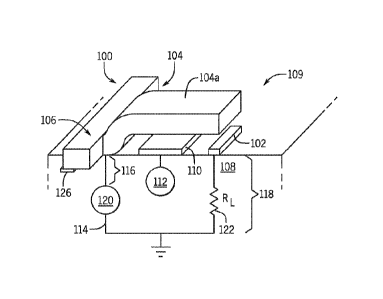
Referring to FIGS. 1-3, several views are shown of a switch structure 100
configured in accordance with an exemplary embodiment. The exemplary switch
structure 100 includes a contact 102, which at least partially comprises a
conductive
material (e.g., a metal). The switch structure 100 also includes a conductive
element,
illustrated as a cantilevered beam 104, comprising conductive material (e.g.,
a metal).
A cantilevered portion 104a of the beam 104 extends over the contact 102. In
some
embodiments, the conductive element may also include other features, such as,
for
example, a protective (and possibly non-conductive) coating on the beam 104 or
a
contact pad disposed along the portion of the beam intended to make contact
with the
contact 102. The beam 104 is supported by an anchor structure 106, from which
the
cantilevered portion 104a extends, and which may be integrated with the beam
104.
The anchor structure 106 serves to connect the cantilevered portion 104a of
the beam
104 to an underlying support structure, such as the illustrated substrate 108.
In the
embodiment of the switch structure 100 shown in FIGS. 1-3, both the contact
102 and
the anchor structure 106 are formed on the substrate 108 with conventional
microfabrication techniques (e.g., electroplating, vapor deposition,
photolithography,
wet and/or dry etching, etc.).
[0029] The switch structure 100 may constitute a portion of a
microelectromechanical or nanoelectromechanical device or a
microelectromechanical
system (MEMS) switch 109. For example, the contact 102 and beam 104 may have
dimensions on the order of ones or tens of nanometers or micrometers. In one
embodiment, the beam 104 may have a surface area-to-volume ratio that is
greater than
or equal to 108 m-1, while in another embodiment the ratio may be closer to
103 m-1.
6
Date Recue/Date Received 2022-05-05
277298-4
[0030] Integrated circuitry may be formed on the substrate 108, e.g.,
including
metal-oxide-semiconductor field effect transistors (MOSFETs) and patterned
conductive layers (not shown) that serve to provide electrical connections
among the
various components. Such patterned conductive layers may also provide
electrical
connections to the contact 102 and beam 104 (the connection to the latter
being, for
example, through the anchor structure 106), which connections are shown
schematically
in FIGS. 1 and 2 and described below. The semiconductor devices and conductive
layers, like the features of the switch structure 100, can also be fabricated
using
conventional micro-fabrication techniques. In one embodiment, the substrate
108 may
be a portion of a monocrystalline semiconductor wafer that has been processed
so as to
include one or more MOSFETs, with the switch structure 100 and other circuitry
formed on a surface of the wafer. The switch structure 100 may be disposed
over one
of the MOSFETs (e.g., along a line normal to the surface of the wafer) and may
be
operable along with the MOSFET, with the switch structure 100 and substrate
108 being
formed via a wafer level bonding. The switch structure 100 may be encapsulated
by one
or more encapsulating layers (not shown), which make up a wafer level package
(WLP)
around the switch structure 100, with the encapsulating layers forming a
substantially
hermetically sealed cavity about the switch structure 100 that is generally
filled with an
inert gas.
[0031] Referring also to FIGS. 4 and 5, the beam 104 can be configured
to be
selectively moveable between a first, non-contacting or "open" position, shown
in FIG.
4, in which the beam is separated from the contact 102 by a separation
distance d, and a
second, contacting or "closed" position, shown in FIG. 5, in which the beam
comes into
electrical contact with the contact 102. For example, the beam 104 can be
configured to
undergo deformation when moving between the contacting and non-contacting
positions, such that the beam is naturally disposed (i.e., in the absence of
externally
applied forces) in the non-contacting position and may be deformed so as to
occupy the
contacting position while storing mechanical energy therein. In other
embodiments, the
undeformed configuration of the beam 104 may be the contacting position.
7
Date Recue/Date Received 2022-05-05
277298-4
[0032] The switch structure 100 may also include an electrode 110 which,
when
appropriately charged, provides a potential difference between the electrode
and the
beam 104, resulting in an electrostatic force that pulls the beam toward the
electrode
and against the contact 102. With application of sufficient voltage to the
electrode 110,
the electrostatic force deforms the beam 104 and thereby displaces the beam
from the
non-contacting (i.e., open or non-conducting) position shown in FIG. 4 to the
contacting
(i.e., closed or conducting) position shown in FIG. 5. Therefore, the
electrode 110 may
act as a "gate" with respect to the switch structure 100, with voltages
(referred to as
"gate voltages") applied to the electrode 110 serving to control the opening
or closing
of the switch structure. The electrode 110 may be in communication with a gate
voltage
source 112, so that a gate voltage VG may be selectively applied to the
electrode 110.
[0033] The contact 102 and the beam 104 are components of the circuit
114. The
exemplary circuit 114 has a first side 116 and a second side 118 that, when
disconnected
from one another, are at different electric potentials relative to one another
(as where
only one of the sides is connected to a power source 120). The contact 102 and
beam
104 can be respectively connected to either of the sides 116, 118 of the
circuit 114, such
that deformation of the beam between the first and second positions acts to
respectively
pass and interrupt a current therethrough. The beam 104 may be repeatedly
moved into
and out of contact with the contact 102 at a frequency (either uniform or non-
uniform)
that is determined by the application for which the switch structure 100 is
utilized.
When the contact 102 and the beam 104 are separated from one another, the
voltage
difference between the contact and beam is referred to as the "stand-off
voltage."
[0034] In one embodiment, the beam 104 may be in communication (e.g.,
via the
anchor structure 106) with the power source 120, and the contact 102 may be in
communication with an electrical load 122 having a load resistance RE The
power
source 120 may be operated as a voltage source or a current source. The beam
104 acts
as an electrical contact, allowing a load current (e.g., with an amplitude
greater than or
equal to about 1 mA and an oscillation frequency of about 1 kHz or less) to
flow from
the power source 120 through the beam 104, into the contact 102 and to the
electrical
load 122 when the beam is in the contacting position, and otherwise disrupting
the
8
Date Recue/Date Received 2022-05-05
277298-4
electrical path and preventing the flow of current from the power source to
the load
when the beam is in the non-contacting position. The above-indicated current
and
switching frequency might be utilized in relatively higher power distribution
applications. In other embodiments, such as in applications where the switch
structure
100 will be utilized in a signaling context (often operating at relatively
lower powers),
the power source 120 may provide a current having a magnitude of 100 mA or
less (and
down to the 1 µA range) with a frequency of oscillation greater than 1 kHz.
[0035] The above-described switch structure 100 could be utilized as
part of a circuit
including other switch structures, whether similar or dissimilar in design, in
order to
increase the current and voltage capacity of the overall circuit. Such switch
structures
could be configured in series or in parallel to facilitate an even
distribution of stand-off
voltage when the switch structures are open and an even distribution of
current when
the switch structures are closed.
[0036] It is recognized that the MEMS switch 109 experiences thermal
cycles with
extreme temperature ranges during manufacturing and operation thereof For
example,
during manufacture, assembly, and/or operation of the MEMS switch 109, the
temperature of the MEMS switch 109 can range from 25 C to in excess of 300 C
(e.g.,
400 C) ¨ such as during an annealing step performed as part of a wafer level
bonding
process. Exposure of the MEMS switch 109 to this range of temperatures can
lead to a
problem of undesirable deformation of the switch structure 100 ¨ i.e., of the
cantilevered beam 104 ¨ that results from changes in the strain state of the
switch
structure. The change in strain rate can result from a significant difference
in the CTE
between materials in the MEMS switch 109 as well as annealing of the substrate
108
(due to several effects such as void reduction, grain growth, etch), with the
change in
strain rate causing recoverable and non-recoverable deformations of the
cantilevered beam 104 that can potentially cause the switch structure 100 to
become
non-functional if severe enough in magnitude.
[0037] To reduce the impact of any strain mismatch between the substrate
108 and
the switch structure 100, embodiments of the invention provide a switch
structure 100
9
Date Recue/Date Received 2022-05-05
277298-4
having an anchor structure 106 with a 3-D deformed structure that compensates
for
typical takeoff angle deformation of the cantilevered beam 104 resulting from
the strain
mismatch ¨ i.e., a self-compensating anchor structure. Referring again to FIG.
1 and
now additionally to FIG. 6, the anchor structure 106 of switch structure 100
is shown in
greater detail according to an exemplary embodiment. As shown in FIGS. 1 and
6, the
anchor structure 106 is formed/attached to cantilevered beam 104 such that the
anchor
structure 106 is oriented orthogonal to the cantilevered portion 104a of the
beam 104.
The anchor structure 106 includes thereon one or more anchor connections 126
by
which the anchor structure 106 and cantilevered beam 104 are mechanically
connected
to the substrate 108. According to an exemplary embodiment, the one or more
anchor
connections 126 are provided as a single/unitary element that can generally be
described
as a shaped anchor connection. The single shaped anchor connection 126 is
structured
such that a cross-section of the shaped anchor connection 126 taken orthogonal
to the
cantilevered beam 104 would pass through more than one region of the shaped
anchor
connection¨ i.e., there would be at least two distinct regions (generally
identified as 128
and 130) where the shaped anchor connection mechanically connects the anchor
106/beam 104 to the substrate 108. Furthermore, the single shaped anchor
connection
126 is formed and positioned on anchor structure 106 such that the connection
is
symmetrical about a longitudinal axis 132 of the cantilevered beam 104.
[0038]
Referring to the particular embodiment of FIG. 6, the anchor connection is
constructed as a C-shaped anchor connection 126 that is symmetrical about the
longitudinal axis 132 of the cantilevered beam 104. However, according to an
alternative embodiment, an anchor connection 134 on the anchor structure 106
may be
constructed as a V-shaped anchor connection that is symmetrical about the
longitudinal
axis 132 of the cantilevered beam 104, as illustrated in FIG. 7. In either of
these
embodiments, the anchor connection 126, 134 provides for the anchor structure
106 to
act as a self-compensating anchor structure that compensates for typical
takeoff angle
deformation of the cantilevered beam 104 resulting from the strain mismatch.
That is,
during periods of strain mismatch between the substrate 108 and the switch
structure
100 - such as at temperatures exceeding 300 C - the cantilevered portion 104a
of the
Date Recue/Date Received 2022-05-05
277298-4
beam 104 undergoes deformation so as to have a "takeoff angle" relative to the
substrate
108, i.e. deflects toward the substrate 108 in a z-direction. The construction
of the
anchor connection 126, 134, along with the general orientation thereof in a
direction
orthogonal to the orientation of the cantilevered portion 104a, functions to
compensate
for this takeoff angle by utilizing a strain gradient in an orthogonal
direction to the
takeoff angle. This strain operates through Poisson's ratio - i.e., the
negative ratio of
transverse to axial strain - of the cantilevered beam metal to effectively
pull the
cantilevered portion 104a of beam 104 back into an undeflected/undeformed
position.
That is, when the cantilevered portion 104a is strained relative to the
substrate 108 (i.e.,
strain mismatch), a portion of the strain is directed orthogonal to the
cantilevered
portion 104a, with this portion of the strain warping the anchor structure 106
enough to
compensate for the strain gradient from the substrate 108 to the top of the
anchor
structure 106. In other words, the portion of strain mismatch directed
orthogonal to the
cantilevered portion 104a develops a gradient of strain normal to the
substrate 108, so
as to pull the cantilevered portion 104a back into an undeflected or
undeformed
position. According to an exemplary embodiment, the strain directed
orthogonally to
the cantilevered portion 104a extends less than 20% of the length of the
cantilever beam
104 ¨ with this length to which the strain extends being sufficient to prevent
deflection
of the cantilevered portion 104a. Accordingly, the construction of the anchor
structure
106 as a self-compensating anchor structure results in a cantilevered beam 104
that is
totally self-compensating, which means that the same strain that causes the
takeoff
angle of the cantilevered portion 104a is also used to compensate and pull the
beam 104
flat.
[0039]
Referring now to FIGS. 8 and 9, strain maps 136, 138 are provided that
illustrate the level/magnitude of strain experienced by the overall
cantilevered beam 104
and by the anchor structure 106, respectively, for an anchor connection 126
provided as
in FIG. 6 (i.e., a C-shaped anchor connection). The strain maps 136, 138
illustrate that a
maximum amount of strain is experienced adjacent the anchor structure 106 and
that a
minimum amount of strain is experienced at the distal end of the cantilevered
portion
104a. The strain orthogonal to the cantilevered portion 104a, experienced
adjacent
11
Date Recue/Date Received 2022-05-05
277298-4
anchor connection 126, warps the anchor structure 106 enough to compensate for
the
strain gradient from the substrate 108 to the top of the anchor structure 106,
therefore
pulling the cantilevered portion 104a back into an undeflected/undeformed
position.
[0040] Referring now to FIGS. 10 and 11, switch structures 100 are shown
that each
include a self-compensating anchor structure 106 according to additional
embodiments
of the invention. The switch structures 100 of FIGS. 10 and 11 are formed to
each
include two distinct cantilevered beams 104, 140 that are attached to the same
anchor
structure 106. The cantilevered beams 104, 140 are arranged such that a first
beam 104
extends out from the anchor structure 106 in a first direction and a second
beam 140
extends out from the anchor structure 106 in a second direction that is
opposite the first
direction. While not shown in FIGS. 10 and 11, it is recognized that in
operation, each
of the beams 104, 140 is selectively moved relative to a respective contact,
such that a
cantilevered portion 104a, 140a of each beam moves between a first, non-
contacting or
"open" position and a second, contacting or "closed" position, with an
electrode 110
providing a potential difference between the electrode and the beam 104, 140
to
generate an electrostatic force that pulls the beam toward the electrode and
against the
contact 102, similar to what is shown and described in FIG. 1.
[0041] According to embodiments of the invention, in a switch structure
100 that
includes two distinct cantilevered beams 104, 140 positioned in a back-to-back
arrangement, the anchor structure 106 may function as a self-compensating
anchor
structure by properly shaping an anchor connection of the anchor structure
106. That is,
a shaped anchor connection is provided on anchor structure 106 that is
symmetrical
about a longitudinal axis 132 of the cantilevered beams 104, 140 and about an
axis
orthogonal to the cantilevered beams that passed through a midpoint of the
anchor
structure ¨ indicated at 142. According to exemplary embodiments of the
invention, the
shaped anchor connection could be constructed as an I-shaped anchor connection
144 as
illustrated in FIG. 10, or as an X-shaped anchor connection 146 as illustrated
in FIG. 11.
In each of the embodiments, the anchor connection 144, 146 provides for the
anchor
structure 106 to act as a self-compensating anchor structure that compensates
for typical
takeoff angle deformation of either/both of the cantilevered beams 104, 140
resulting
12
Date Recue/Date Received 2022-05-05
277298-4
from a strain mismatch between the substrate 108 and the switch structure 100 -
such as
might occur at temperatures exceeding 300 C. The construction of the anchor
connections 144, 146 functions to compensate for this takeoff angle
deformation of the
cantilevered portion 104a, 140a of each beam by directing a portion of strain
orthogonal
to the cantilevered portions 104a, 140a, with this portion of the strain
developing a
gradient of strain normal to the substrate 108 that warps the anchor structure
106 so as
to pull the cantilevered portions 104a, 140a back into an undeflected or
undeformed
position.
[0042]
Referring now to FIG. 12, according to another embodiment of the invention,
it is recognized that rather than having a single/unitary anchor connection on
the anchor
structure 106, two or more distinct anchor connections 148, 150 may be
provided on the
anchor connection that mechanically connect the anchor structure 106 and beam
104 to
the substrate 108. The two
or more distinct anchor connections 148, 150 are
sized/shaped, positioned, and angled on the self-compensating anchor structure
106
based on design considerations of the switch structure 100 in order to
counteract/compensate for strain experienced by the cantilevered beam 104.
That is, the
two or more distinct anchor connections 148, 150 are sized/shaped, positioned,
and
angled on the self-compensating anchor structure 106 in order to direct a
suitable
portion of a strain mismatch between the substrate 108 and the switch
structure 100
orthogonally to the cantilevered portion 104a to warp the anchor structure 106
and
compensate for the takeoff angle of the cantilevered portion in a desired
fashion. As
one example, the anchor structure 106 may be constructed such that a pair of
anchor
connections 148, 150 is provided that have dimensions of 8x8 micrometers and
are
spaced 10 micrometers apart. As another example, the anchor structure 106 may
be
constructed such that a pair of anchor connections 148, 150 is provided that
have
dimensions of 8x8 micrometers and are spaced 30 micrometers apart.
[0043] In each
of the embodiments of FIGS. 6, 7, and 10-12, it is recognized that the
thickness of the cantilevered beam 104, 140 and the materials from which it is
formed
may also be selected ¨ in conjunction with the sizing, geometry, and spacing
of the
anchor connection(s) ¨ to counteract/compensate for strain experienced by the
13
Date Recue/Date Received 2022-05-05
277298-4
cantilevered beam 104, 140. According to embodiments, the cantilevered beam
104,
140 of the switch structure 100 can be a layer comprising nickel (Ni)-12
atomic percent
tungsten (W), or nickel (Ni)-20 atomic percent tungsten (W). The cantilevered
beam
104, 140 may also be formed of what are defined as "creep resistant" materials
¨ with
the term creep resistance as used herein referring to the ability of a
material to resist
time-dependent plastic deformation when subjected to continual loads or
stresses. In
such embodiments, the cantilevered beam 104, 140 may be formed of superalloys,
including Ni-based and/or cobalt (Co)-based superalloys, Ni--W alloys, Ni--Mn
alloys,
gold containing small amounts of Ni and/or Co ("hard gold"), W,
intermetallics,
materials subject to solid solution and/or second phase strengthening, and
materials
having a crystal structure which inhibits plastic deformation, such as
hexagonal
structures or materials with low stacking fault energies. Other binary alloys,
including
any combination of Al, Ti, Cr, Mn, Fe, Co, Ni, Cu, Zn, Nb, Mo, Ag, Ta and W,
may
also be used to form the cantilevered beam 104, 140.
[0044]
Beneficially, embodiments of the invention thus provide a MEMS switch and
associated switch structure with a cantilevered beam and self-compensating
anchor
construction that reduce the impact of any strain mismatch between the switch
structure
and the substrate on which it is formed, such that the cantilevered beam is
maintained in
an undeflected or undeformed position. By providing a shaped anchor
connection(s) to
connect the anchor to the substrate, the typical takeoff angle deformation of
a cantilever
beam is compensated for via utilizing of a strain gradient in an orthogonal
direction to
the takeoff angle. That is, when there is strain relative to the substrate, a
portion of the
strain is directed orthogonal to the cantilever beam, so as to warp the anchor
enough to
compensate for the strain gradient from the substrate to the top of the anchor
¨ with the
strain operating through the Poisson ratio beam metal to effectively pull the
cantilever
beam back into position. As a result, the structure is insensitive to total
strain level,
thereby giving flexibility in the final strain state of the material and, in
turn, providing
flexibility in the processing of the switch structure.
[0045] According to one embodiment of the invention, a MEMS switch includes a
substrate and a switch structure formed on the substrate, with the switch
structure
14
Date Recue/Date Received 2022-05-05
277298-4
further including a conductive contact formed on the substrate, a self-
compensating
anchor structure coupled to the substrate, and a beam comprising a first end
and a
second end, the beam integrated with the self-compensating anchor structure at
the first
end and extending out orthogonally from the self-compensating anchor structure
and
suspended over the substrate such that the second end comprises a cantilevered
portion
positioned above the conductive contact. The cantilevered portion of the beam
undergoes deformation during periods of strain mismatch between the substrate
and the
switch structure so as to have a takeoff angle relative to the substrate, and
the self-
compensating anchor structure directs a portion of the strain mismatch
orthogonally to
the cantilevered portion so as to warp the anchor and compensate for the
takeoff angle
of the cantilevered portion.
[0046]
According to another embodiment of the invention, a method of
manufacturing a MEMS switch includes providing a substrate and forming a
switch
structure on the substrate via a wafer level bonding process. Forming the
switch
structure further includes forming a conductive contact on the substrate,
forming a self-
compensating anchor structure, and attaching a cantilevered beam to the self-
compensating anchor structure to position the cantilevered beam relative to
the substrate
and the conductive contact, the cantilevered beam comprising a cantilevered
portion at
an end thereof opposite the self-compensating anchor structure, with the self-
compensating anchor structure being arranged orthogonally to the cantilevered
portion
of the cantilevered beam and with the cantilevered portion extending out so as
to be
spaced apart from the substrate and positioned above the conductive contact.
The
method also includes performing an annealing process on the substrate and the
switch
structure to achieve bonding in the MEMS switch. The cantilevered portion of
the
beam undergoes deformation during the annealing process responsive to a strain
mismatch between the substrate and the switch structure, such that the
cantilevered
portion has a takeoff angle relative to the substrate, and the self-
compensating anchor
structure directs a portion of a strain resulting from the strain mismatch
orthogonal to
the cantilevered portion so as to warp the anchor structure and compensate for
the
takeoff angle of the cantilevered portion.
Date Recue/Date Received 2022-05-05
277298-4
[0047] According to yet another embodiment of the invention, a MEMS switch
includes a substrate and a switch structure formed on the substrate, with the
switch
structure further including a conductive contact formed on the substrate, an
anchor
structure coupled to the substrate, and a beam integrated with the anchor
structure and
extending out orthogonally therefrom, the beam comprising a cantilevered
portion
suspended over the substrate and positioned above the conductive contact. The
anchor
structure comprises a self-compensating anchor structure that causes the
cantilevered
portion to remain undeflected when subjected to thermally induced takeoff
angle
deformation.
[0048] This written description uses examples to disclose the invention,
including
the best mode, and also to enable any person skilled in the art to practice
the invention,
including making and using any devices or systems and performing any
incorporated
methods. The patentable scope of the invention is defined by the claims, and
may
include other examples that occur to those skilled in the art. Such other
examples are
intended to be within the scope of the claims if they have structural elements
that do
not differ from the literal language of the claims, or if they include
equivalent structural
elements with insubstantial differences from the literal languages of the
claims.
[0049] While the invention has been described in detail in connection
with only a
limited number of embodiments, it should be readily understood that the
invention is not
limited to such disclosed embodiments. Rather, the invention can be modified
to
incorporate any number of variations, alterations, substitutions or equivalent
arrangements not heretofore described, but which are commensurate with the
spirit and
scope of the invention. Additionally, while various embodiments of the
invention have
been described, it is to be understood that aspects of the invention may
include only
some of the described embodiments. Accordingly, the invention is not to be
seen as
limited by the foregoing description, but is only limited by the scope of the
appended
claims.
16
Date Recue/Date Received 2022-05-05