Note: Descriptions are shown in the official language in which they were submitted.
1
METHOD FOR WELDING METAL-BASED MATERIALS
The present invention relates to a method for welding metal-based materials by
using a welded spacer, which makes possible to use resistance welding in
connection with joining of materials otherwise non-weldable to each other by
resistance welding.
The resistance welding is one of the most used welding procedures in metal
manufacturing industries. The resistance welding can be carried out for
instance by spot welding, roller seam welding or weldbonding welding in order
to have welded white goods, fuel tanks, body construction of cars, railways or
trucks. But there are a lot of materials, such as hot formed martensitic
stainless
steel or two and three material combinations which do not have weldability for
a
resistance welding process. For those materials there are several ideas to
create mechanical solder or brazing depots on the material. However, those
mechanical solder or brazing depots require deformation and/or cutting of the
material in order to have good bond between the material and the mechanical
solder or brazing depots. When the materials are further treated by the
traditional resistance welding processes the weld spot has typically as
results
cold cracks brittle fracture behaviour and therefore and therefore low
strength
level.
The mechanical solder or brazing depots before the welding process are
difficult to use especially in the course of multi-material-design. Further,
mechanical solder or brazing depots will cause an increase in manufacturing
costs.
The EP patent application 1582283 relates to a process for spot welding of two
rigid steel sheet parts where small platelets, preferably of easily welded
metal
such as low-carbon iron, are arranged between the sheets at the welding
points. Before spot welding the material to be welded is normally transferred
from one position to another. Using platelets not fixed with the material to
be
Date Recue/Date Received 2022-09-27
CA 02978373 2017-08-31
WO 2016/146511 PCT/EP2016/055259
2
welded there is a great danger that the platelets will move from their desired
position during transferring. The EP patent application 1582283 has not
indicated anything about this kind of a danger.
The DE patent application 2541963 describes a process for joining two or more
shaped metal parts, using a sealant between all the joint surfaces, the
sealant
contains individual round grins of metal, or another material, with a
controlled
grain-size, and the two metal parts being joined are brought together leaving
a
gap determined by the preselected grain-size; the parts are then joined by, or
via the sealant. Thus in the DE patent application 2541963 two metal parts are
welded together with traditional spot welding, not considering the fact that
the
metal parts are not able to be welded by spot welding.
The JP patent application S59229293 relates to a method for joining securely
different metallic plates while forming a clearance between both metallic
plates
by interposing an insert piece by solid-phase joining of respective metals
between the different metallic plates which permit fusion joining. The method
of
the JP patent application S59229293 uses rotating tools for friction welding.
This kind of process is suitable for materials, such as titanium and aluminium
which are able for plastification, not suitable for stainless steels or more
generally for steels.
For welding of especially stainless steels it is generally used the Schaeffler
diagram which defines the microstructure areas in the steels by means of the
chromium equivalent (Creq) and the nickel equivalent (Nieq). In the diagram
the
Creq and Nieq are calculated according to the following formulas
Creq = %Cr + % Mo + 1,5x /0Si + 0,5x /0Nb + 0,5x%Ti (1)
Nieq = %Ni + 30x( /0C + %N) + 0,5x /0Mn (2).
CA 02978373 2017-08-31
WO 2016/146511 PCT/EP2016/055259
3
The Schaeffler diagram provides information on the welding properties of the
various types of microstructure, thus as a function of what alloying elements
they contain.The Schaeffler diagram is also classified with welding problems,
having different areas for hot cracking, cold crack, grain growth and
embrittlement.
The US patent 4959518 describes welding of studs in accordance with the
Schaeffler diagram. Also the US patent 5622573 uses the Schaeffler diagram
in welding for a material having been overlaid onto a cast iron base metal.
The
WO publication 2011/060432 describes the use of the Schaeffler diagram for
dissimilar joints between a TWIP steel and a carbon steel with laser beam
welding. However, these publications do not describe anything about
resistance welding.
In the Fig. 7 hereafter the Schaeffler diagram is illustrated with hot
cracking
area, cold crack area, grain growth area and embrittlement.area. The Fig. 7 is
also provided with an example of welding problems. In this example a
resistance spot welding between a martensitic stainless steel 1.4304 (steel 1)
and an unalloyed carbon steel (steel 2) is not possible because the resultant
alloy (R) created in the resistance welding is still in the cold cracking area
and
thus the weld nugget between those steels is with cold cracks and thus not
valuable for the use.
The object of the present invention is to eliminate some drawbacks of the
prior
art and to achieve a welding method containing resistance welding as at least
one process step with metal-based materials, which are non-weldable with the
resistance welding. A connection between metal-based materials, non-weldable
directly to each other by the resistance welding, is established with a
spacer,
which is joined by welding to the material before the resistance welding. The
essential features of the present patent application are enlisted in the
appended claims.
CA 02978373 2017-08-31
WO 2016/146511 PCT/EP2016/055259
4
According to the present invention, a method for welding of at least two metal-
based materials, non-weldable directly to each other with resistance welding,
contains at least one joining process step by welding before a resistance
welding step. In the case with only two metal-based materials, wherein both
the
materials are non-weldable to each other by resistance welding, the first step
is
to join a spacer preferably to one of those materials, described as the first
material to be welded. It is also possible to join a spacer to both materials.
In
the second step of the method according to present invention the spacer is
utilized so that the resistance welding is focused on the surface of the
spacer in
the first material to be welded and to the surface of the other material to be
welded. Thus a welding joint is achieved between two materials directly non-
weldable to each other with resistance welding. In the case with two metal-
based materials, wherein one of the materials is non-weldable by resistance
welding, the spacer is welded on the surface of the non-weldable material by
resistance welding. In the case, there are more than two metal-based
materials,
non-weldable directly to each other by resistance welding, in utilizing the
method of the present invention at least one spacer is joined by welding on
the
surfaces of the materials in every interstice between two surfaces of
materials
to be welded on at least one of the two surfaces, directly non-weldable to
each
other with resistance welding.
The spacer according to the present invention is advantageously created of a
filler material or a braze material. The material of the spacer is dependent
on
the material on which surface the spacer is joined in order to have a good
contact and high strength between the spacer and the joined metal-based
material. When using a brazing material as the spacer, the microstructure of
the
material to be welded will not be destroyed during the method of the present
invention. Additionally, a good plug fracture in the spacer is required for
successful processing with the resistance welding.
The shape of the spacer in accordance with the present invention can be
essentially sheet-like. However, it is advantageous to use the essentially
sheet-
CA 02978373 2017-08-31
WO 2016/146511 PCT/EP2016/055259
like material as a substrate so that the essentially sheet-like material is
provided
with protrusions. The protrusions are positioned essentially regularly so that
the
protrusions are spaced a defined distance apart from each other. The
construction of the spacer gives a proportion of diameter to height for the
5 spacer at least five. Further, the height of a spacer is advantageously at
least
0.5 millimeter in order to achieve a desired gap between the materials welded
in accordance with the present invention.
After the joining the spacer on the desired surface of a material, the
resistance
welding is advantageously focused on the surface of the spacer in the first
material and on the surface of the other material in order to achieve a weld
between the first material and the other material for producing a desired
construction, containing materials, otherwise non-weldable directly to each
other with resistance welding. However, for the resistance welding it is also
possible to utilize a bypass effect, in which case the heating during
resistance
welding causes a physical effect on the heat affecting zone on the surface to
be
welded. This effect causes spacers located on the heat affecting zone to be
melted. Therefore, it is possible to focus the resistance welding on the area
between spacers located on the heat affecting zone. The bypass effect causes
adjacent spacers to be melted, and thus a successful resistance welding is
carried out. The same effects are also considered when spacers are joined to
both materials so that the surfaces of the spacers which are opposite to the
surfaces of the spacers joined to the materials to be welded have contact with
each other before resistance welding.
It is also possible to utilize the method of the invention so that a spacer is
joined
to one material and then the material with the spacer is resistance welded
with
two or more materials, weldable directly to each other with resistance
welding.
In this case the two or more materials, weldable directly to each other with
resistance welding, are positioned in the opposite side to the surfaces of the
materials non-weldable directly to each other with resistance welding, between
which surfaces the spacer is positioned. The resistance welding is thus
CA 02978373 2017-08-31
WO 2016/146511 PCT/EP2016/055259
6
focussed to the first material having the spacer, to the spacer itself and to
at
least one intermediate material which is directly resistance welded with one
other material. Using a spacer in this kind of combination it makes possible
to
control and to have a desired direction for the welding heat. In one
embodiment
applying the control of welding heat a spacer with a low thermal conductivity
is
welded to a thin sheet or to a material with a high thermal conductivity. Then
the intermediate material is a thicker sheet or has a lower thermal
conductivity
than the first material with the spacer. One another advantage based on the
use of a spacer is that the spacer can avoid liquid metal embrittlement of
resistance spot welds between austenitic steels and a zinc coating of the
other
sheet. The spacer can be made with a ferritic filler metal and shows no liquid
metal embrittlement, and because of the distance/gap between the two sheets,
liquid metal embrittlement is avoid in the austenitic sheet. In this case the
spacer must be welded at first to the zinc coated sheet.
The joining of the spacer, as the first process step in the method of the
present
invention, is carried out advantageously by welding using arc welding or beam
welding. The process step using arc welding can be carried out by for instance
plasma welding, gas metal arc welding, such as TIG (Tungsten Inert Gas)
welding or MIG (Metal Inert Gas) welding. The process step using beam
welding can be carried out by laser beam welding or electron beam welding.
Naturally, other welding methods except resistance welding can be used in the
joining of the spacer according to the present invention.
The resistance welding process step in accordance with the present invention
can be carried out by different kinds of the resistance welding, such as spot
welding, roller seam welding, projection welding or weldbonding. Weldbonding
is a combination of the conventional resistance spot welding and adhesive
bonding. When in the resistance welding bonding is the result of heat and
pressure, the adhesive join consists of an adhesive film strip applied between
the both surfaces to be joined. With regard to the projection welding, which
is a
CA 02978373 2017-08-31
WO 2016/146511 PCT/EP2016/055259
7
modification of the resistance welding, the weld is localized by means of
raised
projections on one or on both of the workpieces to be welded.
According to the present invention there is no contact corrosion between the
dissimilar joining materials. The spacer reduces the contact corrosion between
two materials to be welded. According to the prior art the materials are
directly
in contact with each other. With the construction of the spacer there is a
defined gap between the two materials and the joint place. The spacer can be
specifically alloyed to avoid the corrosion problem and makers possible to use
also materials having different electrochemical potentials.
Using the method of the present invention with the described construction of
the spacer achieves a desired gap between the welded materials and a better
wetting of cathodic dip coating in crevice conditions and, thus no crevice
corrosion or cranny corrosion exists Instead of cathodic dip coating, other
coating methods or painting methods can be used, such as ground coating,
priming coating, undercoating, structure coating and welding primer coating.
One another possible solution of the present invention is for tubes where:an
inner tube is welded with spacer at the outer side and then a second tube is
imposed, having contact to the spacer and, further, the combination is
resistance welded to each other.. As a result the tubes have a defined gap to
each other because of the spacer. The spacer can also be used to separate the
tubes in point of electrochemical corrosion potential. The gap achieved by the
spacer can also be utilized for cooling or heating with air or a fluid medium.
The method of the present invention can be utilized for instance in the
automotive industry and for busses, trucks and railway vehicles, because of
the
good behaviour in combination with a hybrid joining process, such as
weldbonding. In weldbonding, when using a spacer according to the present
invention it is prevented to create a steam channel in an adhesive, because
the
spacer replaces the adhesive material at the area of the following resistance
CA 02978373 2017-08-31
WO 2016/146511 PCT/EP2016/055259
8
welding area. Therefore, there is essentially no way for corrosive substance
to
reach the welding area.
The invention is described in more details in the following referring to the
drawings, wherein
Fig. 1 illustrates one preferred embodiment of the invention schematically
from
the side view,
Fig. 2 illustrates another preferred embodiment of the invention schematically
from the side view,
Figs. 3a, 3b and 3c illustrates a preferred embodiment of the invention
schematically from the side view,
Figs. 4a and 4b illustrates a preferred embodiment of the invention
schematically from the side view,
Fig. 5 illustrates still one preferred embodiment of the invention
schematically in
cross-section,
Fig. 6 shows an example to use the Schaeffler diagram in accordance with the
invention, and
Fig. 7 illustrates, as described in the prior art of the invention, Schaeffler
diagram with an example of problems in the prior art.
The materials, non-weldable directly together with the resistance welding, to
be
used in the method of the present invention can be for instance steels which
are out of the Schaeffler diagram. In general, the steels containing more than
0,25 weight % C, more than 3 weight % Mn, more than 0,1 weight % N and
more than 3 weight % Mo are out of the Schaeffler diagram. Furthermore it is
possible with the invention to avoid areas of the Schaeffler diagram which are
classified with welding problems as illustrated in Fig. 7. The manner to avoid
these problems is to use the spacer in a kind of an alloying element. By using
the spacer on that manner it is possible to calculate and to choose the
material
for the spacer with the Schaeffler diagram.
CA 02978373 2017-08-31
WO 2016/146511 PCT/EP2016/055259
9
Further, the materials also used in the method of the present invention are
the
steels having the carbon equivalent (CEV) more than 0,65 /0, where CEV is
calculated using a formula (element contents by weight %):
CEV = C + Mn/6 + (Cu + Ni)/15 + (Cr + Mo + V)/5.
Also other metal materials, such as aluminium, can be treated in accordance
with the present invention.
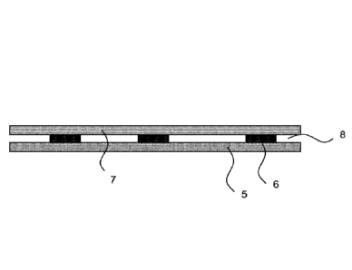
In Fig. 1 the first welded material 5 provided with a spacer 6 has been welded
by resistance welding to the second material 7. The spacer 6 has achieved a
gap 8 between the welded materials 5 and 7. The gap 8 prevents a direct
contact between the welded materials 5 and 7. Based on the gap 8 defined by
the spacer 6 the welded materials 5 and 7 can have different electrochemical
potentials without any contact corrosion.
Fig. 2 illustrates cathodic dip coating in connection with the present
invention.
The first welded material 11 provided with a spacer 12 has been welded by
resistance welding to the second material 13. The welded structure 14 is
further
treated in a coating process to have a coating layer 15, thanks to the spacer
12,
on the surface of the first material 11, on the surface of the spacer 12 and
on
the surface of the second material 13, because the spacer 12 achieves a gap
16 between the welded materials 11 and 13.
The present invention is applied for weldbonding in accordance with Figs. 3a,
3b and 3c. In Fig. 3a the first material 31 to be welded is provided with a
spacer
32 and with an adhesive material 33 for weldbonding. The Fig. 3a also shows
the welding area 34 between the first material to be welded and the spacer 32.
In Fig. 3b the second material 35 to be welded is added on the adhesive
material 33, and the welding electrodes 36 and 37 are ready to start welding
between the materials 31 and 35. Fig. 3c illustrates the result of the
weldbonding, a nugget weld 38, between the spacer and the second welded
CA 02978373 2017-08-31
WO 2016/146511 PCT/EP2016/055259
material 35. Because the adhesive material 33 was not splashed out, there is
no stream channel between the materials 31 and 35.
Fig. 4a illustrates an embodiment where spacers 23 and 24 are welded to the
5 first material 21, and spacers 25 and 26 are welded to the second material
22.
As illustrated in Fig. 4b the material 21 and 22 are spot welded in order to
have
a weld nugget 28 using the spacers 23 and 24 and respectively 25 and 26.
Based on the spacers 23 and 25 and respectively 24 and 26 on the both
materials 21 and 22 the gap 27 is thus larger than in the embodiment of Fig. 1
10 that makes better to avoid contact corrosion between the materials 21 and
22.
Fig. 5 illustrates the present invention applied for a tube after resistance
welding. The inner tube 41 is first provided with a spacer 43 and then the
outer
tube 42 is imposed around the inner tube 41. The inner tube 41 and the outer
tube 42 are resistance welded to each other to achieve the weld nugget 45.
Thus a gap 44 caused by the spacer 43 is formed between the inner tube 41
and the outer tube 42.
Fig. 6 illustrates an example for the use of the Schaeffler diagram according
to
the invention. In the example the same steels as in the prior art Fig. 7, a
martensitic stainless steel 1.4034 being as the first metal 1 and an unalloyed
carbon steel being as a second metal 2 shall be welded together. For the
spacer material S it is selected a CrNi filler metal which microstructure
consists
of austenite and about 20 vol % ferrite. The spacer material S is welded with
the metal 1 by arc welding, and a resultant alloy Si is achieved between the
first metal 1 and the spacer S. When the second metal 2 is then welded by the
resistance welding with the spacer 5, the final resultant alloy S2 between the
second metal 2 and the spacer S is outside all the areas problematic for
resistance welding. Thus a desired weld result is achieved.