Note: Descriptions are shown in the official language in which they were submitted.
Apparatus for thermal treatment of a substrate, a carrier and a substrate
support element for that apparatus
Technical background
The present invention relates to an apparatus for thermal treatment of a
substrate,
said device having a heating device and a carrier provided with a support
surface
for carrying the substrate.
The present invention furthermore relates to a carrier for thermal treatment
of a
substrate, having at least one support surface for a substrate.
Finally, the present invention relates to a substrate support element for a
carrier
for thermal treatment of a substrate, having a support surface for the
substrate.
Apparatus in the context of the invention are employed, for instance, for
thermal
treatment of semiconductor wafers in the semiconductor and photovoltaic indus-
tries; they are generally designed for simultaneous irradiation of a plurality
of sub-
strates and as a rule are used in non-continuous processes (batch processes).
In
these apparatus, the substrate is normally arranged in a closed process
chamber
that is designed for thermal treatment with particular environmental
conditions; the
process chamber may preferably be evacuated or may be pressurized with a reac-
2 0 tive or protective gas.
Carriers in the context of the invention are designed to receive and hold one
or a
plurality of substrates and/or may be used for transporting the latter; these
carriers
have one or a plurality of support surfaces, each of which may be designed for
receiving one or a plurality of substrates. The carriers may be embodied in
one
piece or in multiple pieces. In the latter case, the carrier frequently has a
holding
frame in which one or a plurality of substrate support elements may be
received.
Substrate support elements in the context of the invention have at least one
sup-
port surface for carrying a substrate, for instance in the form of a
depression. They
are used, for instance, as holders or carriers for one or a plurality of
substrates.
CA 2978448 2017-09-05
- 2 -
Prior art
During the production and processing of silicon wafers, it is frequently
necessary
to subject the silicon wafers to a thermal treatment. Silicon wafers are thin,
wafer-
shaped substrates that have a substrate top side and a substrate bottom side.
For
the thermal treatment of silicon wafers, apparatus are used that have a
heating
device, generally in the form of one or a plurality of infrared emitters, in
addition to
a substrate receiving element.
Since thermal treatment of silicon wafers frequently occurs under special
condi-
tions ¨ for instance in a vacuum or in another, suitable atmosphere, for
instance a
reactive atmosphere ¨ the substrate receiving element is generally located in
a
gas-tight closed process chamber. High throughput of the wafers is achieved
dur-
ing the thermal processing when a plurality of wafers is subjected to the
thermal
treatment in the process chamber at the same time. To this end, the wafers are
advantageously held on a carrier that - loaded with the plurality of wafers -
are
supplied to thermal treatment.
Such carriers frequently have vertical structures; they essentially comprise
an up-
per and a lower limiting plate that are joined to one another by a plurality
of slotted
transverse bars. During the technical processing of wafers for semiconductors,
these carriers are used, for example, in a furnace, in a coating or etching
system,
but also for transporting and storing wafers. Such a carrier is known, for
example
from DE 20 2005 001 721 U1. Alternatively and in addition, horizontal
structures
are used in which the wafers are arranged in a plurality of levels like a
shelving
system.
However, a disadvantage of known carriers is that only a little assembly space
remains between the wafers held in the carrier, which leads to the heating
device
being arranged at the side of the carrier. Irradiation of the wafers from the
side is
generally linked to uneven radiation of the edge and center regions of the
wafers.
This may lead to longer processing times, since the irradiation must continue
until
even the center region of the wafer has reached the selected temperature.
CA 2978448 2017-09-05
- 3 -
In known apparatus, the infrared emitters are arranged in the process chamber
in
order to permit the highest possible irradiation intensity on the wafer
surface. A
good, uniform thermal treatment of substrates with large surface areas is
attained
when a plurality of infrared emitters are located in the process chamber. The
infra-
red emitters are generally arranged with the longitudinal axes of their
emitter tubes
parallel to one another. The infrared emitters are preferably located at the
top and
bottom sides of the substrate. However, this requires the presence of a
compara-
tively large available assembly space above and/or below the wafer that is to
be
irradiated.
The electrical contacting of the infrared emitter is generally outside of the
process
chamber. This has the advantage that electrical discharges at the contacting
sites
are avoided inside the process chamber. However, in this case the infrared
emit-
ters must be conducted through the process chamber wall so that a special seal
is
required for the feedthroughs.
From DE 10 2008 063 677 B4, for instance, an infrared emitter is known that
may
be installed in a vacuum chamber and that for gas-tight sealing is provided
with a
sealing element in form of an 0-ring. Such seals have the disadvantage,
however,
that the sealing element is regularly subjected to high thermal stresses that
can
damage the sealing element. It is therefore complicated to attain a continuous
thermal seal of feedthroughs for the infrared emitter.
Finally, the infrared emitters arranged ino the process chamber have a certain
spatial extension and require the availability of a certain amount of assembly
space. The assembly space of apparatus that are used for thermal treatment of
substrates is frequently limited and cannot be enlarged as desired. Moreover,
ad-
ditionally required assembly space may contribute to an increase in the
required
processing times, since the evacuation process is longer in apparatus having
larg-
er dimensions, for example. This may result in the throughput being reduced
dur-
ing the thermal treatment of the wafers.
CA 2978448 2017-09-05
- 4 -
Technical object
The underlying technical object of the invention is therefore to provide an
appa-
ratus that permits high substrate throughput.
Moreover, the underlying object of the invention is to provide a carrier and a
sub-
strate support element for a carrier that permits simple thermal treatment of
sub-
strates with a high throughput.
General description of the invention
With respect to the apparatus for thermal treatment of a substrate, the
aforesaid
object, starting from the aforementioned apparatus, is achieved according to
the
invention in that at least part of the carrier is produced from a composite
material
comprising an amorphous matrix component and an additional component in form
of a semiconductor material, wherein a conductor path that is part of the
heating
device and that is made of an electrically conducting resistance material that
gen-
erates heat when current passes through it is applied to the surface of the
carrier.
Known apparatus for thermal treatment of a substrate have a carrier and a
heating
device. In these apparatus, the carrier and the heating device are embodied as
separate assemblies, wherein the heating device is generally arranged in the
pro-
cess chamber adjacent to the carrier, for instance above and/or below the
carrier,
or the heating device is located at a side of the carrier. The heating device
corn-
prises a thermal radiation emitting heating element as well as the electrical
con-
nections and circuits required for operating the heating element.
The underlying idea of the present invention is that a high substrate
throughput
may be attained if the apparatus has the most compact possible design. Accord-
ing to the invention, this is attained in that no separate heating device is
used and
the heating device is integrated into the carrier. Moreover, a carrier having
an in-
tegrated heating device contributes to very uniform irradiation of a substrate
placed thereon.
CA 2978448 2017-09-05
- 5 -
According to the invention, therefore, two modifications of the carrier are
suggest-
ed, one relating to the material of the carrier and the other relating to the
type of
electrical contacting of the carrier.
To permit emission of infrared radiation by the carrier, at least part of the
carrier is
produced from a composite material. The composition of the composite material
is
selected such that a thermally excitable material is obtained that can assume
a
low-energy starting state and can assume a high-energy excited state. If such
a
material returns from the excited state to the starting state, energy is
released,
preferably in form of infrared radiation, and is available for radiating the
substrate.
The energy required for exciting the composite material is provided by a
conductor
path made from an electrically conducting resistance material that is applied
to a
surface of the carrier, the conductor path generates heat when current is
flowing
therethrough. The conductor path acts as a "local" heating element with which
at
least a portion of the carrier may be locally heated. However, the conductor
path
does not form the actual heating element with which the substrate is heated in
the
apparatus, but instead is primarily for heating another apparatus component,
spe-
cifically the carrier itself. The conductor path is dimensioned such that it
heats a
part of the carrier that is made of composite material. The transport of heat
from
the electrical resistance element to the carrier may be based on thermal
conduc-
tion, convection, or thermal radiation.
Moreover, a heating device integrated into the carrier contributes to
minimizing the
average distance from the heating element to the substrate surface. This
permits
a particularly effective heating up process and short processing times.
In an apparatus having such a carrier structure, the part of the carrier that
is pro-
duced from the composite material forms the actual element that emits infrared
radiation. The composite material includes the following components:
= The amorphous matrix component represents the largest portion of the com-
posite material in terms of weight and volume. It determines, to the greatest
extent, the mechanical and chemical properties of the composite material: for
example, its temperature resistance, strength, and corrosion properties.
CA 2978448 2017-09-05
- 6 -
Since the matrix component is amorphous ¨ it preferably comprises glass ¨
the geometric configuration of the carrier may be adapted more simply to the
requirements of the specific use of the inventive apparatus than a carrier
made of crystalline materials. Furthermore, a composite material that essen-
tially comprises an amorphous material component is easy to adapt to spe-
cial substrate shapes.
The matrix component may comprise undoped or doped silica glass and, be-
sides SiO2, may include other oxide, nitride, or carbide components in a
quantity up to a maximum of 10 wt.%.
= Moreover, according to the invention it is also provided that an
additional
component in the form of a semiconductor material is intercalated in the ma-
trix component. The additional component forms a discrete amorphous
phase dispersed in the amorphous matrix component or forms a crystalline
phase.
A semiconductor has a valence band and a conduction band that may be
separated from one another by a forbidden zone having a width of up to ZIE
3 eV. The width of the forbidden zone is for instance 0.72 eV for Ge, 1.12
eV for Si, 0.26 eV for InSb, 0.8 eV for GaSb, 1.6 eV for AlSb, 2.5 eV for CdS.
The conductivity of a semiconductor depends on how many electrons cross
the forbidden zone and can travel out of the valence band into the conduc-
tion band. In principle, at room temperature only a few electrons can cross
the forbidden zone and travel into the conduction band, so that as a rule at
room temperature a semiconductor has only limited conductivity. However,
the level of conductivity of a semiconductor is substantially dependent on the
latter's temperature. If the temperature of the semiconductor material rises,
the probability that there is enough energy available to move an electron
from the valence band to the conduction band increases, as well. Therefore,
semiconductor conductivity increases with temperature. At the right tempera-
tures, semiconductor materials have good electrical conductivity.
The additional component as a discrete phase is distributed uniformly or in-
tentionally non-uniformly. The additional component determines to a large
CA 2978448 2017-09-05
- 7 -
extent the optical and thermal properties of the substrate; more precisely, in
the infrared spectrum, that is the wavelength range between 780 nm and
1 mm, it causes absorption. For at least some of the radiation in this spec-
trum range, the additional component has an absorption that is higher than
that of the matrix component.
The phase regions of the additional component act in the matrix as optical
discontinuities and result, for example, in that the composite material may
visually appear black or blackish-gray at room temperature, depending on
layer thickness. In addition, the discontinuities themselves are heat absorb-
ing.
The additional component is preferably present in the composite material in
a manner and quantity such that in the composite material it causes a spec-
tral emittance c of at least 0.6 for wavelengths between 2 pm and 8 pm at a
temperature of 600 C.
A particularly high emittance may be attained when the additional component
is present as an additional component phase and has a non-spherical mor-
phology with maximum dimensions of on average less than 20 pm but pref-
erably more than 3 pm.
The non-spherical morphology of the additional component phase also con-
tributes to high mechanical strength and to a low tendency of the composite
material to form cracks. The term "maximum dimension" refers to the longest
extension of an insulated region with additional component phase detectible
in a micrograph. The aforesaid average is found from the mean value of all
of the longest extensions in a micrograph.
According to Kirchhoff's Radiation Law, spectral absorptivity ak and spectral
emittance Ea, of a real body in thermal equilibrium are equal.
= 62, (1)
CA 2978448 2017-09-05
' - 8 -
The additional component thus means that the substrate material emits infra-
red radiation. The spectral emissivity EX may be calculated as follows with
known targeted hemispherical spectral reflectance Rgh and transmittance Tgh:
EX = 1-Rgh ¨ To (2)
"Spectral emissivity" shall be construed to mean "spectral normal emissivity."
It
is found using the measuring principle known as "Black-Body Boundary Condi-
tions" (BBC) and published in "DETERMINING THE TRANSMITTANCE AND
EMITTANCE OF TRANSPARENT AND SEMITRANSPARENT MATERIALS
AT ELEVATED TEMPERATURES," J. Manara, M. Keller, D. Kraus, M. Arduini-
Schuster; 5th European Thermal-Sciences Conference, The Netherlands
(2008).
The amorphous matrix component in the composite material, that is, in
connection
with the additional component, has higher thermal radiation absorption than
would
be the case without the additional component. This results in improved thermal
conduction from the conductor path into the substrate, more rapid distribution
of
the heat, and a higher rate of radiation onto the substrate. Because of this
it is
possible to provide greater radiant power per unit of surface area and also to
pro-
duce a uniform emission and uniform temperature field, even with thin support
structure wall thicknesses and/or with a comparatively low conductor load
density.
A carrier having a thin wall thickness has a low thermal mass and permits
rapid
temperature change. A cooling element is therefore not necessary.
In a preferred embodiment of the apparatus according to the invention, the
addi-
tional component is present in a type and quantity that causes a spectral
emissivi-
ty s of at least 0.75 for wavelengths between 2 pm and 8 pm in the composition
material at a temperature of 1000 C.
Consequently, the composite material has a high absorption and emission capaci-
ty for thermal radiation between 2 pm and 8 pm, that is, in the wavelength
range
of the infrared radiation. This reduces the reflection on the composite
material sur-
faces so that, assuming negligibly small transmission, the result is
reflectance of a
maximum of 0.25 for wavelengths between 2 pm and 8 pm and at temperatures
CA 2978448 2017-09-05
- 9 -
greater than 1000 C and of 0.4 at temperatures of 600 C. Non-reproducible heat-
ing by reflected thermal radiation is thus avoided, which contributes to a
uniform or
desired non-uniform temperature distribution.
In a preferred embodiment of the apparatus according to the invention it is
provid-
ed that the apparatus has a process chamber in which the carrier is located,
said
process chamber has a process chamber wall with a current feedthrough through
which a first electrical potential and a second electrical potential is
conducted into
the process chamber for electrically contacting the conductor path.
An electrical supply for the conductor path is required for operating the
heating
device that is integrated in the carrier. Since only a small operating current
is re-
quired for operating the conductor path, compared to a conventional heating de-
vice, the conductor path may be electrically contacted via a single current
feed-
through into the processing space. Current feedthroughs of any type have the
dis-
advantage that they must be sealed. However, such seals are frequently problem-
atic, especially because a permanent seal is nearly impossible to achieve. The
limiting factor is frequently the standing time of the light elements used,
specifical-
ly when they are exposed to high radiant power or reactive atmospheres. One ad-
vantage of the apparatus according to invention is that even a plurality of
conduc-
tor paths of a carrier may be supplied by means of one current feedth rough,
so
that only two electrical potentials have to be conducted into the process
chamber.
Preferably only a first individual line having the first electrical potential
and a
second individual line having the second electrical potential are conducted
into the
process chamber. The first individual line and the second individual line may
be
integrated into a shared cable. The conductors connected thereto may be
switched in parallel or in series.
With respect to the carrier for thermal treatment of a substrate, the
aforesaid ob-
ject, starting from a carrier cited in the foregoing, is achieved according to
the in-
vention in that at least part of the carrier is produced from a composite
material
comprising an amorphous matrix component and an additional component in the
form of a semiconductor material, and a conductor path made of an electrically
conducting resistance material that generates heat when current flows through
it is
CA 2978448 2017-09-05
- 1 0 -
applied to a surface of the composite material.
The inventive carrier is in particular designed for thermal treatment of a
semicon-
ductor wafer (silicon wafer).
Known carriers for thermal treatment of a substrate are normally produced from
a
temperature-resistant material. Moreover, especially in semiconductor
production
the yield and the electrical operating performance of semiconductor components
depends to a very large extent on the success to prevent the semiconductor
from
being contaminated with impurities during production. To prevent contamination
from being introduced into the process chamber through the carrier, known
carri-
ers are frequently produced from a single material having a high chemical re-
sistance so that this represents a low contamination risk for the substrate.
The carrier according to the invention may be embodied in one piece or in
multiple
pieces; it may in particular have a vertical structure or a horizontal
structure. The
carrier preferably has a horizontal structure. In horizontal structures, the
support
surface for the substrate runs parallel to the surface of the floor of a
process
chamber. If a plurality of carrier elements is provided, they are arranged
parallel to
one another. Such a horizontal orientation of the substrates has the advantage
that the substrates due to gravity are positioned on its respective support
surface.
This permits good heat transfer from the support surface to the associated sub-
strate. In this context, the use of a shelving-type carrier structure has
proved par-
ticularly advantageous, since with this type of carrier the energy required
for heat-
ing the substrate may be provided via two mechanisms, specifically by direct
irra-
diation of the substrate and also indirectly by thermal conduction with the
carrier
itself.
Since the carrier according to the invention is produced from a composite
material
and at the same time is provided with a conductor path made of a resistance ma-
terial, infrared radiation may be produced directly with the carrier. The
inventive
carrier therefore has two functions: first, the carrier may be used for
transporting
and storing substrates, and second, the carrier may also be employed as a
radia-
tion source for thermal treatment of the substrates, without an additional,
external
CA 2978448 2017-09-05
-11 -
radiation source being required for this. It is also not necessary, for
instance, to
relocate substrates into a special carrier suitable for irradiating the
substrates.
According to the invention, the material from which the carrier is produced
and the
type of electrical contacting are selected such that at least some of the
carrier ma-
terial may be converted, by means of energy introduced into the material, from
a
starting state to an excited state, specifically such that during its return
from the
excited state to the starting state the carrier material emits infrared
radiation that is
provided for irradiating the substrate.
In an apparatus having such a carrier, the part of the carrier that is
produced from
the composite material is the actual infrared-emitting element. The composite
ma-
terial includes an amorphous matrix component and an additional component in
the form of a semiconductor material as have been described in detail in the
fore-
going with respect to the apparatus according to the invention.
Since a conductor path made of an electrically conducting resistance material
is
applied to a surface of the carrier, heat may be generated by the resistance
mate-
rial when current flows through it. The conductor path acts as a "local"
heating
element with which at least a sub-region of the support structure may be
heated
locally.
In one preferred embodiment of the carrier according to the invention, it is
provid-
ed that in the region of the support surface it is produced from the composite
ma-
terial.
As a rule, carriers that are used for thermal treatment of a substrate are
produced
from a material that is characterized to a large extent by good temperature
stability
and good chemical resistance. In semiconductor production, in particular, the
yield
and the electrical operating performance of semiconductor elements depend to a
large extent on the success to prevent the semiconductor from being contaminat-
ed with impurities during semiconductor production. Such contamination may be
caused, for example, by the apparatus used.
All or part of the carrier may be produced from the composite material. A
carrier
that is produced entirely from the composite material is simple and cost-
effective
CA 2978448 2017-09-05
- 12 -
to produce. The top of such a support surface may be completely or partially
covered with the conductor path. It has proved advantageous when only part of
the top of the carrier is covered with the conductor path. In this case, only
the re-
gions of the carrier that are associated with the conductor path are directly
ther-
mally excited. Regions that are not excited directly thermally do not show any
ap-
preciable infrared radiation emission below a temperature of 40 C. The
radiation
region may be adapted to the substrate shape by arranging the layout of the
con-
ductor path and selecting the region covered with the conductor path
appropriate-
ly, so that a uniform thermal treatment of the substrate results.
To ensure uniform irradiation of a substrate placed onto the support surface,
it has
proved advantageous when the carrier is produced from the composite material
only in the region of the support surface or when the conductor path is
applied to
the carrier such that the latter is excited only in the region of the support
surface.
In both cases, only the support surface acts as an emitter of infrared
radiation.
The shape of the support surface may simply be adapted to the shape of the sub-
strate. In this case, a heating device having the same shape is allocated to a
sub-
strate placed onto the support surface, so that particularly uniform
irradiation of
the substrate is made possible.
The support surface is preferably embodied as a flat surface.
Producing a flat surface is not very complex; a particularly high quality of
the sup-
port surface may be attained, for instance, by smoothing. A flat support
surface
furthermore has the advantage that a substrate that is likewise flat has the
largest
possible contact surface with the support surface. This contributes to
particularly
uniform heat transfer to the substrate.
A substrate applied onto the support surface may be beared on the support sur-
face completely or in part. Preferably the entire side of a substrate applied
onto
the support surface is facing against the support surface. This has the
advantage
that the temperature of the side positioned thereon may be adjusted to the
great-
est extent possible by electrically actuating the conductor path of the
support sur-
face so that the most uniform possible heating of the substrate is permitted.
CA 2978448 2017-09-05
- 13 -
The support surface for the substrate is preferably in the range of 10,000 mm2
to
160,000 mm2 in size, particularly preferably in the range of 10,000 mm2 to
15,000
mm2 in size.
A support surface in the range of 10,000 mm2 to 160,000 mm2 is large enough to
receive current substrates, for instance of semiconductor wafers. In addition,
a
support surface of more than 160,000 mm2 is complicated to produce.
It has proved advantageous when the area size of the support surface is in the
range of 10,000 mm2 to 15,000 mm2. A support surface in this range is in
particu-
lar suitable for receiving wafers as they are used in the manufacture of
electronic
components, for instance in the manufacture of integrated circuits. It has
proved
advantageous when the support surface has a square or round shape. In the case
of a square shaped support surface, its size is preferably between 100 mm x
100
mm and 122 mm x 122 mm; for a round shaped support surface, the support sur-
face diameter is preferably between 56 mm and 120 mm.
It has proved advantageous when the amorphous matrix component is silica
glass, the semiconductor material is present in elementary form, wherein the
pro-
portion by weight of the semiconductor material is in the range between 0.1%
to
5%.
In this context, it has proved advantageous when the amorphous matrix compo-
nent and the additional component have electrically insulating properties at
tem-
peratures below 600 C.
Silica glass is an electrical insulator and, in addition to having high
strength, it has
good resistance to corrosion, to temperature, and to thermal shock; moreover,
it is
available in high purity. Therefore it is also suitable as a matrix material
for high-
temperature heating processes at temperatures up to 1100 C. No cooling is nec-
essary.
In the matrix, the fine regions of a semiconductor phase act, on the one hand,
as
optical discontinuities, and depending on layer thickness, resulting in the
substrate
material may visually appearing black or blackish-gray at room temperature. On
the other hand, the discontinuities also have effects on the heat absorption
of the
CA 2978448 2017-09-05
- 14 -
composite material overall. This may essentially be traced to the properties
of the
finely distributed elementary phases from the semiconductor, according to
which,
firstly, the energy between valence band and conduction band (band gap energy)
decreases with the temperature, and, secondly, when the activation energy is
high
enough, electrons cross from the valence band into the conduction band, which
is
associated with a significant increase in the absorption coefficient. The
thermally
activated occupation of the conduction band may result in that the
semiconductor
material can be transparent to some extend at certain wavelengths (such as
about
1000 nnn or more) at room temperature and can be opaque at high temperatures.
As the temperature of the composite material increases, therefore, absorption
and
emissivity can therefore increase sharply. This effect is a function, inter
alia, of the
structure (amorphous/crystalline) and of doping of the semiconductor.
The additional component is preferably elementary silicon. Pure silicon, for
exam-
ple, shows a marked increase in emission starting at about 600 C, but this
reach-
es saturation starting at about 1000 C.
The semiconductor material and in particular the preferably used elementary
sili-
con therefore cause a black coloration of the glassy matrix component,
specifically
at room temperature, but also at elevated temperatures, for example above
600 C. This attains good emission characteristics in the context of a broad-
band,
high emission at high temperatures. The semiconductor material, preferably the
elementary silicon, forms a discrete Si phase dispersed in the matrix. It may
in-
clude a plurality of semimetals or metals (metals, however, at a maximum of up
to
50 wt.%, but better no more than 20 wt.%, relative to the weight portion of
the ad-
ditional component). The composite material does not show any open porosity,
but at best has a closed porosity of less than 0.5% and a specific density of
at
least 2.19 g/cm3. It is therefore suitable for carriers in which the primary
issue is
the purity or gas-tightness of the material from which the carrier is
produced.
The heat absorption of the composite material depends on the proportion of the
additional component. The weight portion of the additional component should
therefore preferably be at least 0.1%. On the other hand, a high volume
portion on
the part of the additional component may have a negative effect on the
chemical
CA 2978448 2017-09-05
- 15 -
and mechanical properties of the matrix. Given this, the weight portion of the
addi-
tional component is preferably in the range between 0.1% and 5%
One embodiment of the carrier in which the amorphous matrix component is
silica
glass and preferably has a chemical purity of at least 99.99% SiO2 and a
cristobal-
ite content of at most 1% has proved particularly advantageous for reducing a
risk
of substrate contamination from the carrier. Because the matrix has a low
cristo-
balite content of 1% or less, there is a low tendency for devitrification and
thus a
low risk of crack formation during use as a carrier. By this high demands on
free-
dom from particles, on purity, and on inertness, as generally exist for
semiconduc-
tor production processes, are also satisfied.
It has proved advantageous when the conductor path is produced from platinum,
high heat resistant steel, tantalum, a ferritic FeCrAl alloy, an austenitic
CrFeNi al-
loy, or from a molybdenum-base alloy and has a cross-sectional area in the
range
of 0.01 mm2 to 2.5 mm2.
The conductor path is a part of the heating device with which the carrier is
heated;
it is produced from a resistance material that generates heat when current
flows
through it. The resistance material forms an electrical component with which
elec-
trical energy may be converted to thermal energy (heat); it may therefore also
be
called a thermal resistor. The thermal output of the resistance material
depends
on the specific resistance of the material, the cross-section and length of
the ma-
terial, and on the operating current or operating voltage applied thereto.
Since operating current and operating voltage cannot be increased in manner as
desired, because otherwise the resistance material can melt, the thermal
output
may be adapted simply and rapidly by varying the length and cross-section of
the
resistance material. In this context, it has proved advantageous when the
cross-
sectional area is in the range of 0.01 mm2 to 2.5 mm2. Only limited currents
(of
less than 1 A) can flow through a conductor path having a sectional area of
less
than 0.01 mm2. A conductor path having a cross-sectional area of more than 2.5
mm2 represents a high resistance and requires high operating currents (greater
than 8 A). Moreover, such a conductor path is associated with a high turn-on
cur-
rent of greater than 128 A, so that a turn-on current limiter would be
required.
CA 2978448 2017-09-05
- 16 -
It has proved particularly advantageous when the cross-sectional area is in
the
range of 0.01 mm2 to 0.05 mm2. A cross-sectional area in this range is distin-
guished by a particularly advantageous voltage/current ratio; it permits in
particular
operation with voltages in the range of 100 V to 400 V with currents from 1 A
to
4.5 A.
It is possible to vary the conductor length by making a suitable selection of
the
shape of the conductor path. With respect to a most uniform possible
temperature
distribution, it has proven advantageous when the conductor path is embodied
as
a line pattern that covers the surface of the substrate such that an
interposing
space of at least 1 mm, preferably at least 2 mm, remains between adjacent con-
ductor path segments. A low coverage density is characterized in that the mini-
mum distance between adjacent conductor path segments is 1 mm or more, pref-
erably 2 mm or more. A large distance between conductor path segments pre-
vents flashovers that can occur in particular when operating with high
voltages
under a vacuum. The apparatus and the carrier according to the invention are
preferably designed for low voltages of less than 80 V and therefore are
particular-
ly suitable for operating in vacuum. The conductor path preferably runs in a
spiral
or meandering line pattern. This permits uniform coverage with a single
conductor.
A single conductor path may be connected to a current source, and controlled,
in
a particularly simple manner.
It has proved advantageous when contact elements are provided at the conductor
path ends. Contact elements provide simplified electrical contacting for the
con-
ductor path; they preferably form a plug element of a plug connector. The plug
connector is for detachably connecting the contact element to an electrical
current
supply. This permits simple separation and connection of the conductor with an
electrical supply line and in particular with a current/voltage source.
The resistance material is preferably high heat-resistant steel, tantalum, a
molyb-
denum base alloy, an austenitic CrFeNi alloy, or a ferritic FeCrAl alloy, for
exam-
ple Kanthal (Kanthal is a trademark of SANDVIK AB.).
The conductor path is particularly preferably produced from platinum, because
such a conductor is especially highly efficient with respect to converting
electrical
CA 2978448 2017-09-05
- 17 -
energy to thermal energy. Moreover, a conductor path made of platinum is
simple
and cost-effective to produce; it may be embodied as a fired thick-film layer.
Such
thick-film layers are produced, for instance, from resistance paste by means
of
screen printing or from metal-containing ink by means of ink-jet printer and
then
are fired in at high temperature.
In the preferred embodiment of the inventive support structure, it is provided
that
the carrier comprises at least one support element having the support surface,
and that it has a top and a bottom side, wherein the support surface is
allocated to
the top side and the conductor path is allocated to the bottom side.
The carrier may comprise one or a plurality of support elements that may them-
selves have one or a plurality of support surfaces. A single substrate or a
plurality
of substrates may be placed onto the support surface. Since the support
surface
is allocated to the top side of the support element, the substrate may simply
be
placed thereon. The substrate is preferably placed onto the support surface
such
that as much of the surface of one side of the substrate as possible is
positioned
against the support surface. This permits particularly uniform heating of the
sub-
strate, especially using thermal conduction and thermal radiation.
Since the conductor path is allocated to the bottom side of the support
element,
the composite material of the support element can be heated and excited suffi-
ciently, without the conductor path preventing the radiation of infrared
radiation
towards a substrate positioned on the top of the support element. On the other
side, between adjacent conductor path segments, the bottom side of the carrier
has intermediate spaces via which the infrared radiation may be emitted. If
two
support elements are arranged above one another, the radiation emitted from
the
bottom side of the upper support element may be used for irradiating a
substrate
positioned on the top of the lower support element.
One particularly advantageous embodiment of the carrier is characterized in
that
the composite material has a surface facing the conductor path, in that a part
of
this surface is covered with a cover layer made of porous silica glass,
wherein at
least part of the conductor path is embedded in the cover layer.
CA 2978448 2017-09-05
- 18 -
The cover layer made of opaque silica glass acts as a diffuse reflector and
pro-
tects and simultaneously stabilizes the conductor path. Using the cover layer,
it is
possible to deflect the radiation that is emitted in the direction of the
bottom side
of the support element onto the substrate positioned on the top of the support
el-
ement. In this way the radiation emitted by a support element is available for
irra-
diating the substrate positioned thereon. Since the cover layer acts as a
diffuse
reflector, uniform irradiation of the substrate is made possible.
The manufacture of such a cover layer from opaque silica glass is described,
for
instance, in WO 2006/021416 Al. It is produced from a dispersion that includes
amorphous SiO2 particles in a liquid. It is applied to the surface of the
support el-
ement facing the conductor path, this is preferably the bottom side of the
support
element, it is dried to create a green sheet, and the latter is sintered at
high tem-
perature. Sintering of the green sheet and firing of the conductor path
preferably is
done in one and the same heating process.
It has proved particularly advantages when a plurality of conductor paths are
pro-
vided, each of said conductor paths being individually electrically
controllable.
The provision of a plurality of conductor paths permits individual adaptation
of the
irradiation power attainable with the carrier. On the one hand, the radiant
power of
the composite material may be adjusted by appropriately selecting the
distances
between adjacent conductor path segments. Segments of the composite material
are heated with different intensities, so that they emit infrared radiation
with differ-
ent radiant power.
Alternatively, conductor paths may be actuated electrically individually so
that they
are operated with different operating voltages or operating currents. It has
been
demonstrated that in particular the edge regions of a substrate are frequently
more intensively heated than the center region of the substrate. The reason
for
this is that the edge region is more easily accessible to infrared radiation
and as a
rule is more intensively irradiated when the top of the substrate is smaller
than the
support surface. Varying the operating voltages or currents applied to the
specific
conductor paths permits a simple and rapid adaptation of the temperature
distribu-
tion on the substrate to be heated.
CA 2978448 2017-09-05
- 19 -
The carrier according to the invention is preferably designed for receiving a
wafer-
shaped substrate made of semiconductor material in a horizontal orientation;
it is
preferably embodied like a type of shelving and is used for thermal treatment
of a
semiconductor wafer.
With respect to the substrate support element, the object cited above is
attained,
starting from the aforementioned substrate support element in that the support
element is produced from a composite material that comprises an amorphous ma-
trix component as well as an additional component in the form of a
semiconductor
material, wherein a conductor path that is made of an electrically conducting
re-
sistance material that generates heat when current passes through it is
applied to
a surface of the composite material.
Carriers that are used for thermal treatment of a substrate frequently have
multiple
parts. They may have a holding frame into which a plurality of substrate
support
elements, for instance, may be placed. Alternatively, a plurality of substrate
sup-
port elements may also be stacked on top of one another. This has the
advantage
that the size of the support structure may be adapted individually to the
specific
irradiation process. Each substrate support element is preferably designed for
re-
ceiving a single substrate.
The substrate support element may be produced entirely or in part from the
corn-
posite material. As already explained in greater detail in the foregoing
regarding
the carrier, the substrate support element is produced from a special material
that
may be caused by means of a conductor made of a resistance element to go from
a starting state to an excited state, wherein the material emits radiation in
the form
of infrared radiation. Reference is made to the information provided above
about
the apparatus and about the carrier concerning the chemical composition of the
composite material made of matrix component and additional component.
The substrate support element according to the invention may advantageously be
placed in a known carrier for thermal treatment of a semiconductor wafer.
Advan-
tageously the carrier according to the invention comprises a plurality of
substrate
support elements, wherein the latter are arranged such that their respective
sub-
strate support surfaces run parallel to one another.
CA 2978448 2017-09-05
- 20 -
Exemplary embodiment
The invention is explained in greater detail in the following using exemplary
em-
bodiments and drawings.
Figure 1 depicts an exemplary embodiment of a carrier for thermal treatment of
a substrate according to the invention, said carrier is designed for re-
ceiving semiconductor wafers in a horizontal orientation;
Figure 2 is a sectional depiction of an embodiment of an irradiation apparatus
for
thermal treatment of a substrate according to the invention, in which the
electrical contacting of the conductor path is accomplished via a single
current feedthrough into the process chamber;
Figure 3 provides perspective view of the top and bottom side of a first
embodi-
ment of a substrate support element for a carrier for thermal treatment
of a substrate according to the invention;
Figure 4 is a top view of a second embodiment of a substrate support element
for a carrier for thermal treatment of a substrate;
Figure 5 is a top view of the bottom side of a third embodiment of a substrate
support element according to the invention to which two individually
electrically controllable conductor paths have been applied; and,
Figure 6 is a top view of the bottom side of a fourth embodiment of a
substrate
support element according to the invention to which two individually
electrically controllable conductor paths have been applied.
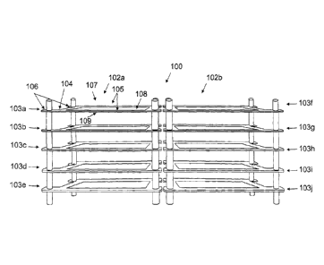
Figure 1 is a perspective view of an embodiment of a carrier according to the
in-
vention, which overall has the reference number 100. The carrier 100 is
designed
for thermal treatment of silicon wafers and is employed, for example, in the
semi-
conductor and photovoltaic industries. Carriers of this type are also known in
Eng-
lish as "stacks".
The carrier 100 has a shelving-like construction that is designed for
receiving sili-
con wafers in a horizontal orientation. The carrier 100 depicted as an example
in
CA 2978448 2017-09-05
- 21 -
Figure 1 comprises two receiving frames 102a, 102b, each of which has five
levels
103a-e and 103f-j for receiving one silicon wafer per level. The total
receiving ca-
pacity of the carrier 100 is ten silicon wafers. In principle, the carrier 100
and the
receiving frames 102a, 102b may be dimensioned such that a desired number of
wafers may be accommodated.
In the carrier 100, the receiving frames 102a, 102b are each embodied in a
single
piece. The carrier is produced completely from a composite material that
compris-
es an amorphous matrix component and an additional component.
The amorphous matrix component is a matrix of silica glass having a chemical
purity of 99.99%; the cristobalite content of the amorphous matrix component
is
0.25%.
In this matrix a phase made of elementary silicon in the shape of non-
spherical
regions is evenly distributed. The additional component has a proportion by
weight
of 2% (m/m). The maximum dimensions of the Si phase regions are on average
(median value) in the range of about 1 pm to 10 pm.
The composite material is gas-tight; it has a density of 2.19 g/cm3 and is
stable in
air up to a temperature of about 1,150 C.
The carrier 100 appears visually translucent to transparent. When viewed under
the microscope, it has no open pores and any closed pores have maximum di-
mensions of on average less than 10 pm. The intercalated Si phase contributes
to
the opacity of the composite material, on the one hand, and has effects on the
optical and thermal properties of the composite material. At high temperatures
the
composite material exhibits high absorption of thermal radiation and high
emissivi-
ty.
In one alternative embodiment (not shown), the entire carrier is embodied in
one
piece; in another alternative embodiment of the carrier 100 (also not shown)
it is
formed from a plurality of substrate support elements. The substrate support
ele-
ments may either be stacked on one another or a holding frame in which the sub-
strate support elements are received may be provided. This has the advantage
that size and receiving capacity may be selected as desired, for example by
suita-
CA 2978448 2017-09-05
- 22 -
bly selecting the holder frame size or the number of substrate support
elements
stacked on one another.
The levels 103a-e and 103f-j are embodied identically; therefore the level
103a is
described in greater detail in the following as an example representing the
levels
103 b-e and 103f-j:
The level 103a has a length of 200 mm (corresponding to the longitudinal side
105
including the projections 106 having a projection length of 30 mm). The width
of
the level 103a is 150 mm (corresponding to the transverse side 104). The thick-
ness of the level 103a is 2 mm.
The level 103a has a top 107 and a bottom 109 opposing the top 107. The top
107 is provided with a depression that acts as a support surface 108 for a
flat
substrate. The support surface 108 has a rectangular shape and has a length of
101 mm and a width of 101 mm.
A conductor path (not shown) is produced on the bottom side 105 by applying
and
firing in a platinum resistance paste. The conductor path is only allocated to
a por-
tion of the bottom side 105; and the conductor path extends across that part
of the
surface of the bottom side 109 that is directly opposite the support surface
108
and the surface area of which corresponds to the support surface 108. The con-
ductor runs in a spiral-shaped line pattern. Clamps (not shown) that permit
the
conductor path to be electrically connected to a current supply (not shown)
are
provided at both ends of the conductor path.
If an electrical potential is applied to the conductor path, the conductor
path heats
up. At the same time, the carrier 100 is heated up in the region of the
support sur-
face 108. From a predetermined temperature the emissivity of the support
surface
108 increases significantly. This may certainly be reasoned by the fact that
the
phase made of elementary silicon that was added to the matrix is a
semiconductor
and by the fact that the energy between valence band and conduction band (band
gap energy) of the semiconductor decreases with temperature, so that if the
tem-
perature and activation energy are high enough, electrons cross from the
valence
band to the conduction band, so that when they return to the valence band
energy
is released in the form of thermal radiation. And the thermally activated
occupation
CA 2978448 2017-09-05
- 23 -
of the conduction band leads to the semiconductor material emitting thermal
radia-
tion in a certain scope for specific wavelengths at room temperature. This
effect is
amplified by high temperatures of the carriers, especially with carrier
temperatures
higher than 600 C. Since the conductor path is arranged opposite the support
sur-
face 108, the support surface 108 can act as a plate-like radiation surface
for
thermal radiation. Some of the emitted thermal radiation is also coupled into
the
carrier 100 so that the latter overall emits thermal radiation. Thermal
radiation es-
pecially in the region of the support surface 108.
In order to be able to direct the emitted thermal radiation onto a substrate
placed
onto the support surface 108, for instance, a reflector layer (not shown) is
also
applied to the conductor path that is applied to the bottom side 105. The
reflector
layer comprises opaque silica glass and has a mean layer thickness of about
1.7
mm. It is characterized by a lack of cracks and a high density of about 2.15
g/cm3;
it is heat resistant up to temperatures higher than 1100 C.
Figure 2 is a sectional depiction of an apparatus according to the invention
for
irradiating semiconductor wafers and is labeled overall with the reference
number
200. The irradiation apparatus 200 has a housing 201 that encloses a process
chamber 202. Arranged in the process chamber 202 is a carrier 203 having two
receiving frames 204a, 204b. A single current feedthrough 220 that is
conducted
through the housing 201 and via which the receiving frames 204a, 204b are at-
tached to a voltage source (not shown) is provided for electrically contacting
the
receiving frames 204a, 204b.
When the same reference numbers are used in Figure 2 than were used in Figure
1, they apply to identical or equivalent components of the carrier as they
were de-
scribed in the foregoing Figure 1.
The carrier 203 is distinguished from the carrier 100 known from Figure 1 in
that it
is embodied in multiple pieces. Substrate support elements 205 that are
inserted
into cylindrical transverse rods 208 via projections 207 disposed on the
transverse
sides 206 are provided for receiving the semiconductor wafers. The transverse
rods 208 are produced from silica glass having a purity of 99.99%. No
additional
component has been added to the silica glass of the transverse rods 208.
CA 2978448 2017-09-05
- 24 -
The transverse rods 208 are provided with slots (not shown) into which one of
the
projections 207 of a support element may be inserted. The slot depth is 7 mm,
the
slot width is 4 mm, and the slot interval is 15 mm. The transverse rods 208
have a
circular radial cross-section, and the diameter of the transverse rods 208 is
20
mm.
The substrate support elements 205 inserted into the transverse rods 208 have
a
length of 200 mm (corresponding to the longitudinal side 210 including the
projec-
tions 207 with a projection length of 30 mm) and a width of 150 mm (correspond-
ing to the transverse side 206). The carrier 203 comprises 40 substrate
support
elements 205 in 20 levels arranged above one another, wherein two substrate
support elements 205 are arranged adjacent to one another in each level.
The substrate support elements 205 are embodied identically. The top side of
each of the substrate support elements has a support surface 212 for receiving
a
semiconductor. The support surface 212 has a width of 101 mm, a length of 101
mm, and a substrate support element height of 2 mm. The substrate support ele-
ments 205 are produced from a laminated glass. The laminated glass comprises
two elements, specifically a first composite element that forms the support
surface
212 and a second composite element that surrounds the support surface 212. The
first composite element comprises silica glass having a purity of 99.99%. The
sec-
ond composite element comprises a composite material that is based on a matrix
of silica glass and to which 3% elementary silicon by weight has been added as
an additional component. A platinum coating that generates heat when current
flows through it is added to the bottom of the support surface 212.
Since only the support surface 212 is produced from the second composite ele-
ment, that is, from the composite material, only the region of the support
surface
212 can emit thermal radiation directly. Certainly the other regions of the
substrate
support element can emit thermal radiation, for instance some radiation that
was
coupled into the substrate support element. However, as a rule such radiation
por-
tions are negligible compared to the total radiant power of the substrate
support
element. In this context, it has proved advantageous when the substrate
support
element has a decoupling zone, for example in the form of a roughened surface,
CA 2978448 2017-09-05
- 25 -
in the region of the transition from the first composite element to the second
com-
posite element. A roughened surface acts as a diffusor and is associated with
a
non-directed and therefore uniform radiation emission. An alternative means
for
reducing the radiant power within the substrate support element is doping the
first
composite component with a thermal radiation-absorbing doping agent.
Figure 3 depicts two views (I, II) of a substrate support element 300 of the
inven-
tion.
View I provides a perspective elevation of the top side (A) of the substrate
support
element 300; View II depicts the bottom side (B) of the substrate support
element
300.
The substrate support element 300 is produced from two materials, specifically
it
is made of silica glass in the region 310 surrounding the support surface 304
and
it is made of a composite material in the region of the support surface 304.
The
composite material comprises a matrix made of silica glass. The matrix appears
visually translucent to transparent. When viewed under the microscope, it has
no
open pores and any closed pores have maximum dimensions of on average less
than 10 pm. A phase made of elementary silicon in the shape of non-spherical
regions is evenly distributed in this matrix. The proportion by weight of the
phase
made of elementary silicon is 5%. The maximum dimensions of the Si phase re-
gions are on average (median value) in the range of about 1 pm to 10 pm. The
composite material is gas-tight; it has a density of 2.19 g/cm3 and is stable
in air
up to a temperature of about 1200 C.
The intercalated Si phase contributes overall to the opacity of the composite
mate-
rial, on the one hand, and has effects on the optical and thermal properties
of the
composite material. At high temperatures the composite material exhibits high
ab-
sorption of thermal radiation and high emittance.
The emissivity of the composite material is measured at room temperature using
an integrating sphere (also known as Ulbricht sphere). The Ulbricht sphere per-
mits measurement of the directional hemispherical spectral reflectance Rol and
of
the directional hemispherical spectral transmittance Tgh, from which the
normal
CA 2978448 2017-09-05
- 26 -
spectral emissivity is calculated. Using the aforesaid õBlack-Body Boundary
Condi-
tions" (BBC) measurement principle, the emissivity is measured at an elevated
temperature in the wavelength range of 2 to 18 pm by means of an FTIR spec-
trometer (Bruker IFS 66v Fourier Transform Infrarot (FTIR)) to which a BBC sam-
ple chamber is coupled via an additional optical system. This sample chamber,
in
the half-spaces in front of and behind the sample mount, has temperature-
controllable black-body environments and a beam exit opening with detector.
The
sample is heated to a predetermined temperature in a separate oven, and for
the
measurement it is moved into the beam path of the sample chamber with the
black body environments set to the predetermined temperature. The intensity
cap-
tured by the detector is composed of an emission component, a reflection compo-
nent and a transmission component ¨ that is, of intensity emitted by the
sample
itself, intensity impinging on the sample from the front half-space and
reflected by
said sample, and intensity which impinges on the sample from the rear half-
space
and is transmitted by said sample. Three measurements must be carried out in
order to determine the individual parameters of emissivity, reflectance, and
trans-
mittance.
The emissivity measured on the composite material in the wavelength range from
2 pm to about 4 pm depends on the temperature. The higher the temperature is,
the higher the emission is. At 600 C, the normal emittance in the wavelength
range of 2 pm to 4 pm is greater than 0.6. At 1000 C, the normal emittance in
the
entire wavelength range between 2 pm and 8 pm is greater than 0.75.
The substrate support element 300 has two longitudinal sides 301a, 301b and
two
transverse sides 302a, 302b. Disposed on each of the transverse sides 302a,
302b are two projections 303 with which the substrate support element 300 may
be attached to the transverse rods of a holding frame (not shown).
The substrate support element 300 has a length of 300 mm (corresponding to the
longitudinal sides 301a and 301b including each projection 303 having a projec-
tion length of 30 mm) and a width of 200 mm (corresponding to the transverse
side 302a, 302b). The thickness of the substrate support element 300 is 4 mm.
CA 2978448 2017-09-05
- 27 -
A support surface 304 in the shape of a rectangular depression is provided for
a
semiconductor on the top (A) of the substrate support element 300. The support
surface 304 has a rectangular shape and has a length of 121 mm and a width of
121 mm. The support surface 304 acts both as a support surface for a substrate
and as a radiating surface for thermal radiation. The direction of radiation
is indi-
cated by the directional arrow 308.
A conductor path 305 that is produced from a platinum resistance paste is
applied
to the top surface of the bottom side (B). The conductor path 305 has a
meander-
ing course. Contacts 306 for supplying electrical energy are welded to each
end of
the conductor path 305. The conductor path 305 runs within a surface area 307
that corresponds to the support surface 304. The distance between adjacent con-
ductor path segments is 2 mm. The conductor path 305 has a cross-sectional ar-
ea of at least 0.02 mm2 with a width of 1 mm and a thickness of 20 pm. Because
of the thin thickness, the material portion of the expensive conductor path
material
is low compared to its efficiency. The conductor path 305 has direct contact
with
the bottom side of the substrate support element 300, so that the greatest
possi-
ble amount of heat is transferred into the substrate support element 300.
Both the support surface 307 and the conductor path 305 are covered by a
reflector
layer (not shown) made of opaque silica glass. The reflector layer has a mean
layer thickness of 1.7 mm. It is characterized by a high density of about 2.15
g/cm3.
In addition, it is thermally resistant up to temperatures higher than 1100 C.
The
reflector layer completely covers the conductor 305 and thus protects it from
chemical and mechanical influences from the environment Moreover, it reflects
radiation emitted by the substrate support element in the direction of the
bottom
side and reflects said radiation back towards any substrate that has been
placed
onto the support surface 304.
Figure 4 is a top view of the bottom side 401 of an alternative embodiment of
a
substrate support element 400.
The substrate support element 400 is produced completely from a composite ma-
terial, the matrix component of which is silica glass, wherein a phase made of
el-
ementary silicon is added to the silica glass at a concentration of 3%.
CA 2978448 2018-12-07
- 28 -
A conductor path 402 made of a silver paste is printed onto the bottom side
401
and fired. The conductor path 402 has a meandering course in which the curved
areas are sharply tapered. This has the advantage that, in contrast to a round
curve path, the edge regions of the substrate support element have a lower
cover-
ing density of the conductor path. This ensures that the edge regions are not
heated excessively during operation compared to the center region of the sub-
strate support element 400. The shape of the conductor path thus contributes
to
the most uniform possible radiation of any substrate positioned on the top.
Moreo-
ver, no reflector has been applied to the bottom side 401, in particular to
the con-
ductor 402, so that radiation emitted in the region of the bottom side 401 is
availa-
ble for irradiating an adjacent substrate disposed therebelow.
Figure 5 is a top view of the bottom of an inventive substrate support element
having the overall reference number 500. Applied to the bottom side and corre-
sponding to the support surface, are two conductor paths 501, 502 made of
plati-
num, and an electrical voltage may be applied to each individually. Since the
con-
ductor paths 501, 502 are individually electrically controllable, that is,
they may be
operated with different operating voltages or operating currents, a desired
temper-
ature distribution on the substrate to be heated may be set simply and rapidly
by
appropriately selecting the operating voltages or operating currents.
Figure 6 is a top view of the bottom side of a fourth embodiment of a
substrate
support element 600 of the invention. The substrate support element 600 com-
prises two conductor paths 601, 602, each of which is individually
electrically con-
trollable.
It has been found that during thermal substrate treatment the edge regions of
the
substrate are frequently heated more intensely than the center region thereof.
The
most uniform possible temperature distribution is attained on the substrate to
be
heated in that the conductor paths that may be operated independently from one
another with different operating currents or operating voltages are allocated
to the
edge region and to the center region. In Figure 6, the conductor path 602 is
allo-
cated to the substrate edge region and conductor path 601 is allocated to the
sub-
strate center region. It is possible to attain uniform irradiation of the
substrate by
CA 2978448 2017-09-05
- 29 -
varying the operating currents or operating voltages applied to the conductor
paths 601, 602.
CA 2978448 2017-09-05