Note: Descriptions are shown in the official language in which they were submitted.
CONNECTABLE SMART LABEL OR TAG, AND METHODS OF MAKING AND
CONNECTING THE SAME
FIELD OF THE INVENTION
[0002] The present invention generally relates to the field(s) of product
security and
authentication. More specifically, embodiments of the present invention
pertain to an electronic
tag and/or device (which may communicate wirelessly) that is connectable to
one or more
additional components, such as an antenna, sensor, battery, display and/or
switch, and methods
of manufacturing, connecting, and using the same.
DISCUSSION OF THE BACKGROUND
[0003] Wireless communication tags, such as the OpenSense security tags
commercially
available from Thin Film Electronics ASA, include labels with electronics
printed or otherwise
formed thereon that detect whether a bottle or package has been opened and
communicate the
continuity state are NFC (near field communication) or RF (radio frequency)
protocols. This
product is being evaluated and accepted for instance in the packaging
industry.
[0004] In the packaging industry, there are thousands of different package
types.
However, on a commercial scale, it is difficult or impossible to tailor a
different wireless
communication tag for each different type, shape and size of package.
Furthermore, current
solutions generally protect only one interface (e.g., one side of a package
such as a carton),
which is insufficient for many applications, such as packaging types with more
than one
interface between separable parts (e.g., a box with separable flaps on the top
and bottom).
- 1 -
CA 2979367 2017-09-18
[0005] Printing items such as artwork or text on containers such as cartons
has been long
known. However, high-speed printing of electrical structures such as antennas
on packaging
such as cartons has only relatively recently become possible.
[0006] A challenge facing the packaging industry is finding a shape for a
sense line or
other security feature that protects each opening of the package. For example,
a package such as
a box or carton typically has at least 2-3 openings at the interfaces between
separable parts. The
challenge to do so at high speed is even greater.
[0007] WO 2016/066925 discloses an anti-counterfeiting NFC device to ensure
the
authenticity of the contents of a bottle. The hybrid NFC tag of WO 2016/066925
includes
components on a plastic substrate and a paper-based substrate, coupled to each
other by a
transformer formed by a first winding arranged on the plastic substrate and a
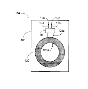
second winding
arranged on the paper-based substrate. The paper-based substrate may typically
be in strip form
and include a sacrificial zone through conductive tracks connecting the
components of the paper-
based substrate. The paper-based substrate may comprise a driver microcircuit
connected to the
second winding, and the plastic substrate may comprise an antenna coil
connected to the first
winding. The paper-based substrate may comprise an impedance connected to the
second
winding by a conductor track crossing the sacrificial area, and the plastic
substrate may include a
driver microcircuit and an antenna coil connected to the first winding. The
impedance may be a
short circuit. The driver microcircuit can be configured to be powered by the
antenna coil and
include functions for transmitting information and cryptographic functions,
the components of
the NFC tag being chosen so that the rupture of the sacrificial area lowers
the power supply
received by the microcircuit to a level insufficient to supply cryptographic
functions, but at a still
sufficient level to power the transmission functions. However, loss of
additional functionality
such as cryptographic functions is undesirable in many security and/or
identification devices, and
there is a need for a security and/or identification device that retains full
functionality at all times
while still ensuring the authenticity of the contents of the package or
container to which the
security and/or identification device is attached, affixed and/or associated.
- 2 -
CA 2979367 2017-09-18
[0008] This "Discussion of the Background" section is provided for
background
information only. The statements in this "Discussion of the Background" are
not an admission
that the subject matter disclosed in this "Discussion of the Background"
section constitutes prior
art to the present disclosure, and no part of this "Discussion of the
Background" section may be
used as an admission that any part of this application, including this
"Discussion of the
Background" section, constitutes prior art to the present disclosure.
SUMMARY OF THE INVENTION
[0009] There is a need for a generic, standard or universal security or ID
tag or device
that facilitates or enables sensing the continuity state of a package or
container having 2 or more
interfaces between separable parts of the package or container, and that can
be attached to
packages at high speed. Thus, the present invention generally relates to the
field(s) of product
security and authentication. More specifically, the present invention relates
to a standard
communication device (e.g., a wireless or battery-operated security tag) with
two open circuit
endpoints (e.g., connection terminals), and methods of manufacturing and using
such devices
(e.g., attaching the circuit endpoints to a sense line that may be printed on
a container or product
packaging).
[0010] Thus, in one aspect, the present invention relates to an electronic
security and/or
identification (ID) tag and/or device. The tag and/or device may communicate
wirelessly, or
alternatively, may include a display. The present security and/or ID tag
and/or device includes a
first substrate, an integrated circuit on the substrate, and a component
selected from an antenna
and a battery on the same substrate or a different substrate. The first
substrate is configured to be
applied, affixed or attached to a package or container. The integrated circuit
includes (i) a first
set of connection pads electrically connected to the integrated circuit and
configured to be
electrically connected to another component external to the integrated circuit
and the first
substrate, and (ii) a memory storing a unique identification number for the
security and/or
identification device. The antenna is configured to (i) receive a first
wireless signal and
optionally transmit or broadcast a second wireless signal and (ii) enable the
integrated circuit to
- 3 -
CA 2979367 2017-09-18
extract power from the first wireless signal. The battery provides power to
the integrated circuit.
The present security and/or identification device may further comprise an
adhesive on the
substrate (e.g., for securing or affixing the integrated circuit to the
package or container).
[0011] In exemplary embodiments, the integrated circuit comprises a
continuity sensor
electrically connected to the first set of connection pads, configured to
determine a continuity
state of the package or container. In such embodiments, the memory generally
includes one or
more bits configured to store a value corresponding to the continuity state of
the container or
package. In further embodiments, the integrated circuit may comprise one or
more additional
sets of connection pads electrically connected to the integrated circuit, and
the combined first set
of connection pads and additional set(s) of connection pads are configured to
be electrically
connected to a plurality of sensing lines on the package or container.
[0012] In various embodiments of the present security and/or
identification device, the
component comprises the antenna. In one case, the antenna is on a common
substrate (e.g., the
same substrate as the integrated circuit). In such a case, the security and/or
identification device
may further comprise a strap electrically connecting an inner end of the
antenna to a location on
the substrate external to the antenna.
[0013] In another case, the antenna is on a different substrate from the
integrated circuit.
In such a case, the antenna may include a second set of connection pads, and
the integrated
circuit includes first and second bond pads configured to be electrically
connected to the second
set of connection pads. In this manner, the integrated circuit functions as a
strap, electrical
bridge or other electrical connection connecting the inner and outer ends of
the antenna. Such a
configuration also enables the antenna to consist of a single metal layer.
[0014] In some embodiments of the present security and/or identification
device,
invention, the component comprises the battery. In further embodiments, the
security and/or
identification device further comprises a display on the same or different
substrate as the battery
and/or integrated circuit. In some embodiments, the battery and the display
are on a common
- 4 -
CA 2979367 2017-09-18
substrate. The display is typically electrically connected to both the battery
and the integrated
circuit. The integrated circuit may be configured to provide data and/or one
or more instructions
to the display.
[0015] Various embodiments of the present security and/or identification
device may
further comprise a further component, such as a switch or a sensor other than
a continuity sensor,
on the same or different substrate as the integrated circuit and/or the
antenna or battery. In
general, the further component is electrically connected to the integrated
circuit. When the third
component is on a substrate other than the integrated circuit substrate, the
integrated circuit
comprises a set of unique connection pads to be electrically connected to the
further component.
[0016] When the security and/or identification device includes an antenna
(and thus is
able to communicate wirelessly), the device may be a near field and/or radio
frequency (RF)
security and/or identification device.
[0017] In various embodiments, the integrated circuit includes one or more
printed layers
and/or one or more thin films. In further embodiments, the integrated circuit
may comprise a
plurality of printed layers. For example, the integrated circuit may comprise
one or more printed
layers and one or more thin films.
[0018] In additional or alternative embodiments, the substrate(s) on which
the integrated
circuit, the antenna, the battery and//or the further component are formed may
comprise a plastic
or a metal foil. In some embodiments, the substrate is flexible and/or can
withstand a processing
temperature of up to 200 C.
[0019] In another aspect, the present invention relates to a method of
manufacturing a
security and/or identification device, comprising forming an integrated
circuit on a first substrate
configured to be applied, affixed or attached to a package or container, and
forming an antenna
or a battery on the first substrate or a second substrate. As for the present
device or tag, the
integrated circuit includes (i) a first set of connection pads electrically
connected to the
- 5 -
CA 2979367 2017-09-18
integrated circuit and configured to be electrically connected to a component
external to the
integrated circuit and the first substrate, and (ii) a memory storing a unique
identification number
for the security and/or identification device. The antenna is configured to
(i) receive a first
wireless signal and optionally transmit or broadcast a second wireless signal
and (ii) enable the
integrated circuit to extract power from the first wireless signal, and the
battery provides power
to the integrated circuit.
[0020] In some embodiments of the present method, the integrated circuit
comprises a
continuity sensor electrically connected to the first set of connection pads,
configured to
determine a continuity state of the package or container. In such embodiments,
the memory may
include one or more bits configured to store a value corresponding to the
continuity state of the
container or package. Furthermore, forming the integrated circuit may comprise
forming one or
more additional sets of connection pads electrically connected to the
integrated circuit and
configured to be electrically connected to a plurality of sensing lines on the
package or container.
[00211 In various embodiments of the present method, the security and/or
identification
device comprises the antenna. Thus, the present method may comprise forming
the antenna on
the first substrate (i.e., the same substrate as the integrated circuit). In
such embodiments, the
method may further comprise forming a strap electrically connecting an inner
end of the antenna
to a location on the first substrate external to the antenna.
[0022] Alternatively, the method may comprise forming the antenna on the
second (i.e., a
different) substrate. In such embodiments, forming the antenna may include
forming a second
set of connection pads on the second substrate, and individual ones of the
second set of
connection pads may be electrically connected to inner and outer ends of the
antenna,
respectively. As a result, forming the integrated circuit may include forming
first and second
bond pads (e.g., in an uppermost or lowermost layer of metallization)
configured to be
electrically connected to the second set of connection pads. Similar to the
present security and/or
identification device, in such a configuration, the integrated circuit
functions as a strap
connecting the inner end of the antenna and the outer end of the antenna. In
addition, the
- 6 -
CA 2979367 2017-09-18
antenna can consist of a single metal layer, and forming the antenna may
consist of forming a
metal layer on the substrate, and etching the metal layer to form the antenna.
Alternatively,
forming the antenna may comprise printing a metal ink on the substrate in a
pattern
corresponding to the antenna.
[0023] In other embodiments of the present method, the security and/or
identification
device comprises the battery. Such embodiments may further comprise forming a
display on the
first substrate, the second substrate or a third substrate. The display is
electrically connected to
the battery and the integrated circuit, and the integrated circuit is
generally configured to provide
data and/or one or more instructions to the display. In one example, the
method comprises
forming the battery and the display on a common substrate.
[00241 In further embodiments of the present method, forming the display
may comprise
forming a photoactive layer on the same or different substrate, and forming a
plurality of
electrodes thereto (at least one of which may be transparent). When the
photoactive layer and
the electrodes are not formed on a transparent substrate (or transparent
window in the substrate),
the method may further comprise forming a transparent window over the
photoactive layer and
the electrodes. In addition, forming the battery may comprise forming a first
current collector
layer, a cathode or anode thereon, an electrolyte layer on the cathode or
anode, the other of the
cathode or anode on the electrolyte layer, and a second current collector
layer on the other of the
cathode or anode. The layers of the battery may be formed by printing and/or
thin film
processing.
[0025] In various embodiments of the present method, the method further
comprises
depositing an adhesive on the first substrate and/or forming a switch and/or a
sensor (other than
the continuity sensor) on the first substrate, the second substrate or a third
substrate. The switch
and/or other sensor is electrically connected to the integrated circuit. In
some examples, the
method comprises forming the switch and/or other sensor on a substrate other
than the first
substrate, in which case the method may further comprise forming a second set
of connection
- 7 -
CA 2979367 2017-09-18
pads electrically connected to the integrated circuit and configured to be
electrically connected to
the third external component.
[0026] In other or further embodiments of the present method, forming the
integrated
circuit comprises printing one or more layers of the integrated circuit. For
example, forming the
integrated circuit may comprises printing a plurality of layers of the
integrated circuit.
Additionally or alternatively, the method may further comprise forming one or
more additional
layers of the integrated circuit by thin film processing. In one embodiment,
forming the
integrated circuit comprises printing all of the layers of the integrated
circuit. In other
embodiments, forming the integrated circuit comprises printing one or more
layers of the
integrated circuit and forming the remaining layers of the integrated circuit
by thin film
processing.
[0027] As for the present security and/or identification device, the first
substrate (as well
as the second and/or third substrate[s]) in the present method may comprise a
plastic or a metal
foil. For example, the first substrate may be flexible and may withstand a
processing
temperature of up to 200 C.
[0028] In a further aspect, the present invention relates to a package or
container
including first and second separable parts with an interface between the
separable parts, with the
security and/or identification device discussed above thereon. The integrated
circuit and the
antenna or battery are on one of the first and second separable parts of the
package or container.
In addition, a sensing line is on the first and second separable parts of the
package or container
and in or over an interface between the first and second separable parts. The
package or
container may comprise a box, a tray with a lid, a bottle, an envelope or a
bag.
[0029] In various embodiments, the package or container comprises multiple
sealed or
closed compartments, the integrated circuit comprises a plurality of sets of
connection pads, the
sensing line comprises a plurality of the sensing lines, and each of the
plurality of sensing lines
extends over a unique one of the multiple sealed or closed compartments.
- 8 -
CA 2979367 2017-09-18
[0030] In an even further aspect, the present invention relates to a method
of determining
a continuity state of a package or container that includes connecting
connection pads of an
integrated circuit on a substrate (as described herein) to a sensing line on
first and second
separable parts of the package or container and over an interface between
first and second
separable parts of the package or container, and sensing the continuity state
of the package or
container using the integrated circuit and a continuity sensor therein. The
integrated circuit may
be electrically connected to an antenna or a battery. The sensing line is
configured to sense or
determine a continuity state of a package or container on which the security
and/or identification
device is placed or to which the security device is fixed or adhered.
[0031] In various embodiments, placing the integrated circuit on the
container or package
includes adhering or affixing the integrated circuit to the container or
package. For example,
adhering the integrated circuit to the container or package may include
applying an adhesive on
the substrate on which the integrated circuit is formed, and pressing the
substrate to the container
or package.
[0032] The present invention advantageously enables a manufacturer of
integrated
circuits for sensing a continuity state of a package or container to make
and/or manage a reduced
number of products, and enables a packager to electronically protect any size
or shape of carton,
container or other packaging. This reduces the lead time for providing
packaged products to a
customer since a standard and/or uniformly-sized integrated circuit and power
supply source
(e.g., antenna or battery) can be stocked by the packager, and reduces the
cost and complexity of
designing a new integrated circuit and power supply source for each size
and/or shape of
container. These and other advantages of the present invention will become
readily apparent
from the detailed description of various embodiments below.
BRIEF DESCRIPTION OF THE DRAWINGS
[0033] FIG. 1 shows an exemplary wireless security tag in accordance with
one or more
embodiments of the present invention.
- 9 -
CA 2979367 2017-09-18
[0034] FIGS. 2A-B show an alternative exemplary wireless security tag in
accordance
with one or more embodiments of the present invention.
[0035] FIGS. 3A-B show an exemplary connection between connection pads of
the
wireless security tag of FIGS. 1-2 and terminals of a printed sense line on a
different substrate in
accordance with one or more embodiments of the present invention.
[0036] FIGS. 4A-C show an exemplary security tag connected to a customized
sensing
line on a package or container in accordance with one or more embodiments of
the present
invention.
[0037] FIGS. 5A-C show an exemplary multi-compartment container having an
alternative security tag with multiple continuity sensors therein in
accordance with one or more
alternative embodiments of the present invention.
[0038] FIG. 6 shows exemplary functional modules or units for the present
security or ID
tag or device in accordance with embodiments of the present invention.
[0039] FIGS. 7A-B show an exemplary security and/or ID tag or device with
a display in
accordance with one or more embodiments of the present invention.
[0040] FIG. 8 shows an exemplary integrated circuit for use in the present
wireless
security or ID tag or device.
[0041] FIG. 9 shows a flow chart for an exemplary method of manufacturing
and
optionally using the present security and/or ID device in accordance with one
or more
embodiments of the present invention.
- 10 -
CA 2979367 2017-09-18
DETAILED DESCRIPTION
[0042] Reference will now be made in detail to various embodiments of the
invention,
examples of which are illustrated in the accompanying drawings. While the
invention will be
described in conjunction with the following embodiments, it will be understood
that the
descriptions are not intended to limit the invention to these embodiments. On
the contrary, the
invention is intended to cover alternatives, modifications and equivalents
that may be included
within the scope of the invention. Furthermore, in the following detailed
description, numerous
specific details are set forth in order to provide a thorough understanding of
the present
invention. However, it will be readily apparent to one skilled in the art that
the present invention
may be practiced without these specific details. In other instances, well-
known methods,
procedures and components have not been described in detail so as not to
unnecessarily obscure
aspects of the present invention. Furthermore, it should be understood that
the possible
permutations and combinations described herein are not meant to limit the
invention.
Specifically, variations that are not inconsistent may be mixed and matched as
desired.
[0043] In addition, for convenience and simplicity, the terms "part,"
"portion," and
"region" may be used interchangeably but these terms are also generally given
their art-
recognized meanings. Also, unless indicated otherwise from the context of its
use herein, the
terms "known," "fixed," "given," "certain" and "predetermined" generally refer
to a value,
quantity, parameter, constraint, condition, state, process, procedure, method,
practice, or
combination thereof that is, in theory, variable, but is typically set in
advance and not varied
thereafter when in use.
[0044] The present wireless security or ID device is produced without sense
lines, as
shown in FIG. 1. The wireless security or ID device is then coupled to a
printed sense loop on
the container or package, which means that it can be used for almost any type
of package without
modification. However, there is a need to create an ohmic contact to
electrically connect the
printed sense loop and the antenna and/or integrated circuit. This is a
challenge that can be
solved in several ways.
- 11 -
CA 2979367 2017-09-18
[0045] One objective of the present invention is to connect a wireless
security device to a
printed sense loop. Some commercially-available wireless security devices
include an antenna
made of aluminum. One challenge is that aluminum oxidizes rapidly, which makes
it hard to
create an ohmic contact between the connection points of the antenna and the
printed sense loop.
One solution is to use a conductive ink or adhesive to attach the antenna
and/or integrated circuit
of the wireless security device to the printed sense line, and sinter it with
a laser as shown in
FIGS. 3A-B. Another solution is to use different antenna materials that do not
oxidize easily
(e.g., copper, graphene, etc.). A third solution is to protect the aluminum
antenna or connection
point (terminal) using a protective coating or similar oxygen barrier.
[0046] One way to implement the present wireless security device in
packages and
containers is to attach the antenna and/or integrated circuit to the sense
line in a packaging
process / manufacturing line using a conductive glue, laser welding or similar
attachment
technique. The printed loop that detects the continuity state of the package
(e.g., whether the
package is opened or sealed) can typically be printed using a conductive ink
(e.g., silver or other
metal, carbon, a conductive polymer, etc.). Another objective is to use
sensors in or in proximity
to the conductive sense loop, thus using sensor data to indicate an opened
package or container
instead of a physical tear action (e.g., a broken sense line).
Exemplary Connectable Security Tags with a Wireless Communication Device
and a Continuity Sensor thereon
[0047] The present invention relates to an electronic security tag and/or
device with a
sensor configured to detect an opened or tampered state of a package or
container to which the
tag and/or device is attached. In one embodiment, the security tag or device
communicates
wirelessly (e.g., with an NFC or RF reader). In other embodiments, the
security tag or device
includes a display and a battery. The security device generally includes an
integrated circuit on
or over a substrate, an antenna or display on the same or a different
substrate, and a first set of
terminals electrically connected to the integrated circuit (and, optionally,
the antenna or display).
The first set of terminals is configured to be electrically connected to a
sense line or loop on a
package or container. The antenna is configured to receive a first wireless
signal (e.g., from the
- 12 -
CA 2979367 2017-09-18
reader) and/or transmit or broadcast a second wireless signal (e.g., from the
integrated circuit).
The display is configured to display an indicator indicating a continuity
state of a package or
container on which the security device is placed or to which the security
device is fixed or
adhered. The integrated circuit is configured to determine a continuity state
of the package or
container and either (i) process the first wireless signal and/or information
therefrom and
generate the second wireless signal and/or information therefor, or (ii)
indicate the continuity
state of the package or container using the display. A receiver and/or
transmitter may be
integrated into the integrated circuit (e.g., when the security device
includes an antenna).
[0048] Thus, the security device is connectable to a sensing line on the
package or
container. The sensing line is generally configured to sense a continuity
state of the package or
container on or in which the sensing line has been formed (e.g., printed). In
one embodiment,
the integrated circuit includes a first set of terminals to which the sensing
line is connected. The
first set of terminals is different from a second set of terminals that are
electrically connected to
the antenna or display. In an alternative embodiment, the antenna is also
electrically connected
to the first set of terminals.
[0049] In some embodiments, the present tag and/or device is a generic
wireless security
tag with a generic antenna connected thereto, and a mechanism for connecting
the generic
wireless security tag to a continuity sensor on a separate substrate (e.g.,
the package or
container). However, the invention is not so limited. Connecting the generic
OS tag to a
continuity sensor is one of several possible components that can be made more
easily or
efficiently on a separate substrate. Displays, additional sensors, batteries,
and switches (e.g., to
connect/disconnect the tag and/or device to another component) can be
connected in the same
way (e.g., using a set of terminals electrically connected to an integrated
circuit).
[0050] In fact, the antenna may also be separately connectable to the
integrated circuit
(generally through a second set of terminals different from the first set of
terminals). However,
in some embodiments, at least one of the separately connectable components is
on the same
substrate as the integrated circuit (the antenna is preferred, in typical
embodiments). The
- 13 -
=
CA 2979367 2017-09-18
separately connectable component may be electrically connected to the
integrated circuit and/or
antenna using any of a variety of different mechanisms (e.g., capacitive,
inductive, and several
different kinds of ohmic connections).
[0051] Thus, in one aspect, the present invention relates to a generic,
standard or
universal security tag including an integrated circuit (IC) and a second
component (generally
either [1] an antenna or [2] a battery and an optional display) on one
substrate, with a set of
terminals configured to electrically connect the IC to a third component on a
different substrate.
In a second aspect, the present invention relates to a generic, standard or
universal security tag on
a first substrate with a plurality of sets of terminals, each connected to a
functionally different
component on a plurality of different substrates. In this aspect, at least one
of the different
components is an antenna or battery, and another is a sensor, display, or
switch.
[0052] In any case, the present invention provides a fully secure wireless
or display-
based security solution for any shape of package, container or carton. The
solution does not
require line of sight, so it does not interfere with any graphics on the
package, container or
carton. The present security tag/device can assist with use cases such as
return fraud, in-store
tampering of cartons, and consumer protection. The present security tag/device
can also help
with consumer engagement (e.g., to ensure that the consumer opens the package,
container or
carton correctly). Some commercially available devices offering a 2-state
solution do not always
work if the container or package is not opened as intended by the manufacturer
or packager.
[0053] The present invention is also applicable to flexible packaging.
Thus, in various
embodiments, the antenna and/or the integrated circuit can be on a substrate
that comprises
paper, a glass/polymer laminate, a paper/polymer laminate, a high temperature
polymer, a metal
foil, or a combination thereof. When the substrate comprises the high
temperature polymer, the
high temperature polymer may comprise a polyimide, a polyethersulfone, a
polyethylene
naphthalate (PEN), or a polyether ether ketone (PEEK). Alternatively, when the
substrate
comprises a metal foil, the metal foil may comprise aluminum, stainless steel
or copper.
- 14 -
CA 2979367 2017-09-18
[0054] In summary, the present invention comprises a security and/or
identification tag
(e.g., an inlay and/or chip) with a decoupled sense line, on different
substrates and/or materials.
The present invention allows the packager to create the sense line in any way
that makes sense
(e.g., printing on any of a variety of substrates with any of a variety of
materials by any of a
variety of techniques).
[0055] The sense line in the present security device and/or tag is
effectively made with an
open circuit. The circuit endpoints can be printed with a wide pad (for ease
of placement
tolerance) and optionally a via hole, and in some cases with isotropic or
anisotropic conductive
adhesive on the underside that can be pattern-printed. The via functions as a
conduit connecting
the integrated circuit to the printed sense trace(s) or line(s). The sense
line can be printed over
all of the openings of the container (e.g., the three interfaces or openings
in a carton), so any side
of the carton that is opened changes the state of the continuity sensor and
indicates an open
package. This type of via or through-hole construction is common in the
printing/die cutting
industry, but to the best of the inventors' knowledge, it has not been used to
attach a wireless or
display-based security tag to a printed sense line.
[0056] For example, attachment of the terminals connected to the IC could
be made with
an anisotropic pressure-sensitive adhesive (PSA) and/or a heat-activated
conductive adhesive
(e.g., that electrically connects the sense lines to the terminals when
heating a shrink-wrap film
applied to the package or container). Alternatively, the sense line may be
coupled to the IC
using a capacitive coupling approach (e.g., an inductor printed over an
interface of the container
that is also capacitively coupled to the antenna of the present security
tag/device). The present
security tag/device has the potential to help the sense line to break more
efficiently and/or
effectively on the container, and makes both processes (printing on the
container and inlay/tag
manufacturing) more efficient.
[0057] FIG. 1 shows an exemplary wireless security tag/device 100,
including an
integrated circuit (IC) 110, an antenna 120, antenna terminals 125a-b, and IC
terminals 130 and
132 on a substrate 105. Traces 134 and 136 electrically connect the IC
terminals 130 and 132 to
- 15 -
CA 2979367 2017-09-18
the IC 110 (e.g., to pads on the IC 110). The antenna terminals 125a-b are for
a strap to
electrically connect the inner end of the antenna 120 to a location outside
the antenna 120.
[0058] The substrate 105 for the wireless security tag/device 100 of FIG. 1
is rectangular
or substantially rectangular, although the substrate 105 may have another
shape suitable for a
particular application (e.g., such as t-shaped, oval, elongated, rectangular
or other quadrilateral
[with or without rounded corners], tapered, or as otherwise described herein).
In exemplary
embodiments, the substrate 105 may comprise paper, a polymer (e.g., a high
temperature
polymer such as polyethylene naphthalate [PEN] or polyethylene terephthalate
[PET], nylon,
polyvinyl alcohol and copolymers thereof [e.g., ethylene-vinyl alcohol (EVOH)
copolymers],
polyvinyl chloride [PVC], polypropylene [PP], polychlorotrifluoroethylene
[PCFE; e.g.,
ACLAR pharmaceutical packaging film, available commercially from Honeywell],
polyethylene [PE; e.g., high density PE (HDPE)]), a metal layer or foil (e.g.,
comprising
aluminum, stainless steel or copper), a laminate or other combination thereof,
etc.
[0059] In exemplary embodiments, the integrated circuit 110 includes a
continuity sensor
(not shown) electrically connected to the traces 134 and 136. The integrated
circuit 110 may
further include a memory (not shown) including one or more bits configured to
store a value
corresponding to a continuity state of a container or package on which the
substrate 105 is
attached or secured. The memory may also include a plurality of bits that
store identification
information (e.g., a device identification number), product information,
information from at least
one other sensor, software instructions, etc.
[0060] In some embodiments, the integrated circuit 110 includes one or more
printed
layers. For example, memory bits storing information that does not change
(e.g., device
identification information, instructions) may be formed by printing one or
more layers of the
memory, similar to a read-only memory (ROM). In one example, the integrated
circuit is an
"all-printed" integrated circuit (i.e., all or substantially all layers are
printed layers). In further
embodiments, the integrated circuit 110 includes one or more thin films, as an
alternative to or in
- 16 -
CA 2979367 2017-09-18
combination with one or more printed layer(s). In any of these embodiments,
the IC 110 can be
formed directly on the substrate 105.
[0061] In various embodiments, the antenna 120 may comprise a coil,
concentric rings or
a plurality of loops or "rings" in a spiral. For example, the number of loop
or "rings" may be
from 2 to about 50, or any natural number or range of natural numbers therein.
Alternatively, the
shape of the antenna 120 may be a square, rectangular, oval or serpentine, and
may have
dimensions that match any of multiple form factors, while preserving
compatibility with reader
hardware (e.g., the NFC 13.56 MHz target frequency). The antenna 120 may be
printed (e.g.,
using a printed conductor such as, but not limited to, silver from a silver
paste or ink) or formed
using conventional methods such as blanket deposition and etching (e.g., by
sputtering or
evaporating aluminum on the substrate 105 and patterning by low-resolution
[e.g., 10-1,000 }tm
line width] photolithography and wet or dry etching).
[0062] In one embodiment, the IC 110 is formed on ends of the traces 134
and 136, the
outer end of the antenna 120, and the trace to which the antenna pad 125b is
connected.
Alternatively, the IC 110 is built up layer by layer on the substrate 105, and
the ends of the traces
134 and 136, the outer end of the antenna 120, and the trace to which the
antenna pad 125b is
connected are formed in contact with conductive pads on the IC 110 that are,
in turn, connected
to circuitry in the IC 110.
[0063] The inner end of the antenna 120 may be electrically connected to a
first pad
125a, which is conventionally connected to a second pad 125b that is
electrically connected to a
terminal on the integrated circuit 130. In one example, a strap is formed on
the underside of the
substrate 105 and bonded to the pads 125a-b through vias in the substrate.
Alternatively, the
strap can be formed on an interposer (i.e., an insulating substrate) and
bonded to the pads 125a-b
through vias in the interposer or in a dielectric layer formed over the strap.
[0064] In the alternative shown in FIGS. 2A-B, the integrated circuit 110'
can function as
such a strap when formed on an electrically insulating interposer (a so-called
"integrated
- 17 -
CA 2979367 2017-09-18
interposer"). In such embodiments, the integrated circuit 110' includes first
and second pads
112a-b (that connect to antenna pads 125a-b) and third and fourth pads 114a-b
(that connect to
pads 131 and 133 at the ends of traces 134 and 136 on the substrate 105').
With the exception of
antenna pad 125a being on the inside of the antenna 120' and antenna pad 125b
being on the
outside of the antenna 120, the various pads may be in any location as long as
the first and
second pads 112a-b overlap with the antenna pads 125a-b, and the third and
fourth pads 114a-b
overlap with the trace pads 131 and 133. FIG. 2B shows the IC 110 electrically
connected to the
antenna 120' and the traces 134 and 136 through the first and second pads 112a-
b and the third
and fourth pads 114a-b, respectively (e.g., by soldering, a conductive paste
or adhesive, etc.).
[0065] Referring now to FIG. 3A, the wireless security device 100 includes
an antenna
120, an integrated circuit 110, and a set of terminals 130 and 132 for
connection to a sensing line
140. The terminals 130 and 132 may be connected to pads 142 and 144 at
opposite ends of the
sensing line 140, for example, using a via (FIG. 3B). In one embodiment, a via
or hole is
punched through each of the terminals 130 and 132, and a conductive adhesive
146 is placed in
the via or hole. In a further embodiment, the via or hole is also punched
through the substrate
105 (FIG. 1) under or over the terminals 130 and 132, or a window or other
opening is formed in
the substrate 105 over the terminals 130 and 132. The wireless security device
100 with the vias
or holes punched in the terminals 130 and 132 is then placed directly on the
carton or other
container with the traces 140a-b printed thereon. ("140a" and "140b" refer to
opposite ends of a
single wire on the container.) Connector pads 142 and 144 may also be printed
on the container
to allow for wide placement tolerance of the wireless security device 100 on
the container (e.g.,
so that the pads 130 and 132 overlap with the pads 142 and 144). Dimensions of
the sensing line
140 may vary depending on the size and/or shape of the container or package.
[0066] The exact size, shape and alignment of the vias in the pads 130 and
132 can be
anything as long as the conductive adhesive 146 makes contact with both of the
pads 130 and
142 (to connect the IC 110 to sensing line end 140a), and separately, both of
the pads 132 and
144 (to connect the IC 110 to sensing line end 140b). Preferably, the vias are
completely within
the area of the pads 130 and 132. In general, the vias have width and length
(area) dimensions
- 18 -
CA 2979367 2017-09-18
that are no more than 80-90% of the corresponding dimensions of the pads 130
and 132.
Alternatively, the vias have a maximum area dimension (e.g., width, length or
diameter) that is
less than the corresponding dimension of the pads 130 and 132, minus two
alignment tolerances
of the equipment forming the vias.
[0067] In one embodiment, the antenna 120, the pads 130 and 132, and the
traces thereto
are formed in a single process using a metal such as aluminum. One issue that
may arise when
the pads 130 and 132 comprise aluminum is securing good ohmic contacts to the
pads 130 and
132. Thus, in a further embodiment, a layer comprising or consisting
essentially of tin or a tin
alloy (e.g., tin with one or more alloying metals or elements selected from
bismuth, silver,
copper, zinc, and indium) may be deposited on the aluminum pads 130 and 132,
and optionally,
on the traces thereto (e.g., by immersion plating or printing). When the pads
130 and 132
comprise tin-coated aluminum, silver or copper (or another solder-compatible
metal or alloy), the
sensing line 140 may be attached to the pads 130 and 132 by bumping or
welding. Alternatively,
the ink or paste may comprise palladium or a photosensitive conductive
material that is cured by
irradiation with light (e.g., ultraviolet light). When the ink or paste
comprises palladium, the ink
may comprise an aqueous or organic solution of a palladium salt or complex,
and be used to print
a seed layer on which a bulk metal conductor (e.g., aluminum or copper) is
plated,
electrochemically or electrolessly.
[0068] In another example, an ink or paste of a conductive metal such as
silver or copper
or other curable conductive ink may be placed in the vias and irradiated with
a relatively high
dose of radiation (e.g., from a laser) to sinter the metal or other conductor
in the ink.
Alternatively, curing may involve a so-called flash cure (e.g., using a 300ms
dose of visible
light), for example using a flash-curable material available commercially from
Nanocentrix. In a
further alternative, an anisotropic pressure sensitive material (available
commercially from 3M)
can be used to join the pads 130 and 132 to the sense line ends 142 and 144. A
variety of
conductive adhesives may be compatible with processes and/or materials for
forming the sense
line 140 on the packaging or container. Thus, other materials and/or methods
suitable to connect
- 19 -
CA 2979367 2017-09-18
the wireless security device to a printed sense line are contemplated, and the
invention is not
limited to the specific materials and methods described herein.
[00691 In a further alternative to the vias in FIGS. 3A-B, the antenna
120, the pads 130
and 132, and the traces thereto are formed in a single process using a
different conductive
material such as carbon black, graphite, carbon nanotubes, etc. Carbon loops
have sufficiently
good electrical properties for formation of antennas, in which case the
antenna 120 may be
printed using a carbon ink. For example, one laboratory sample of a carbon-
based antenna had
an electrical conductance of 104 siemens/cm2. When the sensing line 140 also
comprises printed
conductive carbon, the carbon-to-carbon ohmic contact is acceptable for
connecting the IC 110
to the sensing line 140. Another advantage to carbon as an antenna material is
that the antenna
120 can be printed on a side of the substrate 105 opposite to that of the IC
110.
[0070] An advantage of the present approach is that the substrate 105 and
IC 110 provide
a relatively large amount of area or space to form the antenna 120, the
traces, the vias, and the
conductive adhesive 146, and allow ample room for alignment of overlapping
structures with
each other.
[0071] In one alternative embodiment, the antenna 120 is printed on the
substrate 105,
and then the IC 110 (which may be formed on a separate substrate) is placed on
the antenna 120
in a manner electrically connecting the IC 110 to the antenna 120. For
example, connection pads
may be formed in an uppermost layer of metallization in the IC 110 and exposed
through an
overlying passivation, and such connection pads may be bonded to ends of the
antenna 120 using
any of the pad connection techniques described herein.
[0072] In any case, the IC 110 and antenna 120 may comprise materials that
can tolerate
a relatively high temperature (e.g., routinely up to about 400 C, and in
limited excursions, up to
about 600 C), and can be generic, without many different variations to
design, track, and
maintain. On the other hand, the sense line 140 tends to be somewhat product-
or package-
specific, since it is formed on the product or package. In fact, placement and
formation of the
- 20 -
CA 2979367 2017-09-18
sense line 140 may be performed by an entity different from the entity or
entities that
manufacture the IC 110 and/or antenna 120 and/or that connect the IC 110 to
the sense line 140.
In general, the sense (or continuity) line 140 is relatively simple and does
not require fine
tolerances or tuning (e.g., such as in an RF circuit or the antenna 120).
Thus, when the sense line
140 is a separate material, it can be designed and manufactured to tear easily
when the package
or container is opened. Consequently, it may be an advantage when the sense
line 140 is not
strong, and especially so when it is printed on a tearable material such as
paper or a thin
polypropylene film. Furthermore, separating the manufacturing processes for
the sense line 140
and the antenna 120 allows different, and more specifically tailored,
materials to be used for the
sense line 140, as compared to the antenna 120.
[0073] In a further alternative, the sense line 140 may be formed on a
substrate separate
from the package or container, then the substrate with the sense line 140
thereon may be placed
on and/or adhered to the package or container.
[0074] In an alternative arrangement, the sense line 140 may be
capacitively coupled to
the IC 110 or antenna 120. In one such arrangement, the ends of the traces to
the pads 130 and
132 (the pads 130 and 132 may be omitted) may be shorted together by a further
trace, and no
physical connection between the sense line 140 and the pad trace from the IC
110 is made. To
sense the continuity of the sense line 140, a pulse or other electrical signal
can be placed on one
pad or end of the pad trace, and the effect of an expected capacitive or
inductive coupling can be
detected on the other pad or end of the pad trace (e.g., using conventional
voltage or current
detection circuitry).
[0075] Such wireless contact (i.e., capacitive and/or inductive coupling)
advantageously
avoids any need to include a material the primary function of which is to make
ohmic contact
between the sense line 140 and the pads 130 and 132. Capacitive and/or
inductive coupling
between the sense line 140 and the IC 110 also avoids processing issues such
as alignment
between the pads 130 and 132 and the sense line 140, and can provide the
highest-speed
processing for placement of the IC 110 and antenna 120, without temperature
and/or other
- 21 -
CA 2979367 2017-09-18
restrictions. Thus, a smart security tag 100 with a short between the pads 130
and 132 can
function as a small antenna that inductively couples with the sense line 140,
which functions as a
larger antenna.
[0076] In a further alternative, a similar loop-shaped trace electrically
connected at both
ends to the IC 110 can be capacitively and/or inductively coupled to the
antenna 120. Such an
alternative simplifies manufacturing of both the IC 110 and the antenna 120,
and also avoids
issues with placement and/or alignment of the IC 110 and the antenna 120 (see,
e.g., FIG. 1B).
[0077] In one or more further embodiments, one or more additional sensors
may be
included on the packaging, on the substrate 105, or in the IC 110. The
additional sensor(s) may
be sensitive to (e.g., able to sense a continuity state of) secondary
packaging such as shrink wrap
on a bottle or jar, an inner (and mechanically weaker) box, etc. An additional
continuity sensor
may take the form of a secondary antenna inductively coupled to the antenna
120 and/or sense
line 140, wherein part of the secondary antenna is on one separable part of
the secondary
packaging and another part of the secondary antenna is on another separable
part of the
secondary packaging, such that the secondary antenna is broken upon separation
of the separable
parts of the secondary packaging, and the sense line 140 or antenna 120
undergoes or senses an
inductive change as a result. The active part of the security tag or device
remains on the IC 110,
rest of it is at the converting level. However, other sensors can be attached
or connected to the
sense line or loop 140, such that the other sensor(s) can be used to break
(electrically or
physically) the sensor loop 140 when the packaging is opened.
An Exemplary Security Tag with a Wireless Communication Device and
Continuity Sensor on an Exemplary Sealed Container
[0078] FIG. 4A shows an exemplary container 150 with a sense line 140
thereon, for use
with a smart security tag on a separate substrate (see FIGS. 4B-C, for
example) in accordance
with one or more embodiments of the present invention. As shown in FIG. 4A,
the container or
package 150 includes a box with separable flaps 155a-b at one end of the box.
Another set or
pair of separable flaps is at an opposite end of the box (not shown).
Generally, the flaps 155a-b
- 22 -
CA 2979367 2017-09-18
have an interface 152 therebetween. The sense line is connected to pads 142
and 146 for
subsequent attachment to the smart security tag.
[0079] Generally, the sense line pads 142 and 144 are on one of the
separable parts of the
container 150 (e.g., the flap 155b) or a part of the container connected
thereto or integrated
therewith (e.g., the front panel of the container 150), and the sensing line
140 is on both the first
and second separable parts 155a-b of the container 150 and in, on or over the
interface 152. In
the embodiment shown, the sense line 140 is, in one configuration, the sensing
line 140 is also on
both the first and second separable flaps on the other side of the container
150 and in, on or over
the interface between those separable flaps.
[0080] In one embodiment, the sense line 140 is printed on the outside of
the container
150 after sealing the container 150. Alternatively, the sense line 140 may be
printed on an
adhesive tape or label, and applied to the container 150 after it has been
sealed. In a further
embodiment, the sense line 140 may be printed on an inside surface of the
container 150 and
across the ends of the flaps 155a-b at the interface 152 before it has been
sealed, and electrical
connections can be made between the ends of the sense line (e.g., by inserting
a conductive tab
into the interface 152) at the time of sealing. However, bridging the
unconnected ends of the
sense line 140 across the interface 152 is not limited to the techniques
disclosed herein, and can
be done in any of a variety of ways. For example, in sealed, plastic-lined
paper bag containers
(e.g., for pet food), unconnected sections of the sense line can be connected
through pads in the
crimped end(s) of the bag across the width of the bag to ensure a change in
state of the continuity
sensor regardless of where the bag is opened.
[0081] In another embodiment, the sense line 140 may be formed on the
container 150 by
spray coating a transparent, conductive polymer instead of etching the sense
line 140 from a
blanket-deposited material. The conductive polymer material may be selected
for its physical
and/or electrical properties (e.g., a poly[3,4-
ethylenedioxythiophene]:polystyrene sulfonate
[PEDOT:PSS] copolymer). Spray coating may save approximately 2/3 of the
material costs and
eases the application of the sense line 140 to more complex shapes and/or
patterns (e.g., to which
- 23 -
CA 2979367 2017-09-18
a label, tape or other sense line substrate may not be easily applied). By
using a conductive
polymer, the sense line 140 may be invisible or nearly invisible, and can
improve the appearance
and/or aesthetics of the package (e.g., by avoiding use of a relatively large
and/or shape-limited
substrate). The cost relative to aluminum (e.g., blanket-deposited onto an
applicable substrate)
may be reduced by about 2/3, and the technique enables application or
attachment of the sense
line 140 on complex or complicated packaging/container shapes.
[0082] FIG. 4B shows the container 150 and sense line 140 of FIG. 4A with
the
exemplary smart security tag 100 thereon. The exemplary security tag 100
comprises a substrate
105 with an antenna 120, an integrated circuit 110, and a plurality of
connection pads 130 and
132 thereon. The antenna 120 is electrically connected to the integrated
circuit 110 in the same
or substantially the same way as in FIGS. 1 and 2B. The sensing line 140 is
electrically
connected to the integrated circuit 110 through connection pads 130 and 132
(which are bonded
to underlying sense line pads 142 and 144; see FIG. 4A). the inner and outer
ends of the antenna
120 are connected by an electrical strap or trace on the opposite (inner)
surface of the substrate
105 that is in contact with both of the antenna pads 125a-b.
[0083] As shown in part in FIG. 4B, the sensing line 140 extends over each
of the
separable or openable interfaces (e.g., 152) of the container 150. The sensing
line 140 is
connected to the integrated circuit 110 (and, in particular, to a continuity
sensor in the integrated
circuit 110) through the terminals 130 and 132. Opening the container 150
along the interface
152 (or the other interface on the opposite send of the container 150) as
shown in FIG. 4C tears
the sensing line 140 and changes the state of the continuity sensor in the
integrated circuit 110.
This results in a change in the continuity state of the container 150 (e.g.,
from "closed" or
"sealed" to "open").
[0084] Of course, the container 150 is not limited to a box with sealable,
mated flaps at
each of two opposite ends. For example, if the flap 155a is replaced with an
extended flap 155b
that functions as a lid for the container 150, and the opposite end of the
container 150 is formed
in a manner discouraging opening of that end, then the sense line 140 can be
printed in a manner
- 24 -
CA 2979367 2017-09-18
crossing the three separable interfaces between the flap 155b and the side
panels of the container
150, and the security tag 100 can be placed on the flap 155b. Such an
arrangement may be
relatively easy to place on the inside surface of the container 150 (e.g., by
printing the sense line
on the flap 155b and parts of three side panels of the container 150).
[0085] In general, tearing a paper carton or other paper container is
easier than tearing
multiple layers of plastic. Thus, relative to a security tag in or on a
laminated plastic label, the
present security tag can be placed in any convenient location on or in a paper
container as long as
it is separated from the sense line. As a result, the present security tag
provides more freedom to
place the tag in a logistically or topologically better location (e.g., on a
planar surface somewhere
other than the location of the sense line).
[0086] The present security tags may be made and/or manufactured as
described herein,
except with a relatively short antenna (e.g., about 2/3 the length of an
antenna configured to
resonate at a standard RF, HF, UHF, VHF, etc. frequency) electrically
connected to pads that can
then be connected to the sense line (which effectively contributes the
remainder of the antenna).
A spray coating station for applying a conductive polymer to the package or
container can spray
a conductive polymer sense line (e.g., through a mask) onto the package or
container to connect
the sense line to the pads and cover the interface(s) between separable parts
of the package or
container to determine whether the package or container has been opened or
not.
An Exemplary Alternative Security Tag with a Wireless Communication Device
and Continuity Sensor on an Exemplary Multi-Compartment Container
[0087] FIGS. 5A-C show an exemplary blister pack 200 and the present
security tag 100'
in accordance with one or more embodiments of the present invention.
Generally, the blister
pack 200 includes a plurality of compartments or wells 210a-e in a tray or
other surface.
Although 5 compartments or wells 210a-e in a single row are shown, the
invention is not limited
to this number or arrangement. For example, the blister pack 200 may include
any positive
integer number of compartments or wells, in multiple rows (e.g., as a matrix
with rows and
columns, or with compartments or wells in adjacent rows offset from each
other), in a circle or
- 25 -
CA 2979367 2017-09-18
other geometric shape, as two or more concentric circles or other geometric
shapes, etc. The
blister pack 200 is particularly suited for various medicinal or
pharmaceutical products that may
be taken according to a schedule (e.g., once per day).
[0088] FIG. 5A shows the tray or upper surface of the blister pack 200,
with traces 220a-
224b thereon. The traces end in pairs of pads 225a-e, to which the security
tag 100' is
electrically connected. Pairs of traces 220a-b, 22la-b, 222a-b, 223a-b and
224a-b respectively
connect the pairs of pads 225a-e to pads on opposite sides of the respective
compartments or
wells 210a-e. The traces 220a-224b form portions of the sensing lines shown in
FIG. 5C.
[0089] The security tag 100' in FIG. 5B comprises a substrate 105 with an
antenna 120,
an integrated circuit 110', and a plurality of connection pads 130a-e thereon.
The antenna 120
and the connection pads 130a-e include traces that are electrically connected
to the integrated
circuit 110' in the same or substantially the same way as the antenna 120 and
traces shown in
other FIGS. in this application. The inner end of the antenna 120 is connected
to the integrated
circuit 110' using a strap (not shown) connecting antenna pads 125a-b in the
same or
substantially the same way as the antenna 120 in FIG. 1. The connection pads
130a-e electrically
connect the integrated circuit 110' to the traces 220a-224b, and thus, to the
sensing lines.
[0090] FIG. 5C shows the completed blister pack 200, with the integrated
circuit 110'
and a plurality of sealing flaps 230a-e thereon. Each of the compartments 210a-
e are sealed or
closed with a corresponding sealing flap 230a-e, respectively. Each of the
sealing flaps 230a-e
includes a respective sensing line portion or segment 235a-e thereon,
extending over a unique
and/or corresponding compartment 210a-e. Each sensing line portion or segment
235a-e
electrically connects the pads on opposite sides of the respective
compartments or wells 210a-e.
for example, an adhesive conductive paste may be applied to one or both pairs
of pads on the
sensing line portion or segment 235a-e and/or the opposite sides of the
compartments or wells
210a-e prior to sealing the compartments or wells 210a-e with the sealing
flaps 230a-e. The
sealing flaps 230a-e may also include tabs 232a-e, which may be configured to
tear the
- 26 -
CA 2979367 2017-09-18
corresponding sealing flap 230a-e across the corresponding sensing line
segment 235a-e, and
optionally, in a preferred tearing direction.
[0091] Thus, trace 220a, sensing line segment 235a and trace 220b form a
sensing line
that is connected to the integrated circuit 100' (and, in general, to a unique
continuity sensor in
the integrated circuit 100') through a pair of terminals 130a. Similarly,
trace 221a, sensing line
segment 235b and trace 221b form a sensing line that is connected to the
integrated circuit 100'
through the pair of terminals 130b; trace 222a, sensing line segment 235c and
trace 222b form a
sensing line that is connected to the integrated circuit 100' through the pair
of terminals 130c;
trace 223a, sensing line segment 235d and trace 223b form a sensing line that
is connected to the
integrated circuit 100' through the pair of terminals 130d; and trace 224a,
sensing line segment
235e and trace 224b form a sensing line that is connected to the integrated
circuit 100' through
the pair of terminals 130e.
[0092] Upon pulling or lifting one of the tabs 232a-e, the corresponding
sealing flap
230a-e tears, and as the corresponding compartment or well 210a-e is
uncovered, the
corresponding sensing line segment 235a-e is broken or otherwise severed. The
open loop or
circuit caused by breaking or severing the sensing line segment 235a-e causes
a change of state
in the corresponding continuity sensor in the integrated circuit 110'. The
integrated circuit 110'
can then record which compartment or well 210a-e is opened, and optionally,
the time at which
the compartment or well 210a-e was opened.
Exemplary Connectable Electronic Modules or Units
[0093] The present approach can be extended to connection of a printed
and/or thin film
integrated circuit to components other than sense lines. FIG. 6 shows an
exemplary antenna
module or unit 250, an exemplary printed and/or thin film integrated circuit
module or unit 100",
and an exemplary display and battery module or unit 260. Each module or unit
is on a separate
substrate, and includes traces with connection pads for electrical connection
to another module or
unit. In general, the printed and/or thin film integrated circuit module or
unit 100" may be
- 27 -
CA 2979367 2017-09-18
electrically connected to the antenna module or unit 250 and/or the display
and battery module or
unit 260.
[0094] For example, the integrated circuit module or unit 100" includes an
integrated
circuit 110" that is substantially the same as the integrated circuit 110 in
FIGS. 1, 2A-B, 3A and
4B-C and the integrated circuit 110' in FIGS. 5A-B, but when connected to
and/or receiving
power from a battery, the integrated circuit 110" may not include power
extraction circuitry,
such as a rectifier. Furthermore, when connected to a display, the integrated
circuit 110" may
not include a receiver, a transmitter, and/or other circuitry configured to
process a wireless
signal. In the embodiment shown in FIG. 6, the integrated circuit module or
unit 100" includes
connection pads 135, 137, 138 and 139 for connection to the display and
battery module or unit
260, and connection pads 256 and 258 for connection to the exemplary antenna
module or unit
250. Connection pads 130 and 132 may be used to electrically connect the
integrated circuit
110" to another component, such as the sense line 140 (see, e.g., FIGS. 4A-B).
[0095] The antenna module or unit 250 includes an antenna 120, an
electrical strap (not
shown), strap pads 125a-b, and connection pads 252 and 254. The antenna 120 is
the same or
substantially the same as the antenna 120 in FIGS. 1, 2A-B, 3A, 4B-C and 5B-C.
The
connection pads 252 and 254 are for connecting the antenna 120 to the
integrated circuit 110"
through the connection pads 256 and 258.
[0096] The display and battery module or unit 260 includes a display 270
and a battery
280. The display and battery module or unit 260 further includes connection
pads 272 and 274
electrically connected to the display 270 (through traces on the substrate)
and connection pads
282 and 284 electrically connected to the battery 280 (through additional
traces on the substrate).
The display 270 receives power from the battery 280. The connection pads 272
and 274 are for
connecting the display 270 to the integrated circuit 110" through the
connection pads 138 and
139, and the connection pads 282 and 284 are for connecting the battery 280 to
the integrated
circuit 110" through the connection pads 135 and 137. When connected, the
display 270 can
receive instructions and/or data from the integrated circuit 110". In a
further embodiment, the
- 28 -
CA 2979367 2017-09-18
display 270 and the battery 280 are on separate substrates, which may further
include one or
more additional sets (e.g., pairs) of connection pads for forming an
electrical connection between
the display 270 and the battery 280.
[0097] The display 270 is, in some embodiments, relatively simple, and may
comprise an
electrochromic display (ECD), an electroluminescent display (ELD), a liquid
crystal display
(LCD), or a dot-matrix display. For example, the integrated circuit 110" may
send a simple
"on/off" instruction (e.g., in the form of a binary logic signal) to the
display 270. Alternatively,
the display 270 may be relatively complex, and may comprise a thin film
transistor liquid crystal
display (TFT LCD), an organic light-emitting diode (OLED) display, electronic
paper, a light-
emitting diode (LED)-backlit LCD display, etc. Thus, a photoactive layer in
the display 270 may
comprise an electrochromic layer, an electroluminescent layer, a liquid
crystal layer, or organic
or inorganic LED layers, alone or in combination with a plurality of thin film
transistors and/or
LED backlighting, etc.
[0098] The battery 280 may be a conventional thin-film or printed battery,
comprising a
first current collector layer, a cathode, an electrolyte layer, an anode, and
a second current
collector layer. In general, the cathode is in electrical contact (and
generally is in physical
contact) with one of the first and second current collector layers, and the
anode is in electrical
contact (and generally is in physical contact) with the other of the first and
second current
collector layers. The electrolyte layer is between the cathode and the anode,
and is generally in
electrical and physical contact with each of the cathode and the anode.
[0099] In some embodiments, the battery is formed on a separate substrate
and
advantageously connected to one or more other components (e.g., the IC, the
display, etc.) and/or
activated at the latest possible time. For example, when the sense lines are
printed on the
package or container, one or more shunt lines (structurally similar or
identical to the sense lines)
that electrically connect the battery to the IC are also printed on the
package or container. The
battery can be formed on the same substrate as the IC (e.g., for convenience),
but the battery
circuit is not connected to the IC on the substrate. When the tag is attached
to the sense lines, the
- 29 -
CA 2979367 2017-09-18
substrate is placed on the package or container in a manner that connects the
battery to the IC by
the shunt lines. Thus, the battery shelf life can be extended (in some cases,
significantly)
because the battery is only connected when the IC and battery are placed on
the package or
container. This is especially significant when the battery has appreciable
leakage or stand-by
current (as is sometimes the case in printed electronics).
[0100] Other components on separate substrates may also be connected to the
antenna
module or unit 250, the integrated circuit module or unit 100", and/or the
display and battery
module or unit 260. For example, an on/off switch (e.g., a dome switch) as
described in U.S.
Provisional Pat. Appl. No. 62/405,738 (Attorney Docket No. IDR4770-PR).
Additionally or
alternatively, other sensors (e.g., in addition to the continuity sensor in
the integrated circuit that
is connected to a sense line) may be formed on a substrate separate from the
integrated circuit
module or unit 100", and electrically connected to the integrated circuit 110"
through connection
pads and traces as described herein.
An Exemplary Integrated Security Tag Including a Display
[0101] FIG. 7A shows an exemplary integrated security tag 300 including a
display 310,
an integrated circuit 110 and a battery 320 on a substrate 305. The security
tag 300 is electrically
connected to a sense line 140 on a container (e.g., box) 350. The display 310
may be the same or
substantially the same as the display 270 in FIG. 6. The integrated circuit
110 may be the same
or substantially the same as the integrated circuit 110" in FIG. 6, the
integrated circuit 110 in
FIGS. 1, 2A-B, 3A and 4B-C, and/or the integrated circuit 110' in FIGS. 5A-B,
and is electrically
connected to connection pads 130 and 132 through traces on the substrate 305.
The battery 320
may be the same or substantially the same as the battery 280 in FIG. 6. The
sense line 140 may
be the same or substantially the same as the sense line 140 in FIGS. 3A and 4A-
C, and may have
ends connected to the connection pads 130 and 132. When the container 350 is
packaged, the
sense line 140 is electrically connected across the interface 352 between
first and second
separable container flaps 355a and 355b.
- 30 -
CA 2979367 2017-09-18
[0102] The display 310 may show the continuity state of the container 350
by displaying
a text message or other visual indication, such as "Authentic Product" when
the container 350
remains sealed from the time of factory production or packaging. The display
310 may also
show other information about the product or the conditions under which the
product was shipped
and/or stored, a message from the manufacturer or reseller, etc.
[0103] In some embodiments, the integrated security tag 300 may further
comprise an
antenna (not shown), and the integrated circuit 110 may be further configured
to process wireless
signals to or from a reader (e.g., an RF- or NFC-enabled smart phone or tablet
computer). In
such embodiments, the manufacturer and/or reseller may send a message or other
information to
the consumer depending on the continuity state of the container 350. For
example, when the
continuity state of the container 350 is sealed (or its equivalent), the
manufacturer and/or reseller
may send product price information and/or information about other products
with which the
product in the container 350 may be advantageously used. On the other hand,
when the
continuity state of the container 350 is opened, the manufacturer and/or
reseller may send use
information for the product, such as instructions for assembly or use, recipes
(for food or
beverage products), etc. In a further embodiment, the display 310 may further
comprise a touch
screen to enable the user to input information or data to send to manufacturer
or reseller.
[0104] FIG. 7B shows the container 350 after it has been opened and the
sensing line 140
has been severed or broken. In such a case, the display 310 may show a
different continuity state
of the container 350 by displaying a text message or other visual indication,
such as "OPENED"
when the container 350 is opened and the sensing line 140 severed or broken.
An Exemplary Integrated Circuit
[0105] FIG. 8 shows an exemplary integrated circuit 400 for use in the
present wireless
security or ID device. Some or all of the circuit and/or functional blocks in
the exemplary
integrated circuit 400 can be present in the integrated circuit 110 in FIGS.
1, 2A-B, 3A, 4B-C
and 7A-B, the integrated circuit 110' in FIGS. 5A-B and/or the integrated
circuit 110" in FIG. 6.
- 31 -
,
CA 2979367 2017-09-18
Additional circuit blocks, such as one or more display drivers, can also be
included in certain
embodiments.
[0106] The exemplary integrated circuit (IC) 400 for use with the present
security or ID
tag includes one or more sensors 410, a threshold comparator 420 receiving
information (e.g., a
signal) from the sensor(s) 410, a pulse driver 440 receiving an output of the
threshold comparator
420, a memory 460 storing sensor data from the pulse driver 440, one or more
bit lines (BL) 472
for reading data from the memory 460, one or more sense amplifiers (SA) 474
for converting the
signal(s) on the bit line(s) to digital signals, one or more latches 476 for
temporarily storing data
from the sense amplifier(s), and a transmitter (e.g., modulator) 490
configured to output data
(including an identification code) from the device. The exemplary IC 400 in
FIG. 7 also contains
a clock 450 configured to provide a timing signal (e.g., CLK) that controls
the timing of certain
operations in the IC 400 and a memory timing control block or circuit 470 that
controls the
timing of memory read operations. The modulator 490 also receives the timing
signal (CLK)
from the clock circuit or a slowed-down or sped-up variation thereof. The
exemplary IC 400
also includes a power supply block or circuit 480 that provides a direct
current (e.g., VCC) to
various circuits and/or circuit blocks in the IC. The memory 460 may also
contain identification
code. The portion of the memory 460 containing identification code may be
printed. The IC 400
may further contain a receiver (e.g., a demodulator), one or more rectifiers
(e.g., a rectifying
diode, one or more half-bridge or full-bridge rectifiers, etc.), one or more
tuning or storage
capacitors, etc. Terminals in the modulator 490 and the power supply 480 may
be connected to
ends of an antenna (e.g., at Coil 1 and Coil2). Alternatively, the modulator
may be omitted or
replaced with one or more display drivers, for example, and the power supply
480 may be
connected to one or more leads electrically connected to a battery and
optionally a ground plane
or other ground potential.
[0107] The memory in an NFC or RF identification device may contain a fixed
number
of bits. In some implementations, NFC tags may contain 128 or 256 bits. Some
bits are
allocated to overhead (non-payload) data for format identification and data
integrity (CRC)
checking. The payload of the device (e.g., the NFC or RF tag) consumes the
remainder of the
- 32 -
CA 2979367 2017-09-18
bits. For example, the payload can be up to 96 bits in the case of the 128-bit
NFC tag and up to
224 bits in the case of the 256-bit NFC tag.
[0108] The payload of the NFC tag can be allocated to variable amounts of
fixed ROM
bits (which are generally ¨ but not always - used as a unique identification
number). When print
methods are used in manufacturing the NFC tag, the ROM bits are permanently
encoded and
cannot be electrically modified. Any payload bits that are not allocated as
fixed ROM bits can
be allocated as dynamic sensor bits (e.g., for the continuity sensor to which
the sensing lines are
connected). These sensor bits can change values, based on a sensed input.
Different splits or
allocations between ROM and sensor bits are indicated by data format bits that
are part of the
non-payload or 'overhead' bits, generally in the first 16 bits of the NFC tag
memory.
[0109] One example of how continuity sensing may be implemented in the
present
invention involves a sensor 410 that detects when a sensing line (e.g.,
sensing line 140 in FIGS.
3A, 4A-C and 7A-B) is broken. Upon such an event, one or more sensor bits in
the memory 460
change state to reflect the broken or cut sensing line. This indicates to the
reader (e.g., an NFC
smartphone, etc.) that the protected container has been opened. The ROM ID
bits do not change,
but any data integrity bits (e.g., for CRC) may be updated to reflect the
state of the sensor bits.
[0110] Continuity sensing generally refers to a capability and/or function
that senses or
determines whether a container has been tampered with or opened on the one
hand, or remains in
a closed state (e.g., its factory-sealed condition) on the other hand. In one
embodiment,
continuity sensing is implemented using at least one sensing line (e.g.,
sensing line 140 in FIGS.
3A, 4A-C and 7A-B). The present security device may be thought of as having
two parts: a first
part that includes the IC and the antenna (or display), and a second part that
includes the sensing
line(s). The part of the wireless security device that includes the IC and
antenna or display is on
a first part of the protected container. The part of the security device that
includes the sensing
line(s) may be on the same part of the container as the integrated circuit and
the antenna or
display, or may be at least partially on a second, separable part of the
protected container and/or
a sealing device or mechanism such as a cap or lid that may move relative to
the container (e.g.,
- 33 -
CA 2979367 2017-09-18
a bottle, jar or tray) upon opening. The sensing line may cross an interface
between the two
separable parts of the container. Opening the container or packaging along or
across the
interface generally breaks the sensing line.
[0111] In addition to a primary sensing line, the present wireless
security device may
include one or more redundant sensing lines. The redundant sensing line(s) can
be used in an
"AND"-type function with the primary sensing line(s) (e.g., the IC and sensor
sense that the
container or packaging is opened only when all of the primary and redundant
sensing lines are
broken), or in an "OR"-type function with the sensing line(s) (e.g., the IC
and sensor sense that
the container or packaging is opened or has been tampered with when any of the
primary and
redundant sensing lines are broken). Alternatively, the sensing line and
redundant sensing lines
can provide one or more "partially-opened" continuity states when one or more
of the primary
and redundant sensing lines are broken and one or more of the primary and
redundant sensing
lines are not broken. One skilled in the art can easily derive logic and
applications for such
functionality and/or capability.
[0112] Of course, the IC 400 in the present device may include one or more
other sensors
in addition to the continuity sensor(s). For example, the IC 400 can further
include one or more
temperature sensors, humidity sensors, electromagnetic field sensors, current
/ voltage / power
sensors, light sensors, and/or chemical sensors (e.g., for oxygen, carbon
monoxide, carbon
dioxide, nitrogen oxides, sulfur dioxide and/or trioxide, ozone, one or more
toxins, etc.). The
present IC may also include one or more time sensors (e.g., configured to
count or determine
elapsed time), which may include the clock circuit (which can be a basis for a
real-time clock)
and one or more counters, dividers, etc., as is known in the art. The leads
from any external
sensing mechanism should be connected to the IC at terminals separate from
those for the
antenna and the continuity sensor. Such sensors may be on the same substrate
as the antenna and
the IC, or on a different substrate that is electrically connectable to the
antenna and/or the IC
(see, e.g., FIG. 6).
- 34 -
CA 2979367 2017-09-18
An Exemplary Method of Making and Applying a Security Tag Having a
Continuity Sensor Therein to a Package or Container and Sensing a Continuity
State of the Package or Container
[0113] The present invention also concerns one or more methods of making
and applying
a security tag or device having a continuity sensor therein to a package or
container and/or
sensing a continuity state of the package or container that includes forming a
sensing line on the
substrate, forming an integrated circuit on a substrate, forming one or more
additional
components (such as an antenna, a display and/or a battery) on the same
substrate or on one or
more different substrates, and electrically connecting (i) the additional
component(s) to the
integrated circuit, and (ii) the sensing line to a set of connection pads
electrically connected to
the integrated circuit. The sensing line crosses one or more interfaces
between separable parts of
the package or container, and is therefore configured to sense or determine a
continuity state of a
package or container on which the security tag or device is placed or to which
the security tag or
device is fixed or adhered.
[0114] FIG. 9 shows a flow chart for an exemplary method 500 of applying a
security tag
or device (e.g., an NFC and/or RFID tag) having a continuity sensor therein to
a package or
container and sensing a continuity state of the package or container in
accordance with one or
more embodiments of the present invention. The present method advantageously
enables
manufacture of a universal or standard integrated circuit with a continuity
sensor therein that can
be electrically connected to an antenna or other communication mechanism
(which can be made
in a standardized way) and one or more sense lines that can be customized for
a package or
container in accordance with the dimensions, design and/or materials of the
package or
container.
[0115] At 510, a sensing line may be formed or fabricated on a package or
container.
The sensing line crosses one or more (and preferably all) of the interfaces
between separable or
openable parts of the package or container. In various embodiments, the
separable or openable
parts of the package or container include sealable flaps in or on a box, a lid
(hinged or unhinged)
on a box or tray, a cap on a bottle or jar, a cork in a bottle, a flap on an
envelope, a plastic or
- 35 -
CA 2979367 2017-09-18
paper seal over a well in a plastic container or tray, etc. The sensing line
may be formed as
described herein, and may include extra material deposited or printed on or at
the interface, or a
connection tab inserted into the interface where the sections of the sensing
line meet.
[0116] Separately, at 520, an antenna is formed or fabricated on a surface
of a substrate.
The antenna may be configured to receive and/or transmit or broadcast a
wireless signal. In
some embodiments, forming the antenna may consist of forming a single metal
layer on the
substrate, and etching the single metal layer to form the antenna. In other
embodiments, forming
the antenna may comprise printing a metal ink on the substrate in a first
pattern corresponding to
the antenna. Printing may include screen printing, inkjet printing, gravure
printing, roll-to-roll
printing, etc.
[0117] Alternatively, the security device may include a display and a
battery instead of
(or in addition to) an antenna. The display may be made conventionally on a
separate substrate,
for example by printing, thin film processing, roll-to-roll processing, a
combination thereof, etc.
Similarly, the battery may be made conventionally on the same substrate as the
display or on a
separate substrate. Similar to the antenna, the battery may be formed by
printing, thin film
processing, roll-to-roll processing, a combination thereof, etc. If made on a
separate substrate,
the battery may be attached to the display substrate (or other substrate, such
as that on which the
integrated circuit is formed) using surface mount technology (SMT) equipment
and/or
processing.
[0118] Forming the display may comprise forming a first electrode on the
substrate,
forming a photoactive layer thereon, and forming a second electrode on the
photoactive layer.
Forming the display may further comprise forming a transparent window over the
electrodes and
photoactive layer, if necessary (e.g., the display is not formed on a
transparent substrate or a
substrate having a transparent window therein). At least one of the first and
second electrodes
may be transparent.
- 36 -
CA 2979367 2017-09-18
[0119] In addition, forming the battery may comprise forming a first
current collector
layer on the same substrate or a separate substrate, a cathode or anode
thereon, an electrolyte
layer on the cathode or anode, the other of the cathode or anode on the
electrolyte layer, and a
second current collector layer on the other of the cathode or anode. A sealant
layer may be
formed over the entire battery after all other layers, are formed.
[0120] At 530, an integrated circuit may be formed on the same or different
substrate as
the antenna (or, alternatively, the display and/or battery). Forming the
integrated circuit may
comprise printing one or more layers of the integrated circuit, and processing
the remainder of
the integrated circuit by thin film processing techniques. Alternatively, all
layers of the
integrated circuit may be printed. Printing offers advantages over
photolithographic patterning
processes, such as low equipment costs, greater throughput, reduced waste (and
thus, a "greener"
manufacturing process), etc., and can be ideal for relatively low transistor-
count devices such as
near field, RFID, security and other tags. Furthermore, one or more layers of
the integrated
circuit may be printed using roll-to-roll processing.
[0121] Alternatively, the method may form all layers of the integrated
circuit by one or
more thin film processing techniques. Thin film processing also has a
relatively low cost of
ownership, and is a relatively mature technology, which can result in
reasonably reliable devices
being manufactured on a wide variety of potential substrates, including a
machine direction
oriented (MDO) film (which may have a preferential tearing direction). In some
embodiments,
the best of both approaches can be used, and the method may form one or more
layers of the
integrated circuit by one or more thin film processing techniques, and
printing one or more
additional layers of the integrated circuit.
[0122] The integrated circuit may be formed on a separate substrate and
attached to the
substrate on which the antenna (or the display and/or battery) is formed
(e.g., by pick-and-place
[surface mount] technology and/or processing), or directly on the same
substrate. The integrated
circuit may be formed before or after the antenna or the display and/or
battery. Regardless of
whether the integrated circuit is formed before or after the antenna,
terminals are formed in the
- 37 -
CA 2979367 2017-09-18
integrated circuit in electrical contact with ends of the antenna, or
connection pads are formed on
the integrated circuit substrate to which the ends of the antenna are
electrically connected. Thus,
the integrated circuit may have a first set of connection pads electrically
connected to the
antenna. Alternatively, the integrated circuit may have a second set of
connection pads
electrically connected to the display and/or a third of connection pads
electrically connected to
the battery. Additional sets of connection pads may be formed for electrical
connection to
additional components, such as an on/off switch or an additional sensor.
[0123] At 540, the integrated circuit and antenna (or display and battery)
are placed on
the package or container, typically in positions that enable formation of an
electrical connection
between the integrated circuit connection pads and the ends of the sensing
line. Placing the
substrate on the package or container may include adhering or wiping the
substrate onto the
package or container manually, semi-automatically, and/or automatically.
Additionally, pressure
and/or heat may be applied to the substrate to assist with adhering the
substrate to the package or
container. Subsequently, the substrate may be further secured to the package
or container with
shrink wrap or plastic wrap, or if the container is a bottle, a spinner and/or
a capsule.
[0124] The sensing line is electrically connected to the integrated
circuit via the
connection pads on the integrated circuit substrate, as described herein. For
example, a
conductive adhesive may be applied (e.g., by printing, coating, spraying,
etc.) to the connection
pads and/or to the ends of the sensing line prior to placing the integrated
circuit and antenna (or
display and battery) on the package or container.
[0125] At 550, a continuity state of the package or container that the
security device is
placed on or over may be sensed or determined using the communication (e.g.,
NFC and/or RF)
device. The exemplary method of manufacturing the communication (e.g., NFC
and/or RF)
device(s) in accordance with one or more embodiments of the present invention
is complete at
560.
- 38 -
CA 2979367 2017-09-18
[0126] Thus, the present invention may concern a method of determining a
continuity
state of a package or container. The method includes forming a sensing line on
first and second
separable parts of the package or container and over an interface between the
first and second
separable parts of the package or container, and using the integrated circuit,
sensing a continuity
state of the package or container. The integrated circuit may be electrically
connected to an
antenna or to a display and battery. The sensing line is configured to sense
or determine a
continuity state of a package or container on which the security device is
placed or to which the
security device is fixed or adhered.
[0127] In some embodiments, the security device is a wireless security
device (e.g., a
near field and/or radio frequency security device). In such embodiments, the
continuity state of
the package or container is sensed by reading the wireless security device
with an enabled reader
(e.g., an NFC- or RF-enabled smart phone or tablet computer), and displaying
the continuity
state on the display of the reader. Alternatively, the security device
includes a display, and the
continuity state of the package or container is sensed by the continuity
sensor in the integrated
circuit, then displayed on the display.
CONCLUSION
[0128] The foregoing descriptions of specific embodiments of the present
invention have
been presented for purposes of illustration and description. They are not
intended to be
exhaustive or to limit the invention to the precise forms disclosed, and
obviously many
modifications and variations are possible in light of the above teaching. The
embodiments were
chosen and described in order to best explain the principles of the invention
and its practical
application, to thereby enable others skilled in the art to best utilize the
invention and various
embodiments with various modifications as are suited to the particular use
contemplated. It is
intended that the scope of the invention be defined by the Claims appended
hereto and their
equivalents.
- 39 -
CA 2979367 2017-09-18