Note: Descriptions are shown in the official language in which they were submitted.
=
Attorney Docket No. 05793.3609-00000
TRANSACTION CARD HAVING INTERNAL LIGHTING
Related Applications
[001] This application claims priority to U.S. Provisional Patent
Application No.
62/432,154, filed December 9, 2016. The contents of that application are
hereby
incorporated by reference in their entirety.
DESCRIPTION
Technical Field
[002] The disclosed embodiments generally relate to transaction cards, and
more particularly, to transaction cards having internal lighting.
Background
[003] Transaction cards, such as credit and debit cards, have become a
primary means for individuals to complete transactions involving data
exchange.
Traditional transaction cards are constructed in a sheeted laminate press. The
shape of
the card is die cut and then the card is personalized. Typically, transaction
cards are cut
from laminated sheets of polyvinyl chloride (PVC) or polycarbonate (PC), or
other
similar materials. After the overall shape of the card is formed, the card may
be modified
to add functional and/or visual features. For example, a magnetic strip and/or
microchip
may be affixed to one side, the card may be stamped with the card number and
customer name, and color or a design may be added for appearance.
[004] In addition, as transaction cards increase in prevalence,
expectations for
transaction card quality have increased. Transaction cards have increasingly
been
made to meet higher standards regarding materials, durability, security, and
appearance. Further, traditional card manufacturing methods, which have
employed
1
CA 2981875 2017-10-10
Attorney Docket No. 05793.3609-00000
limited card construction techniques and materials, continue to utilize
techniques and
materials that restrict variations in card style and appearance.
[005] The present disclosure is directed to improvements in transaction
cards.
SUMMARY
[006] The disclosed embodiments relate to a transaction card and a
process/method for constructing the transaction card, wherein the transaction
card
includes an internal light source on or in a housing component.
[007] Consistent with a disclosed embodiment, a transaction card may
include
a housing component having a first housing surface, and a second housing
surface
opposite the first housing surface. The card may further include a light
source disposed
on or in the card housing. The card may further include an inlay component
having a
first inlay surface, and a second inlay surface opposite the first inlay
surface. The
housing and the inlay component may be joined at the first housing surface and
the
second inlay surface such that light emitted by the light source passes
through the inlay
component.
[008] Consistent with another disclosed embodiment, a method/process of
manufacturing a transaction card may include forming a housing component
having a
first housing surface, and a second housing surface opposite the first housing
surface.
The method may further include providing a light source disposed on or in the
housing
component. The method may further include forming an inlay component having a
first
inlay surface, and a second inlay surface opposite the first inlay surface.
The method
may further include joining the housing component and the inlay component at
the first
2
CA 2981875 2017-10-10
2
Attorney Docket No. 05793.3609-00000
housing surface and the second inlay surface such that light emitted by the
light source
passes through the inlay component.
[009] It
is to be understood that both the foregoing general description and the
following detailed description are exemplary and explanatory only and are not
restrictive
of the disclosed embodiments, as claimed.
BRIEF DESCRIPTION OF THE DRAWINGS
[010] The accompanying drawings, which are incorporated in and constitute a
part of this specification, illustrate disclosed embodiments and, together
with the
description, serve to explain the disclosed embodiments. In the drawings:
[011] Fig. 1 is a block diagram of an exemplary transaction system, consistent
with disclosed embodiments;
[012] Fig. 2A is a front view of an exemplary transaction card, consistent
with
disclosed embodiments;
[013] Fig. 2B is a back view of the exemplary transaction card of Fig. 2A,
consistent with disclosed embodiments;
[014] Fig. 3 is a front view of an exemplary transaction card showing section
line 4-4, consistent with disclosed embodiments;
[015] Fig. 4A is a cross-sectional view of the exemplary transaction card of
Fig. 3 along section line 4-4, consistent with disclosed embodiments;
[016] Fig. 4B is another cross-sectional view of the exemplary transaction
card
of Fig. 3 along section line 4-4, consistent with disclosed embodiments;
[017] Fig. 5 is an exploded cross-sectional view of an exemplary transaction
card, consistent with disclosed embodiments;
3
CA 2981875 2017-10-10
Attorney Docket No. 05793.3609-00000
[018] Fig. 6 is another exploded cross-sectional view of an exemplary
transaction card, consistent with disclosed embodiments;
[019] Fig. 7A is a front view of an exemplary transaction card showing section
line 7B-7B, consistent with disclosed embodiments;
[020] Fig. 7B is an exploded isometric cross-sectional view of the exemplary
transaction card of Fig. 7A taken along section line 7B-7B, consistent with
disclosed
embodiments;
[021] Fig. 8 is an exploded cross-sectional view of an exemplary transaction
card, consistent with disclosed embodiments;
[022] Fig. 9 is another exploded cross-sectional view of an exemplary
transaction card, consistent with disclosed embodiments;
[023] Fig. 10 is a schematic illustration of an exemplary electrical
circuit,
consistent with disclosed embodiments;
[024] Fig. 11A is a front view of an exemplary transaction card showing
section
line 11B-11B, consistent with disclosed embodiments;
[025] Fig. 11B is a cross-sectional view of the exemplary transaction card of
Fig. 11A taken along section line 11B-11B, consistent with disclosed
embodiments;
[026] Fig. 12 is a front and cross-sectional view illustration of an
exemplary
transaction card having a rechargeable power source, and a charging device,
consistent
with disclosed embodiments; and
[027] Fig. 13 is a flowchart showing an exemplary method for constructing a
transaction card, consistent with the disclosed embodiments.
4
CA 2981875 2017-10-10
. ,
_
Attorney Docket No. 05793.3609-00000
DETAILED DESCRIPTION
[028] Reference will now be made in detail to the disclosed embodiments,
examples of which are illustrated in the accompanying drawings. Wherever
convenient,
the same reference numbers will be used throughout the drawings to refer to
the same
or like parts.
[029] The term "transaction card," as used herein may refer to a physical card
product that includes features to provide transaction information. As used
herein, the
term "personal information" may include information that is associated with a
user of the
card or information associated with an account of/for the card user. In some
embodiments, personal information may include "transaction information," such
as
financial information (e.g., card numbers, account numbers, expiration dates,
etc.),
quasi-financial information (e.g., rewards balance, discount information,
etc.), individual-
identifying information (e.g., name, address, etc.), bank information, and/or
transaction
network information. Examples of transaction cards include credit cards, debit
cards, gift
cards, rewards cards, frequent flyer cards, merchant-specific cards, discount
cards,
identification cards, membership cards, and driver's licenses, but are not
limited thereto.
The physical properties of the transaction card (e.g., size, flexibility,
location of various
components included in the card) may meet the various international standards,
including, for example, ISO/IEC 7810, ISO/IEC 7811, ISO/IEC 7812, ISO/IEC
7813,
ISO/IEC 7816, ISO 8583, ISO/IEC 4909, and ISO/IEC 14443. For example, a
transaction card may have a dimension of 85.60 mm (width) by 53.98 mm (height)
by
0.76 mm (thickness), as specified in ISO/IEC 7810.
CA 2981875 2017-10-10
Attorney Docket No. 05793.3609-00000
[030] Disclosed embodiments include transaction cards and methods for
manufacturing a transaction card. For example, disclosed embodiments include a
transaction card having a housing component configured to house an inlay
component,
wherein the inlay component may include a light-penetrable layer and a backer
layer
joined to the light-penetrable layer. A light source or sources may be
disposed on or in
the housing component, and the housing component and inlay component may be
joined such that light emitted by the light source(s) passes through the inlay
component.
[031] The light source may be configured to emit light from the card. For
example, the light source may be positioned on or in the card and configured
to emit
light outwardly or away from the card. In some embodiments, the light source
may be
configured to emit light through a light-penetrable component of the card. For
example,
the light source may be configured to emit light for passage through one or
more
transparent, translucent, or non-opaque component(s) or subcomponent(s) of the
card.
The light source may also or alternatively be configured to emit light from a
space,
cavity, or compartment defined by one or more components or features of the
card.
[032] In some embodiments, the light source may be a light emitting diode.
Additionally, in some embodiments, the light source may be disposed between
the first
housing surface and the inlay component to permit light emitted by the light
source to
pass through the inlay component.
[033] The inlay component may include a light-penetrable layer and a backer
layer joined to the light-penetrable layer. The backer layer may provide
structural
support to the light-penetrable layer. In some embodiments, the light source
may be
disposed between the light-penetrable layer and the backer layer.
6
CA 2981875 2017-10-10
Attorney Docket No. 05793.3609-00000
[034] The housing component may also include a cavity having a cavity wall.
In some embodiments, the light source may be disposed between the cavity wall
and
the inlay component.
[035] In some embodiments, the card may further include a switch
electronically connected to the light source. The switch may be configured to
activate
and deactivate the light source.
[036] The card may further include a power source disposed on or in the card
housing. The power source may be configured to supply power to the light
source. In
some embodiments, the power source may be a rechargeable power source. In some
embodiments, the light source may be a light emitting diode (LED). In other
embodiments, the light source may be a photoluminescent material.
[037] The light-penetrable layer may comprise transaction information. In some
embodiments, the transaction information may be visible to users when the
light source
is activated or when the light source is deactivated. The visibility and/or
appearance of
the transaction information may be enhanced or modified when the light source
is
activated.
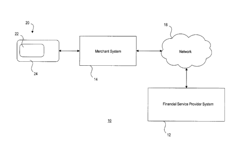
[038] Fig. 1 illustrates an exemplary transaction system 10.
Transaction
system 10 may include a computing system configured to receive and send
information
between the components of transaction system 10 and components outside of
transaction system 10. Transaction system 10 may include a financial service
provider
system 12 and a merchant system 14 communicating with each other through a
network
16. Transaction system 10 may include additional and/or alternative
components.
7
CA 2981875 2017-10-10
Attorney Docket No. 05793.3609-00000
[039] Financial service provider system 12 may include one or more computer
systems associated with an entity that provides financial services. For
example, the
entity may be a bank, credit union, credit card issuer, or other type of
financial service
entity that generates, provides, manages, and/or maintains financial service
accounts
for one or more customers. Financial service accounts may include, for
example, credit
card accounts, checking accounts, savings accounts, loan accounts, reward
accounts,
and other types of financial service accounts. Financial service accounts may
be
associated with physical financial service transaction cards, such as credit
or debit
cards that customers use to perform financial service transactions, such as
purchasing
goods and/or services online or at a point of sale (POS) terminal. Financial
service
accounts may also be associated with electronic financial products and
services, such
as a digital wallet or similar account that may be used to perform electronic
transactions, such as purchasing goods and/or services online.
[040] Merchant system 14 may include one or more computer systems
associated with a merchant. For example, merchant system 14 may be associated
with
an entity that provides goods and/or services (e.g., a retail store). The
merchant may
include brick-and-mortar location(s) that a customer may physically visit and
purchase
goods and services using the transaction cards. Such physical locations may
include
computing devices (e.g., merchant system 14) that perform financial service
transactions with customers (e.g., POS terminal(s), kiosks, etc.).
Additionally or
alternatively, merchant system 14 may be associated with a merchant who
provides an
electronic shopping environment, such as a website or other online platform
that
consumers may access using a computer through a browser, a mobile application,
or
8
CA 2981875 2017-10-10
Attorney Docket No. 05793.3609-00000
similar software. Merchant system 14 may include a client device, such as a
laptop
computer, desktop computer, smart phone, or tablet, which a customer may
operate to
access the electronic shopping mechanism.
[041] Network 16 may include any type of network configured to facilitate
communications and data exchange between components of transaction system 10,
such as, for example, financial service provider system 12 and merchant system
14.
Network 16 may include, but is not limited to, Local Area Networks (LANs) and
Wide
Area Networks (WANs), such as the Internet. Network 16 may be a single network
or a
combination of networks. Network 16 is not limited to the above examples and
transaction system 10 may implement any type of network that allows entities
(shown
and not shown) of transaction system 10 to exchange data and information.
[042] Transaction system 10 may be configured to conduct a transaction using
a transaction card 20. In some embodiments, financial service provider system
12 may
provide transaction card 20 to a customer for use in conducting transactions
associated
with a financial service account held by the customer. For example, the
customer may
use transaction card 20 at a merchant location to make a purchase. During the
course
of the purchase, information may be transferred from transaction card 20 to
merchant
system 14 (e.g., a point of sale device). Merchant system 14 may communicate
with
financial service provider system 12 via network 16 to verify the information
and to
complete or deny the transaction. For example, merchant system 14 may receive
account information from transaction card 20. Merchant system 14 may transmit
the
account information and a purchase amount, among other transaction
information, to
financial service provider system 12. Financial service provider system 12 may
settle
9
CA 2981875 2017-10-10
Attorney Docket No. 05793.3609-00000
the transaction by transferring funds from the customer's financial service
account to a
financial service account associated with the merchant.
[043] While transaction system 10 and transaction card 20 are depicted and
described in relation to transactions that involve customers, merchants, and
financial
service providers, it should be understood that these entities are used only
as an
example to illustrate one environment in which transaction card 20 may be
used.
Transaction card 20 is not limited to financial products and may be any
physical card
product that is configured to store and/or transmit information. For example,
transaction
card 20 may be an identification card configured to provide information to a
device in
order to identify the holder of the card (e.g., a driver's license).
[044] In some embodiments, transaction card 20 may further include a data
storage component 22 disposed on or in a transaction card frame ("frame") 24.
As used
herein, a "data storage component" may be one or more devices and/or elements
configured to receive, store, process, provide, transfer, send, delete, and/or
generate
information. For example, data storage component 22 may be a microchip (e.g.,
a
Europay, MasterCard, and Visa (EMV) chip), a communication device (e.g., Near
Field
Communication (NFC) antenna, Bluetooth device, WiFi device), a magnetic
strip, a
barcode, Quick Response (QR) code, etc. Data storage component 22 may be
secured
(or affixed, attached) to frame 24 in such a way that allows frame 24 to carry
data
storage component 22 while maintaining a utility of data storage component 22
(i.e.,
allowing data storage component 22 to interact with merchant system 14). Data
storage
component 22 may be configured to ensure that data storage component 22
functions
properly during data storage and transmission; for example, ensuring that a
card
CA 2981875 2017-10-10
, .
_
Attorney Docket No. 05793.3609-00000
containing an RFID (radio frequency identification) device shielded by a
material layer
can still be properly read by an RFID reader through the material layer.
[045] Figs. 2A and 2B are front and rear views, respectively, of an exemplary
transaction card 28 with a first data storage component 22A (e.g., a
microchip) and a
second data storage component 22B. Fig. 2A shows a front surface 30 of card 28
with a
length defined as Lc, and Fig. 2B shows a rear surface 32 of card 28, with
data storage
component 22B exposed (i.e., a magnetic strip in this exemplary embodiment).
The
magnetic strip may have a length Lm which may be equal to or less than the
card length
Lc, and may be flush with rear surface 32.
[046] In some embodiments, visual details, such as transaction information,
aesthetic designs, images, etc., may be visible from a first side 30 of card
28. For
example, a customer name, an account number, date information, bank
information,
transaction system information (e.g. Visa, MasterCard, etc.), a design or
logo, a
signature associated with the customer, and/or other information may be
visible from
first side 30. In some embodiments, visual information may also or
alternatively be
visible from second side 32 of card 28. Such visual details may be generated
during a
process of forming the card (e.g., pressing, laminating, injection molding,
etc.) or during
a process subsequent to card formation (e.g., milling, laser cutting, etching,
stamping,
etc.). In some embodiments, such visual details may be included on one or more
surfaces of transaction card 28 and visible from first and/or second side 30,
32.
[047] Fig. 3 illustrates card 28 with a section line 4-4 along its length.
Fig. 4A is
a magnified cross-sectional view of card 28 along line 4-4. As shown, card 28
may
include a housing component (or "housing") 34, an inlay component (or "inlay")
36, one
11
CA 2981875 2017-10-10
Attorney Docket No. 05793.3609-00000
or more light sources 40, and a power source 42 electronically connected to
the light
sources 40. Power source 42 may be configured to supply electrical power to
light
sources 40, which may be configured to emit light through inlay 36. Housing 34
and/or
inlay 36 may include a recess 44 configured to house and expose data storage
device
22A. As used herein, the term "inlay" may refer to material or a component set
into a
surface of another material or component.
[048] Housing 34 may be made of PVC, PC, or other similar materials, and
may be manufactured using a molding process, such as an injection-molding
process or
a compression-molding process. In other embodiments, housing 34 may be formed
of a
resin mixture comprising one or more of a thermoplastic elastomer (TPE),
polybutylene
terephthalate (PBT), an acetal homopolymer, and/or other materials. In some
embodiments, the TPE and/or other materials may be selected to provide card 28
with a
"soft-touch feel" (i.e., a haptic sensation that occurs when a person touches
something
that, for example, feels soft, smooth, and/or satiny). In some embodiments,
the resin
mixture may include a polyester elastomer, a block copolymer, a thermoplastic
olefin,
an elastomeric alloy, a thermoplastic polyurethane, a thermoplastic
copolyester, or a
thermoplastic polyamide. In some embodiments, housing 34 may be non-opaque
(e.g.,
translucent, transparent, clear, etc.). That is, housing 34 may be formed of a
material
that is non-opaque after manufacturing is complete (e.g., after setting).
[049] Inlay 36 may be a light-penetrable inlay. That is, inlay 36 may be
configured to allow light to pass therethrough (i.e., a device through which
visible light
may pass). In some embodiments, inlay 36 may be clear, transparent, or
translucent. In
some embodiments, light passing through inlay 36 may be diffused to achieve
desired
12
CA 2981875 2017-10-10
Attorney Docket No. 05793.3609-00000
aesthetic and/or operational requirements. That is, inlay 36 may have light-
diffusing
properties or be a light-diffusing layer. In some embodiments, inlay 36 may be
backlit by
light sources 40 to produce a desired aesthetic appearance of card 28 (e.g.,
to cause
card 28 to appear "lit up" and/or to cause visual details on card 28 to become
visible or
appear differently when backlit or edge lit).
[050] Light
diffusing properties of inlay 36 may function to spread light emitted
by light sources 40 across inlay 36 to create a more even distribution of
light intensity,
as seen by a card user through inlay 36. In this way, desired lighting
characteristics may
be achieved while reducing the appearance of localized higher-intensity light
(or "hot
spots") caused by light sources 40 (e.g., sources of direct light, such as
LEDs). The light
diffusing function of inlay 36 may also permit for edge-lighting of inlay 36
(discussed
further below), which may require fewer light sources 40 than backlighting
configurations, thereby reducing the cost of card 28 and improving its
operating
efficiency.
[051] As shown in Fig. 4A, housing 34 may include a first housing surface 46,
and a second housing surface 48 opposite the first housing surface 46. Inlay
36 may
include a first inlay surface 50, and a second inlay surface 52 opposite the
first inlay
surface 50. Light sources 40 may disposed on or in card housing 36 and
configured to
emit light through inlay 36 (i.e., when energized or powered by power source
42).
Housing 34 and inlay 36 may be joined via first housing surface 46 and second
inlay
surface 52 such that light emitted by light source(s) 40 passes through inlay
36. That is,
first housing surface 46 and second inlay surface 52 may be adjacent and/or in
contact
with one another when housing 34 and inlay 36 are joined. For example, housing
34
13
CA 2981875 2017-10-10
Attorney Docket No. 05793.3609-00000
and inlay 36 may be joined using an adhesive material, interconnecting
features (e.g.,
snap fit, tongue and groove, etc.), fasteners (e.g., screws, nuts, bolts,
rivets, etc.),
and/or other joining mechanisms or techniques.
[052]
Light source 40 may be an electronic, photoluminescent (i.e., "glow in the
dark"), or other type of device configured to emit light. For example, in some
embodiments, light source 40 may be a light emitting diode (LED). Suitable
LEDs may
be selected based on, among other factors, size limitations, color
requirements, and
power usage limitations. For instance, card 28 may have an overall thickness
of 0.030
inches (0.762 mm) (e.g., pursuant to ISO standards for transaction card
thickness), and
therefore a relatively small LED may be used as light source 40. For example,
LEDs
having a footprint of the standard size 0201 (0.002 x 0.001 x 0.001 inches)
may be
suitable for use in card 28. It is noted that other LEDs of different sizes
may be used,
depending on the dimensions of the LED and/or the dimensions of the card
components
(e.g., housing 34, inlay 36, etc.). It should be noted that light source 40
may be or
include other types of electronic light sources, such as light bulbs (e.g.,
incandescent,
fluorescent, halogen, etc.). Size and power constraints may dictate the types
of
electronic light sources that can be used with card 28 as light source 40.
[053] In other embodiments, photoluminescent materials may be used as light
source 40. For example, light source 40 may be or include a photoluminescent
coating,
such as a photoluminescent epoxy or paint. In other embodiments, a
photoluminescent
pigment or other photoluminescent material may be added to inlay 36 during its
formation. Suitable photoluminescent materials may be those that store light
photons
when exposed to an external light source (e.g., ambient light, direct
sunlight, another
14
CA 2981875 2017-10-10
Attorney Docket No. 05793.3609-00000
light source, etc.) and continue to emit light after exposure to the light
source has
ended.
[054] When multiple light sources 40 are used, one or more colors of light
sources 40 (i.e., light sources that emit different colors) may be
implemented,
depending on design and utility requirements. For example, in some
embodiments, light
sources 40 may be all the same color (e.g., red, orange, yellow, green, blue,
etc.). In
other embodiments, light sources 40 configured to emit different colors of
light may be
installed to generate desired patterns of colored light for aesthetic or
functional
purposes. For example, in some embodiments, LEDs of different colors may be
configured to indicate the voltage or state of charge (SOC) of power source
42. In an
exemplary embodiment, an LED of a first color (e.g., green) may be configured
to be
energized when power source 42 is above a first voltage or SOC. An LED of a
second
color (e.g., yellow) may be configured to be energized when power source 42 is
above a
second and below the first voltage or SOC. An LED of a third color (e.g., red)
may be
configured to be energized when power source 42 is below the second voltage or
SOC.
It is noted that other types of information may be indicated based on the
location, color,
flashing pattern, etc., of light sources 40.
[055] In some embodiments, as shown in Fig. 4A, inlay 36 may be comprised
of a single-layer. In other embodiments, inlay 36 may be formed of multiple
components
(e.g., multiple layers). For example, as shown in Fig. 4B, inlay 36 may
include a light-
penetrable layer 54 and a backer layer 56 (serving as structural backing
support for
layer 54). Light-penetrable layer 54 and backer layer 56 may be joined by a
suitable
joining or fastening mechanism that permits light to pass from second inlay
surface 52
CA 2981875 2017-10-10
Attorney Docket No. 05793.3609-00000
to first inlay surface 50. For example, Light-penetrable layer 54 and backer
layer 56 may
be joined by an adhesive layer (not shown), which may be, for example, 1 mil
or greater
in thickness (depending on the overall thickness of card 28 and the
thicknesses of light-
penetrable layer 54 and backer layer 56, and on the requirements of the
adhesive).
[056] In some embodiments, light-penetrable layer 54 may be or include a light
diffuser material, such as a light diffuser film. For example, light-
penetrable layer 54
may be a one- or two-sided diffuser film configured to distribute light evenly
across its
surface. Each respective side of the light diffuser material may be clear,
translucent, or
have a matte finish. In some embodiments, the light diffuser material may
comprise
multiple layers, such as guide layers, diffusion layers, prism layers, etc.
[057] In other embodiments, light-penetrable layer 54 may be clear,
transparent, translucent, tinted, polarized, textured, hazed, colored, or
otherwise
configured to affect (or not affect) light passing therethrough. In some
embodiments,
light-penetrable layer 54 may have a reflective backing. That is, light-
penetrable layer
54 may be adjacent a reflective material, such as a mirror, polished metal,
metal-coated
or metal-plated material, a coated or otherwise reflective glass or plastic
material, etc. A
reflective backing may reflect back light passing through light-penetrable
layer 54 to
enhance or brighten the appearance of card 28.
[058] The thickness of light-penetrable layer 54 may be selected based on
desired light-altering performance, the thickness of backer layer 56, and/or
structural
requirements of inlay 34. For example, light-penetrable layer may be from 3
mils (i.e.,
3/1000 of an inch) to 20 mils thick, depending on the thickness of backer
layer 56 and/or
16
CA 2981875 2017-10-10
. ,
Attorney Docket No. 05793.3609-00000
_
other components. Light-penetrable layer 54 may be, for example, from 3 to 20
mils,
from 3 to 15 mils, from 3 to 10 mils, from 3 to 5 mils, or less than 3 mils
thick.
[059] In some embodiments, light-penetrable layer 54 may be formed using a
lamination, injection molding, compression injection, sheet forming, or other
process. In
some embodiments, light diffusing materials, such as acrylic, polycarbonate
(PC),
polyethylene terephthalate (PET), and/or other materials may be used to form
light-
penetrable layer 54. In other embodiments, light-penetrable layer 54 may be or
include
one or more commercially available materials. For example, light-penetrable
layer 54
may be cut from a roll or sheet of light-penetrable commercially available
material.
Cutting, stamping, milling, laser cutting, and/or other processes may be used
to form
light-penetrable layer 54 from rolls or sheets of commercially available light-
penetrable
material.
[060] In some embodiments, light-penetrable layer 54 may be configured to
polarize light generated by light source 40 to alter the appearance of passing
light
and/or to provide a privacy function. For example, light-penetrable layer 54
may be
configured to restrict the angle at which visible light is emitted from inlay
36 (e.g., to
reduce visibility of details on card 28 from peripheral vantage points). To
achieve
polarizing functionality, light-penetrable layer 54 may, for example, include
polarizing
materials or a polarizing layer.
[061] Backer layer 56 may be a structural layer configured to support light-
penetrable layer 54 and facilitate the joining of inlay 36 to housing 34. In
some
embodiments, backer layer 56 may be formed of particular materials or be sized
to
improve the mechanical properties of card 28. For example, backer layer 56 may
be
17
CA 2981875 2017-10-10
Attorney Docket No. 05793.3609-00000
formed of stiffer, less flexible, and/or more dense materials than light-
penetrable layer
54. Backer layer 56 may be formed of, for example, injection molded plastic,
polycarbonate, acrylic, and/or other materials. The thickness of backer layer
56 may be
selected based on the overall thickness of card 28 (e.g., 30 mils) and may
range from
10-20 mils, depending on the thicknesses of housing 34 and light-penetrable
layer 54.
For example, backer layer 56 may be less than 20 mils, 10-2C) mils, 12-18
mils, 14-16
mils, 15 mils, or greater than 10 mils in thickness.
[062] With reference to Fig. 5, some embodiments of card 28 may be
configured such that light source(s) 40 is/are disposed between housing 34 and
inlay 36. For example, Fig. 5 shows a partially disassembled, magnified cross-
sectional
view of card 28, in which light sources 40 are disposed between first housing
surface 46
and inlay 36 (e.g., second inlay surface 52 of inlay 36). In embodiments
consistent with
the example of Fig. 5, backer layer 56 may be non-opaque (i.e., formed of non-
opaque
material) to permit light to travel through backer layer 56, and thus through
inlay 36.
[063] In
the configuration of the exemplary embodiment of Fig. 5, visual details
of card 28, such as transaction information (e.g., card number, customer name,
logos,
etc.), may be included on backer layer 56, which may be visible by the user
through
inlay 36 and/or made more visible (or appear differently) when light source(s)
40 is/are
emitting light. For example, a top surface 58 of backer layer 56 may be
etched, sanded,
laser-etched, carved, printed, milled, stamped, or otherwise processed to
include visual
details that are configured to be or become visible through inlay 36 when
light source(s)
40 is/are energized. In embodiments consistent with the example of Fig. 5,
light-
penetrable layer 56 may also or alternatively be processed to include visual
details.
18
CA 2981875 2017-10-10
Attorney Docket No. 05793.3609-00000
[064] With reference to Fig. 6, some embodiments of card 28 may be
configured such that light source(s) 40 is/are disposed between light-
penetrable layer
54 and backer layer 56. For example, Fig. 6 shows a partially disassembled,
magnified
cross-sectional view of card 28, in which light sources 40 are disposed
between top
surface 58 of backer layer 56 and a bottom surface 60 of light-penetrable
layer 54. In
embodiments consistent with the example of Fig. 6, backer layer 56 may be non-
opaque, opaque, and/or reflective (i.e., is formed of or includes reflective
material). For
example, top surface 58 of backer layer 56 may include a reflective coating or
be
covered with a layer of reflective material (e.g., metal, metallic coating,
reflective spray
or film, etc.) to reflect light through light-penetrable layer 54.
[065] In the configuration of the exemplary embodiment of Fig. 6, visual
details
of card 28, such as transaction information (e.g., card number, customer name,
logos,
etc.), may be included or formed on or in the top or bottom surface of light-
penetrable
layer 54 (i.e., on first inlay surface 50 or bottom surface 60 of light-
penetrable layer,
respectively). In this way, visual details of card 28 may be visible by the
user through
inlay 36 and/or made more visible (or appear differently) when light source(s)
40 is/are
energized (i.e., emitting light). Light-penetrable layer 54 may be etched,
sanded, laser-
etched, carved, printed, milled, stamped, or otherwise processed to include
visual
details that are configured to be or become visible through inlay 36 when
light source(s)
40 is/are energized.
[066] Fig. 7A illustrates card 28 with a section line 7B-7B along its
width.
Fig. 7B is a magnified, partially disassembled, isometric cross-sectional view
of card 28
along line 7B-7B. In embodiments consistent with the example of Fig. 7B,
housing 34
19
CA 2981875 2017-10-10
Attorney Docket No. 05793.3609-00000
may include a cavity 62 having a cavity wall 64. Inlay 36 may be configured to
fit into or
be positioned within cavity 62 such that a side portion 66 of inlay 36 (e.g.,
a side portion
of light-penetrable layer 54 and/or backer layer 56) is adjacent cavity wall
64. Light
source(s) 40 may also be positioned on or on or in (e.g., recessed into)
cavity wall 64. In
this way, light source(s) 40 may be configured to project (i.e., emit) light
laterally through
inlay 36. Laterally projected light from light source(s) 40 may be distributed
and/or
scattered throughout inlay 36 to achieve a more even light distribution across
front
surface 30 of card 28. In other words, light source(s) 40 may be configured to
edge-light
inlay 36. Edge-lighting may permit for fewer light sources 40 to be used,
thereby
reducing the cost and increasing the efficiency of card 28.
[067] In some embodiments, as shown in Figs. 8 and 9, card 28 may include a
switch 68 configured to activate and deactivate the light source(s) 40. With
reference to
Fig. 8, in some embodiments, switch 68 may be disposed between light-
penetrable
layer 54 and backer layer 56. For example, switch 68 may be disposed in a
recess 70
on top surface 58 of backer layer 56. In other embodiments, switch 68 may be
disposed
directly on top surface 56 of backer layer 56 (i.e., not within a recess).
Switch 68 may be
a pressure switch (i.e., a pressure-sensitive or pressure-activated switch)
configured to
activate light source(s) 40 when a user presses on card 28 (e.g., presses
inlay 36 and
housing 34 together). For instance, inlay 36 (i.e., light-penetrable layer 54
and/or backer
layer 56) may be configured to flex under pressure applied to card 28, thereby
exerting
a force on switch 68 sufficient to energize light source(s) 40. In other
embodiments,
switch 68 may be a touch sensor (e.g., a capacitive-type touch sensor)
positioned at or
CA 2981875 2017-10-10
-
Attorney Docket No. 05793.3609-00000
sufficiently near first inlay surface 50 to detect when a user touches switch
68 (i.e. to
activate light source(s) 40).
[068] In other embodiment, with reference to Fig. 9, switch 68 may be
disposed between housing 34 and inlay 36. For example, switch 38 may be
disposed
between first housing surface 46 and the bottom of inlay 36 (e.g., second
inlay surface
52). For example, switch 68 may be disposed in recess 70 on second inlay
surface 52.
In other embodiments, switch 68 may be disposed directly on second inlay
surface 52
(i.e., not within a recess).
[069] Fig. 10 shows a schematic illustration of an exemplary circuit 72
consistent with embodiments of the present disclosure. As shown, light source
40 may
be electrically connected to power source 42 (e.g., via wires, flat wires,
printed
conductors, a circuit board, etc.). Switch 68 may be electrically connected to
light
source 40 and power source 42, and may be configured to activate and
deactivate the
light source by connecting and disconnecting light source 40 from power source
42. It
should be understood that other circuit components may also be included, such
as
capacitors, resistors, memory, a processor, etc. Light source 40 may include a
plurality
of light sources (e.g., LEDs) connected in parallel to power source 42 (e.g.,
by a bus or
other conductive component). In other embodiments, one or more light sources
may be
connected in series.
[070] In some embodiments, power source 42 may be or include one or more
batteries. For example, power source 42 may include a lithium-ion battery or
other type
of non-rechargeable or single-use battery. Batteries used in power source 42
may be
thin and flexible. For example, commercially available flexible lithium
batteries less than
21
CA 2981875 2017-10-10
. ,
-
Attorney Docket No. 05793.3609-00000
2 mils thick may be used. Battery thickness may exceed 2 mils depending on the
thickness of card 28 and of its components (e.g., inlay 36 and housing 34).
The lifespan
of a non-rechargeable battery may be determined by type and quantity of light
sources
40 included in card 28.
[071] In another embodiment, with reference to Figs. 11A-11B, card 28 may
include a rechargeable power source 74. Fig. 11A illustrates card 28 with a
section line
11B-11B along its width. Fig. 11B is a magnified cross-sectional view of card
28 along
line 11B-11B. In embodiments consistent with the example of Fig. 11B,
rechargeable
power source 74 may be disposed on or in housing 34 and configured to supply
power
to the light source. Rechargeable power source 74 may be or include, for
example, a
lithium polymer battery or other type of rechargeable or multiple-use battery.
Batteries
used in rechargeable power source 74 may be thin and flexible. For example,
commercially available flexible lithium polymer batteries less than 2 mils
thick may be
used. Battery thickness may exceed 2 mils depending on the thickness of card
28 and
of its components (e.g., inlay 36 and housing 34). Rechargeable battery 74 may
include
charging electrodes 76 configured to conduct an electrical current from a
charging
device into rechargeable battery 74. Charging electrodes 76 may be configured
to be
exposed, for example, at front surface 30 of card 28. In other embodiments,
charging
electrodes 76 may be exposed at a rear surface 78 opposite front surface 30.
[072] Fig. 12 shows a schematic illustration of an exemplary charging
device 80 configured to receive card 28 for charging rechargeable battery 74.
In the
example of Fig. 12, charging device 80 may be configured to receive card 28
through an
open end 82. A charging terminal 84 may be disposed on or in charging device
80 and
22
CA 2981875 2017-10-10
. ,
= Attorney Docket No. 05793.3609-00000
include charging electrodes 86 configured to engage charging electrodes 76 of
card 28.
Charging device 80 may include a charging circuit 88 for conditioning
electrical current
from an external power source. It should be noted that card 28 and charging
device 80
may be configured to utilize other configurations or types of charging
systems, such as
inductive charging systems, solar power systems (e.g., solar panel or thin-
film solar
power systems), and/or other types of charging systems.
[073] In some embodiments, card 28 may include an internal power generator
to charge rechargeable battery 74. For example, card 28 may include a kinetic
generator, such as a micro-generator (e.g., a claw-pole generator, a lavet
generator, an
air coil generator, oscillating mass generator, piezoelectric material
generator, etc.). In
other embodiments, card 28 may include a thermoelectric generator, such as a
semiconductor-type thermoelectric generator configured to generate electricity
from a
temperature gradient. In such embodiments, a user may be able to place one
side of
card 28 on a hot or cool surface (relative to the other side of card 20) to
charge battery
74. In other embodiments, card 28 may include solar panels or thin-film solar
cells (e.g.,
photovoltaic materials) for harvesting solar energy. In some embodiments,
light-
penetrable layer 54 may comprise a transparent photovoltaic material
configured to
convert light energy into electricity while also allowing light to pass
therethrough.
[074] Fig. 13 is a flowchart showing an exemplary method/process 1300 for
forming a transaction card according to some embodiments of the present
disclosure. It
is noted that the steps associated with method 1300 may be performed in in
different
orders than the order in which they are numbered and/or described. Method 1300
may
include forming a card housing component having a first housing surface, and a
second
23
CA 2981875 2017-10-10
Attorney Docket No. 05793.3609-00000
=
housing surface opposite the first housing surface (Step 1310). For example
Step 1310
may include forming housing 34 from PVC, PC, or other similar materials, using
a
manufacturing process, such as a molding process (e.g., an injection-molding
process
or a compression-molding process). In other embodiments, housing 34 may be
formed
of a resin mixture comprising one or more of a thermoplastic elastomer (TPE),
polybutylene terephthalate (PBT), an acetal homopolymer, and/or other
materials. In
some embodiments, the TPE and/or other materials may be selected to provide
card 28
with a "soft-touch feel" (i.e., a haptic sensation that occurs when a person
touches
something that, for example, feels soft, smooth, and/or satiny). In some
embodiments,
method 1310 may include forming housing 34 from a resin mixture comprising a
polyester elastomer, a block copolymer, a thermoplastic olefin, an elastomeric
alloy, a
thermoplastic polyurethane, a thermoplastic copolyester, or a thermoplastic
polyamide.
In some embodiments, housing 34 may be non-opaque (e.g., translucent,
transparent,
clear, etc.). That is, housing 34 may be formed of a material that is or
becomes non-
opaque after manufacturing is complete (e.g., after setting)
[075] Method 1300 may further include forming light-penetrable inlay 34 with
first inlay surface 50 and second inlay surface 52 opposite first inlay
surface 50 (Step
1320). In some embodiments, inlay 34 may be formed as a unitary component, as
shown in Fig. 4A, for example, using a molding process, a stamping process, a
sheet
forming process, or another manufacturing process. In other embodiments, Step
1320
may include forming inlay 34 by forming and joining backer layer 56 and light-
penetrable
layer 54. Backer layer 56 and light-penetrable layer 54 may each be
respectively formed
using a molding process, a stamping process, a sheet forming process, or
another
24
CA 2981875 2017-10-10
= Attorney Docket No. 05793.3609-00000
manufacturing process. Step 1320 may also include joining backer layer 56 and
light-
penetrable layer 54, for example, using epoxy or a lamination process. In some
embodiments, a reflective coating may also be provided on backer layer 56
during step
1320 to allow light to be reflected through light-penetrable layer 54. In some
embodiments, step 1320 may further include providing visual details of card
28, such as
personal information, on light-penetrable layer 54 and/or backer layer 56,
such as by
etching, sanding, laser-etching, carving, printing, milling, stamping, etc.
[076] As used herein, the term "forming" with regard to steps of forming or
manufacturing components or subcomponents of card 28 may include providing
such
components or subcomponents (e.g., by providing commercially available or
commissioned components).
[077] Method 1300 may further include forming cavity 62 within housing 34
(Step 1330). Step 1330 may include forming cavity wall 64. In some
embodiments,
cavity 62 may be formed when housing 34 is formed (i.e., formed during the
forming
process of housing 34). In other embodiments, step 1330 may be a separate
process
that includes subsequently forming cavity 64 within housing 34, such as by
milling, laser
cutting, etc.
[078]
Method 1300 may further include providing light source 40 and disposing
it on or in card housing 34 (Step 1340). In some embodiments, step 1340 may
include
providing an electronic, photoluminescent (i.e., "glow in the dark"), or other
type of
device configured to emit light from housing 34 (e.g., from cavity 62). For
example, in
some embodiments, step 1340 may include providing one or more light emitting
diodes
(LED) or another type of electronic light source, such as an incandescent or
fluorescent
CA 2981875 2017-10-10
.
Attorney Docket No. 05793.3609-00000
source. In other embodiments, step 1340 may include providing a
photoluminescent
material, such as a photoluminescent coating (e.g. ,a photoluminescent epoxy
or paint)
on one or more of first housing surface 46, top surface 58 of backer layer 56,
or second
inlay surface 52. Alternatively, a photoluminescent pigment or other
photoluminescent
material may be added to inlay 36 during its formation. In some embodiments,
step
1340 may include providing multiple light sources 40, which may be configured
to emit
different colors of light.
[079] In some embodiments, with reference to Fig. 5, step
1340 may include
providing light source(s) 40 between inlay 36 and housing 34 (e.g., between
first
housing surface 46 and second inlay surface 52). In other embodiments, with
reference
to Fig. 6, step 1340 may include providing light source(s) between top surface
58 of
backer layer 56 and a bottom surface 60 of light-penetrable layer 54. In other
embodiments, step 1340 may include providing light source(s) 40 between inlay
36 and
housing 34 by disposing light source(s) 40 on (e.g., directly on or in a
recess on) cavity
wall 64, as shown in Fig. 7B.
[080] Method 1300 may further include providing a power source (e.g., non-
rechargeable power source 42 or rechargeable power source 74) and disposing
the
power source on or in housing 34 (step 1350). The method may further include
electronically connecting light source(s) 40 to the power source (Step 1360)
via a bus or
other conductor. In some embodiments, the method may further include
electronically
connecting switch 68 to light source 40 (Step 1370) (e.g., between light
source(s) 40
and the power source) for activating and deactivating light source 40.
26
CA 2981875 2017-10-10
.
Attorney Docket No. 05793.3609-00000
[081] Method 1300 may further include joining housing 34 and inlay 36 at first
housing surface 46 and the second inlay surface 52 such that light emitted by
light
source 40 passes through inlay 30 (Step 1380). As described above, and with
reference
to Figs. 4A-4B, housing 34 and inlay 36 may be joined with light source(s) 40
between
inlay 36 and housing 34, or with light source(s) 40 between light-penetrable
layer 54
and backer layer 56. In some embodiments, and with reference to Fig. 7B,
housing 34
and inlay 36 may then be joined with light sources 40 between inlay 36 and
cavity wall
64 of housing 34. Inlay 36 and housing 34 may be joined, for example, using an
epoxy
or other joining method, as described above.
[082] While illustrative embodiments have been described herein, the scope
includes any and all embodiments having equivalent elements, modifications,
omissions, combinations (e.g., of aspects across various embodiments),
adaptations or
alterations based on the present disclosure. For example, the order of the
steps of the
above exemplary method may be rearranged in any preferred or suitable order,
or any
step may be removed or added.
[083] The elements in the claims are to be interpreted broadly based on the
language employed in the claims and not limited to examples described in the
present
specification or during the prosecution of the application, which examples are
to be
construed as non-exclusive. It is intended, therefore, that the specification
and
examples be considered as example only, with a true scope and spirit being
indicated
by the following claims and their full scope of equivalents.
27
CA 2981875 2017-10-10