Note: Descriptions are shown in the official language in which they were submitted.
CA 02982473 2017-10-11
1
DESCRIPTION
MULTIPOLE CONNECTOR, CONNECTOR DEVICE, CASE, AND METHOD FOR
CONNECTING CABLE TO MULTIPOLE CONNECTOR
Field
[0001] The present invention relates to a multipole
connector, a connector device, a case, and a method for
connecting a cable to the multipole connector, and
particularly to a structure of the connection between a
cable and a connector.
Background
[0002] A conventional shielded cable connecting method
has been disclosed in which a plurality of coaxial cables
are connected to a multipole connector, such as a D-SUB (D-
subminiature) and a micro D-SUB, while maintaining noise
immunity. The D-SUB and the micro-D-SUB are some of the
widespread connector standards and are widely used mainly
for connecting computers and peripheral devices to each
other. The D-SUB and the micro D-SUB are configured to
have two to four rows of pin contacts or socket contacts
that are surrounded by a metal shield having a shape
resembling the letter "D".
[0003] Patent Literature 1 discloses an example of a
method of connecting, to a connection target circuit,
internal conductors and external conductors of a plurality
of coaxial cables connected to a connector. In Patent
Literature 1, a technology is disclosed in which the side
portion of a ground plate is pressed against one side of a
base insulator such that it is deformed, thereby bringing a
plurality of ground contacts into pressure-contact with the
ground plate.
CA 02982473 2017-10-11
r
r
2
[0004] Moreover, in Patent Literature 2, there is a
disclosure of a technology for connecting shielded wires to
a multipole connector. The structure disclosed in Patent
Literature 2 is configured such that wires are first
crimped to the contacts of the connector and then the
connector is inserted into a connector housing.
[0005] Furthermore, Non Patent Literature 1 discloses a
cable-end shield connecting technology. In Non Patent
Literature 1, the ends of the cables are stripped of their
outer jackets and the grounding wire is connected to the
exposed shielding braids by soldering.
Citation List
Patent Literature
[0006] Patent Literature 1: Japanese Patent No. 3333936
Patent Literature 2: Japanese Patent No. 3111655
Non Patent Literature
[0007] Non Patent Literature 1: JERG-0-041A Electric
Wiring Process Standards for Space Applications
Summary
Technical Problem
[0008] However, with the structure in Patent Literature
1, the ground plate is interposed and held between the
ground contacts and the insulator; therefore, a slight
misalignment may cause poor contact. Moreover, this
structure cannot provide sufficient shielding properties
and has low noise immunity.
[0009] The structure in Patent Literature 2 is
configured such that wires are crimped to the contacts and
then the contacts are inserted into the connector housing,
but this structure inhibits size reduction. Moreover,
because the contacts of the multipole connector are of a
CA 02982473 2017-10-11
,
=
3
particular shape, the contacts need to be highly accurately
molded.
[0010] Furthermore, with the structure in Non Patent
Literature 1, it is necessary to solder the external
conductors one by one; therefore, this structure reduces
the ease of manufacturing and inhibits size reduction.
Moreover, this structure cannot provide sufficient
shielding properties and has low noise immunity.
[0011] As described above, with the above conventional
technologies, not only are shielding properties
insufficient but it is difficult to reduce the size of the
connection portion.
[0012] The present invention has been achieved in view
of the above and an object of the present invention is to
provide a multipole connector that is compact and has a
simple structure.
Solution to Problem
[0013] In order to solve the above problems and achieve
the object, an aspect of the present invention is a
multipole connector including a connector body that
includes a first end surface and a second end surface; a
plurality of contacts that are arranged and led to the
first end surface of the connector body; and a ground plate.
The multipole connector is connected to a cable in which
external conductors that are to be grounds and core wires
that are to be signal lines are insulated from each other
by an inner jacket and the outer side is sheathed with an
outer jacket. The signal lines are connected to the
contacts, respectively, the shield wires are connected
together on the ground plate, and the ground plate is
connected to at least one of the contacts.
CA 02982473 21317-113-11
4
Advantageous Effects of Invention
[0014] According to the present invention, an effect is
obtained where it is possible to obtain a multipole
connector that can have a simple structure and can be
reduced in size.
Brief Description of Drawings
[0015] FIG. 1 is a perspective view illustrating a
connector device according to a first embodiment.
FIG. 2 is a top view illustrating the connector device
according to the first embodiment.
FIG. 3 is a side view with partial cutaway of the
connector device according to the first embodiment.
FIG. 4 is a cross-sectional view of a coaxial cable
that is used in the connector device according to the first
embodiment, and is a cross-sectional view taken along line
A-A in FIG. 2.
FIG. 5 is a cross-sectional view of the coaxial cable
that is used in the connector device according to the first
embodiment, and is a cross-sectional view taken along line
B-B in FIG. 3.
FIG. 6 is an exploded perspective view of the
connector device according to the first embodiment.
FIG. 7 is a perspective view of a multipole connector
of the connector device according to the first embodiment.
FIG. 8 is a perspective view illustrating an
assembling process of the connector device according to the
first embodiment, where (a) is a perspective view with
partial cutaway of the whole connector device and (b) is an
enlarged perspective view of a relevant portion in (a).
FIG. 9 is a perspective view illustrating an
assembling process of the connector device according to the
first embodiment.
CA 02982473 2017-10-11
1 ,
,
FIG. 10 is a perspective view illustrating an
assembling process of the connector device according to the
first embodiment.
FIG. 11 is a perspective view illustrating a connector
5 device according to a second embodiment.
FIG. 12 is a top view illustrating the connector
device according to the second embodiment.
FIG. 13 is a side view with partial cutaway of the
connector device according to the second embodiment and is
a diagram illustrating a portion taken along line C-C in
FIG. 11.
FIG. 14 is a top view illustrating a modification of
the connector device according to the second embodiment.
FIG. 15 is a side view with partial cutaway of the
connector device according to the second embodiment.
FIG. 16 is a cross-sectional view illustrating a
shielded twisted cable that is used in a connector device
according to a third embodiment.
FIG. 17 is an explanatory diagram of the inside of a
connector device according to the third embodiment.
FIG. 18 is an explanatory diagram of the inside of a
connector device according to a fourth embodiment.
FIG. 19 is an explanatory diagram of a ground plate of
the connector device according to the fourth embodiment.
FIG. 20 is an explanatory cross-sectional view
illustrating a modification of the connector device
according to the fourth embodiment.
FIG. 21 is an explanatory diagram of the inside of a
connector device according to a fifth embodiment.
FIG. 22 is an explanatory cross-sectional view of the
connector device according to the fifth embodiment and
corresponds to a cross section taken along line E-E in FIG.
21.
CA 02982473 2017-10-11
6
FIG. 23 is an explanatory cross-sectional view of the
connector device according to the fifth embodiment and
corresponds to a cross section taken along line F-F in FIG.
21.
FIG. 24 is an explanatory diagram of the inside of a
connector device according to a sixth embodiment.
FIG. 25 is an explanatory cross-sectional view of the
connector device according to the sixth embodiment and
corresponds to a cross section taken along line G-G in FIG.
24.
Description of Embodiments
[0016] A multipole connector, a case that forms a back
shell, a connector device, and a method for connecting a
cable to the multipole connector according to embodiments
of the present invention will be described below in detail
with reference to the drawings. This invention is not
limited to these embodiments.
[0017] First Embodiment.
FIG. 1 is a perspective view illustrating a connector
device according to a first embodiment of the present
invention. FIG. 2 is a top view illustrating the connector
device according to the first embodiment; FIG. 3 is a side
view with partial cutaway of the connector device according
to the first embodiment; and FIG. 4 and FIG. 5 are cross-
sectional views of a coaxial cable and are respectively
cross-sectional views taken along line A-A in FIG. 2 and
line B-B in FIG. 3. A connector device 100 in the first
embodiment includes a connector body 10, which has a first
end surface 10T1 and a second end surface 10T2, which face
in opposite directions from each other; a plurality of
cables 20 connected to the connector body 10; and a case 30,
which has a back shell structure and houses a connection
CA 02982473 2017-10-11
.= ,
7
region where the connector body 10 and the cables 20 are
connected to each other. In the connector device in the
first embodiment, the external conductors of the coaxial
cables 20 that are to be grounds are first connected
together by soldering them to a ground plate 12 so as to
connect them to ground contacts 13G extending from the
second end surface 10T2 of the connector body 10, and the
core wires that are to be signal lines are connected to
signal line contacts 13S, thereby enabling the aligned
cables 20 to be drawn out, as the ground contacts 13G and
the signal line contacts 13S, to the first end surface 10T1
of the connector body 10. The solder-connected portions
are housed in the metal case having a shielding function.
Consequently, a compact connector device having a back
shell structure is obtained that has both a shielding
function for ensuring noise immunity and a back shell
function for ensuring mechanical strength as well as having
an excellent EMC performance.
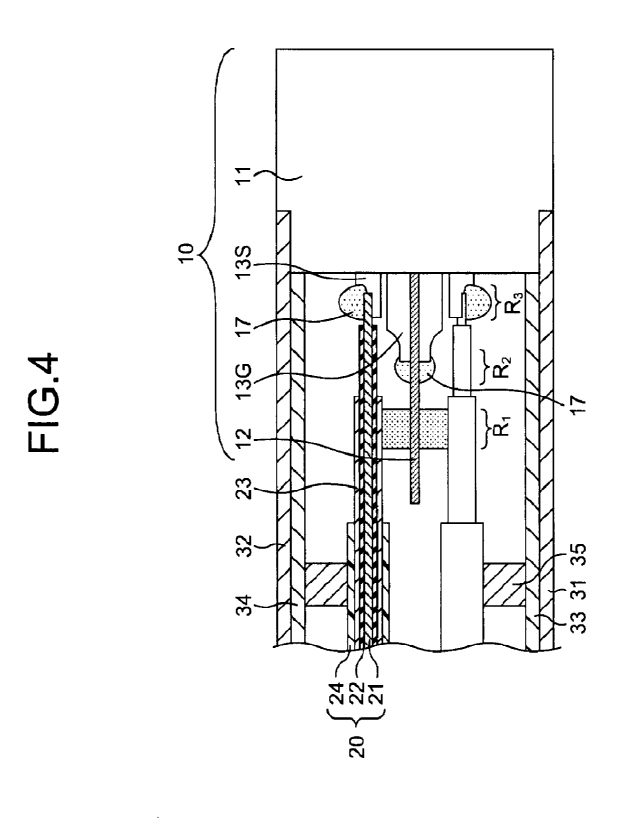
[0018] As illustrated in FIG. 3, a multipole connector
DS1 includes the connector body 10, the ground plate 12
made from a copper plate, and a plurality of contacts 13.
As illustrated in the overall view in FIG. 1, the connector
device includes the cables 20, the case 30, and the
multipole connector, which includes the connector body 10
and the ground plate 12. As illustrated in the enlarged
cross-sectional view of a relevant portion of the
connection portion of the cable 20 and the connector body
10 in FIG. 4, the connector body 10 includes a base 11,
which is a molded resin body covered with a metal plate;
and the contacts 13 extending from the base 11. The
contacts 13 are embedded in the molded resin body of the
base 11 and are provided in four rows. The other ends of
the contacts 13 form external contacts 16. The contacts 13
CA 02982473 2017-10-11
8
include the signal line contacts 13S, which are to be
connected to signal lines, and the ground contacts 13G,
which are to be connected to the grounds. The external
contacts 16 are connected to a contact of a receptacle or a
plug that is a connection partner (not illustrated).
Although the external contacts 16 are not illustrated in
FIG. 4, the external contacts 16 extend to the first end
surface 10T1 side of the connector body 10 and are used as
external connection terminals, as illustrated in FIG. 3.
During the assembling process illustrated in FIG. 6, the
ground plate 12 is held and secured within the case 30 but
is not directly secured to the case 30. The connector body
10 has a pair of mounting holes 14 on both sides of the
base 11. The connector device can, for example, be
attached and secured to the wall by inserting screws into
the mounting holes 14. The first end surface 10T1 side of
the connector body 10 forms a terminal tube 15, in which
the external contacts 16 are formed.
[0019] As illustrated in FIG. 1, the cables 20 are
arranged in two rows. FIG. 4 is an enlarged cross-
sectional view that includes the connection portion of one
of the cables 20 and the connector body 10, and FIG. 5 is
an enlarged cross-sectional view of the cable 20. As
illustrated in FIG. 4 and FIG. 5, the cable 20 is a coaxial
cable, in which a core wire 21, which functions as a signal
line, is sheathed with an inner jacket 22, which is in turn
sheathed with a ground mesh 23 made of a metal mesh, with
the ground mesh 23 being in turn sheathed with an outer
jacket 24. The ground mesh 23 is made by weaving copper
wires into a mesh and is known as a braided wire.
Alternatively, the ground mesh 23 with its surface coated
with solder may be used.
[0020] In the connection portion of the connector body
CA 02982473 2017-10-11
'
9
and the cable 20, the cable 20 is stripped of its outer
jacket 24 in order to make an electrical connection. First,
in a first region R1, in which the cable 20 is to be
connected to the ground plate 12, the outer jacket 24 is
5 stripped and thus the ground mesh 23 is exposed. The cable
is connected to the ground plate 12 by a solder layer 17
in the first region R. With this connection, because the
ground mesh 23 of the cable 20 is connected to the ground
plate 12 by the solder layer 17, the potentials of the
10 cable 20 and the ground plate 12 become equal. Then, on a
portion of the ground plate 12 corresponding to a second
region R2, the ground contact 13G in the contact 13 is
connected to the ground plate 12 by the solder layer 17 at
a position at which the ground contact 13G faces the ground
15 mesh 23 of the cable 20, and thus the ground mesh 23 and
the ground contact 13G are electrically connected via the
ground plate 12. The ground contacts 13G form the external
contacts 16, which are external connection terminals in the
second and third rows, as illustrated in FIG. 3. Further,
20 a third region R3 is formed, which is closer to the
connector body 10 than the second region R2 and in which
the inner jacket 22 is stripped and thus the core wire 21'
is exposed. In the third region R3, the signal line
contact 13S of the connector body 10 and the core wire 21
are connected by the solder layer 17. The signal line
contact 13S includes a dished recess at the tip thereof and
the core wire 21 is placed in the recess and is secured by
the solder layer 17.
[0021] As illustrated in the exploded perspective view
of the connector device in FIG. 6, the case 30 includes a
case body 31 formed from a plate-like body made of
stainless steel; and a case lid 32, which fits the case
body 31. The case body 31 includes a bottom plate 31b and
CA 02982473 21317-113-11
,
two side plates 31S erected on both sides of the bottom
plate 31b. The case lid 32 includes a lid plate 32F and
two lid side plates 32S erected on both sides of the lid
plate 32F. In a state where the connection portions of the
5 connector body 10 and the cables 20 are housed in the case
body 31, the two lid side plates 32S of the lid plate 32F
are fitted externally to the two side plates 31S of the
case body 31. These connection portions are secured to the
case 30 via an electromagnetic interference prevention
10 member 33, which is secured to part of the case body 31 and
is made of, for example, an elastic conductive mesh, and an
electromagnetic interference prevention member 34, which
covers the case lid 32 side of the connection portions.
Moreover, an electromagnetic interference prevention member
35 is provided on the outer side of the first region Ri,
the second region R2, and the third region R3, which are
the connection portions that are on the second end surface
10T2 side of the connector body 10. The electromagnetic
interference prevention member 35 allows the cables 20 to
pass therethrough but seals the gap between the cables 20
and the case 30. The ground plate 12 is not secured to the
case body 31 but is secured in place by inserting screws 36,
which are long enough to pass through the case body 31 and
the case lid 32, into mounting holes 32h provided at both
ends of the case body 31 and the case lid 32.
[0022]
Next, a description will be given of a method for
manufacturing the connector device 100, which includes a
method for connecting the cables 20 to the connector body
10 that forms the multiple connector. FIG. 7 to FIG. 10
are diagrams illustrating a method for manufacturing the
connector device 100. This method includes a process of
forming the connection portions by first stripping the
outer jackets 24 and the inner jackets 22 of the cables 20,
CA 02982473 2017-10-11
, o
11
by positioning the cables 20 such that the first region R1,
in which the ground meshes 23, which are external
conductors to be grounds, are exposed, is located over the
ground plate 12, the second region R2, which corresponds to
the tips of the ground contacts 13G of the contacts 13,
faces the first region Rl on the ground plate 12, and the
third region R3, which correspond to the tips of the signal
line contacts 13S of the contacts 13, is in contact with
the core wires 21, which are signal lines, and by soldering
the cables 20 to the multiple connector at the same time;
and a process of securing the cables 20 such that the
connection portions are covered with the case body 31, the
case lid 32, and the electromagnetic interference
prevention members 33, 34, and 35, which are arranged
inside the case body 31 and the case lid 32.
[0023] First, as illustrated in FIG. 7, to configure the
multipole connector, the connector body 10 is prepared,
which includes the base 11, which is a molded resin body
coated with metal; the ground plate 12 made from a copper
plate; and the contacts 13 extending from the base 11.
Although FIG. 7 illustrates only two rows of contacts 13,
i.e., the signal line contacts 13S and the ground contacts
13G, in reality, two rows of contacts are arranged in a
similar manner under the two of contacts illustrated in FIG.
7, i.e., the contacts 13 are actually arranged in four rows.
The connector body 10 is obtained by injecting resin into a
mold in which a lead frame including the contacts 13 and
the external contacts 16, such as contact pins, is placed.
The contacts 13 are embedded in the base 11 and are
provided in four rows. The other ends of the contacts 13
form the external contacts 16. Although the external
contacts 16 are not illustrated in FIG. 7, the external
contacts 16 extend to the first end surface 10T1 side of
CA 02982473 2017-10-11
12
the connector body 10 and are used as external connection
terminals, as illustrated in FIG. 3. The ground contacts
13G connected to the contact pins of the grounds are in
contact with the ground plate 12 and are connected thereto
by the solder layers 17.
[0024] Next, as illustrated in FIG. 8(a) and FIG. 8(b),
the ground contacts 13G are connected to the ground plate
12 and the ground meshes 23 are connected to the ground
plate 12. Then, the signal line contacts 13S are connected
to the core wires 21. At this point in time, as
illustrated in FIG. 8(a), the cables 20 with the outer
jackets 24 and the inner jackets 22 stripped are arranged
and soldered to the ground plate 12 and the contacts 13 of
the connector body 10 such that the connection portions
match in each of the first region Ri, the second region R2,
and the third region R3. FIG. 8(a) is a perspective view
with partial cutaway of the whole connector device and FIG.
8(b) is an enlarged perspective view of a relevant portion
in FIG. 8(a). Details are described with reference to FIG.
4 and FIG. 8(b). First, in the first region Ri, in which
the cables 20 are to be connected to the ground plate 12,
the outer jackets 24 are stripped and thus the ground
meshes 23 are exposed, and the ground meshes 23 are
connected to the ground plate 12 by the solder layer 17.
With this connection, the ground meshes 23 of the cables 20
on the lower layer side are also connected to the ground
plate 12. Then, on a portion of the ground plate 12
corresponding to the second region R2, the ground contacts
13G in the contacts 13 are connected to the ground plate 12
by the solder layers 17 at positions at which the ground
contacts 13G face the ground meshes 23 of the cables 20,
and thus the ground meshes 23 and the ground contacts 13G
are electrically connected via the ground plate 12.
CA 02982473 2017-10-11
13
Moreover, in the third region R3, which is closer to the
connector body 10 than the second region R2 and in which
the inner jackets 22 are stripped and thus the core wires
21 are exposed, the signal line contacts 13S are connected
to the core wires 21, which are signal lines, by the solder
layers 17. The connections in these three regions may be
made at the same time by heating a member that has been
plated with solder or may be made by heating each
connection portion while feeding solder to each connection
portion. In such a manner, the connections are made in the
first region Ri, the second region R2, and the third region
R3 by using the solder layers 17.
[0025] Thereafter, as illustrated in FIG. 9, the
connector body 10 to which the cables 20 are connected is
attached to the case body 31 such that the ground plate 12
is placed on the case body 31 with the electromagnetic
interference prevention member 33 therebetween.
[0026] Then, as illustrated in FIG. 10, the case lid 32
is fitted and attached to the case body 31 so that the
cables 20 that pass through the electromagnetic
interference prevention member 35 are constrained, thereby
securing the cables 20 in the case 30. As is apparent from
the exploded perspective view in FIG. 6, the connection
with the case 30 is made by interposing, between the case
body 31 and the case lid 32, the structure in which the
cables 20 and the connector body 10 are connected, and then
tightening the screws 36 that have passed through mounting
holes 12h provided at both ends of the ground plate 12 and
the mounting holes 32h of the case body 31 and the case lid
32.
[0027] In the connector device 100 configured in such a
manner, the ground meshes 23 of the cables 20 are soldered
to the ground plate 12, which is integrated with the ground
CA 02982473 2017-10-11
14
pins of a micro D-SUB; therefore, the connector device 100
is simple in structure and is easy to manufacture.
Moreover, the cables 20 can be connected in the connection
region that includes the first region Ri, the second region
R2, and the third region R3 without compromising the
structure of the coaxial cables. In other words, the
connection can be made while maintaining a constant
distance between the signal lines that are core wires and
the grounds that are external conductors. Consequently,
transmission characteristics that have no distortion can be
obtained.
[0028] Moreover, the length of the connection region
described above can be reduced to approximately one tenth
of that in the case when the connection is made by using
the connection method described in Non Patent Literature 1.
Thus, the connector device can be reduced in size. Because
the connection portions of the connector body 10 and the
cables 20 are housed in the case, the connection can be
made at low cost and with high EMC performance.
[0029] For example, the structure disclosed in Patent
Literature 1 has a communication performance of
approximately several tens of bits per second (Mbps),
whereas the connector device in the first embodiment can
have a communication performance of approximately a few
gigabits per second (Gbps).
[0030] Moreover, during the attaching process, cables
are easily connected by soldering by collectively
performing a thermal treatment after positioning; therefore,
the attaching process is extremely easy.
[0031] As described above, the connector device
according to the present embodiment has the following
characteristics.
(1) The wiring connection portions of the connector body 10
CA 029473 2017--11
and the cables 20 are covered with the case 30 made of a
conductor, such as a metal case, so as to implement both a
function as a shield case and a back shell function for
ensuring mechanical strength.
5 (2) With the case 30 described above, no external load is
applied to the soldered portions.
(3) As the structure in which a metal plate is soldered to
the micro D-SUB contacts in the second and third rows that
are assigned as the grounds among the four rows of the
10 micro D-SUB contacts, a common ground plate 12 is provided.
(4) The ground plate 12 described above is fastened, with
the screws 36, to the case 30, which includes the metal
case body 31 and the metal case lid 32, and thus has a
structure that ensures electrical continuity also with the
15 case 30.
(5) The ground meshes 23, which are external conductors of
the cables 20 that are coaxial cables, are soldered to the
ground plate 12 described above. Moreover, the core wires
21 are soldered to the signal line contacts 13S in the
first and fourth rows of the micro D-SUB. Consequently, it
is possible to keep the coupling state of the signal lines,
which are the coaxial core wires 21, and the grounds, which
include the ground meshes 23, as far as the connection
portion of the external contacts 16 and an external device;
therefore, noise immunity can be ensured.
(6) The second end surface 10T2 side of the cables 20 that
are coaxial cables is sealed by the electromagnetic
interference prevention member 35 provided in the case 30,
and the outer side of the electromagnetic interference
prevention member 35 is held by bringing the outer
conductor composed of the electromagnetic interference
prevention members 33 and 34 into contact with the case 30.
This improves the shielding function.
CA 02982473 2017-10-11
16
[0032] In the first embodiment, coaxial cables are used
as the cables 20; however, the first embodiment can also be
applied to multicore cables, such as pair cables and
twisted-pair cables, in addition to coaxial cables. The
multipole connector is not limited to a micro D-SUB and it
is obvious that the first embodiment can also be applied to
a D-SUB or other multipole connectors.
[0033] Moreover, the case body 31 is made of a stainless
steel plate; however, other materials, such as metal or
resin subjected to a process to make it function as an
electrical conductor, can also be used.
[0034] Furthermore, in the first embodiment, during the
assembling process illustrated in FIG. 6, the ground plate
12 is held and secured within the case 30 but is not
directly secured to the case 30; however, the ground plate
12 may be secured to the case 30. The shape of the ground
plate 12 can also be changed as appropriate.
[0035] Moreover, although the electromagnetic
interference prevention members 33, 34, and 35 are
effective at improving the EMC performance, it is not
necessary to always provide all the electromagnetic
interference prevention members 33, 34, and 35. If it is
not necessary to have an electromagnetic interference
prevention function at a position where an electromagnetic
interference prevention member is provided, the
electromagnetic interference prevention member may be
omitted. Furthermore, it is more effective if the
electromagnetic interference prevention member 33, 34, and
are arranged at positions as close as possible to the
30 connection region in which the cables 20 and the contacts
13 of the connector body 10 are connected to each other.
[0036] Second Embodiment.
FIG. 11 is a perspective view illustrating a connector
CA 02982473 2017-10-11
4
17
device according to a second embodiment of the present
invention. FIG. 12 is a top view illustrating the
connector device according to the second embodiment; and
FIG. 13 is a side view with partial cutaway of the
connector device according to the second embodiment and is
a diagram illustrating a portion taken along line C-C in
FIG. 11.
[0037] A connector device 100S in the second embodiment
is different from the first embodiment in that the case
body 31 and the case lid 32 are each made of an elastic
leaf spring and they are each provided with two lanced
pieces 38, which are cut and raised inward from notches 37
formed in a corresponding one of the case body 31 and the
case lid 32. The lanced pieces 38 press against the cables
20 from first and second main surfaces 30A and 30B of the
case 30, which face in opposite directions from each other,
so as to secure the cables 20. The lanced pieces 38 are
rolled inward as illustrated in FIG. 12, thereby having a
structure that can have improved shielding properties.
[0038] Other portions are similar to those in the
connector device 100 in the first embodiment; therefore,
the same components are denoted by the same reference
numerals. In a similar manner to the first embodiment, the
connector device 100S in the second embodiment includes the
connector body 10, which has the first and second end
surfaces 10T1 and 10T2, which face in opposite directions
from each other; the cables 20 connected to the connector
body 10; and the case 30, which has a back shell structure
and houses the connection region where the connector body
10 and the cables 20 are connected. In a similar manner to
the first embodiment, the cables 20 may be secured at the
end surface of the case 30 by a lanced piece (not
illustrated) and be shielded.
CA 02982473 2017-10-11
18
[0039] With the configuration described above, in
addition to the configuration of the connector device 100
in the first embodiment, the connector device 100S in the
second embodiment includes, in each of the case body 31 and
the case lid 32, the two lanced pieces 38, which are cut
and raised inward from the notches 37 formed in each of the
case body 31 and the case lid 32. The lanced pieces 38
press against the cables 20 from the first and second main
surfaces 30A and 30B of the case 30, which face in opposite
directions from each other, so as to secure the cables 20.
The lanced pieces 38 are rolled inward as illustrated in
FIG. 13. Consequently, the connector device 100S has a
structure that prevents noise from reaching the connection
region and thus improves the shielding properties.
Therefore, with the configuration described above, in
addition to the effect of the connector device 100 in the
first embodiment, the connector device 100S in the second
embodiment can obtain an effect where the EMC performance
can be improved without using any electromagnetic
interference prevention member and without increasing the
number of components.
[0040] In a similar manner to the connector device 100
in the first embodiment, the electromagnetic interference
prevention member 33, 34, and 35 can also be used in
combination, which results in the EMC performance being
improved.
[0041] FIG. 14 is a top view illustrating a connector
device 100P, which is a modification of the connector
device in the second embodiment. As illustrated in the
side view with partial cutaway of the connector device 100P
in FIG. 15, a cable lead-out portion may be sealed in such
a manner that electromagnetic interference prevention
members 35S are sandwiched between the lanced pieces 38.
CA 02982473 2017-10-11
. p op .
19
[0042] With the above configuration, the connector
device 100P in the modification can have improved EMC
performance compared to the connector device 100S in the
second embodiment.
[0043] In the connector device 100S in the second
embodiment and the connector device 100P in the
modification, the lanced pieces 38 are rolled on the outer
side of the electrical connection region where the
connector body 10 and the cables 20 are electrically
connected, and the lanced pieces 38, which are cut and
raised from the case body and the lid, press against the
cables 20 from both sides of the case 30. With the above
configuration, in addition to the effect of the connector
device 100 in the first embodiment, the EMC performance is
further improved. In the connector device 100P in the
modification, the lanced pieces 38 press against the cables
and moreover, the solder layers 17 are poured between
the lanced pieces 38 and the cables 20; therefore, an
improved sealing structure is obtained in addition to a
20 reliable connection. Moreover, because the electrical
connection region is sealed by a conductive member, the
magnetic shielding properties are further improved and thus
the EMC performance becomes extremely high.
[0044] Furthermore, the case body 31 and the case lid 32
are made of elastic bodies, and they have a structure that
can have improved shielding properties on the opening side
of the case due to the lanced pieces (not illustrated).
[0045] Third Embodiment.
Next, a connector device according to a third
embodiment will be described. A description has been given
in the first embodiment of a case where the cables 20 are
coaxial cables. In the third embodiment, a description
will be given of a case where cables 20T are shielded
CA 02982473 2017-10-11
twisted cables. FIG. 16 is a cross-sectional view
illustrating a shielded twisted cable, and FIG. 17 is a
diagram illustrating connection portions of the connector
body 10 and the cables 20T. FIG. 16 is a diagram
5 corresponding to the cross section taken along line D-D in
FIG. 17.
[0046] A connector device 100T in the third embodiment
is different from the first embodiment in the following two
points. That is, as illustrated in the enlarged cross-
10 sectional view in FIG. 16, the cable 20T is a twisted pair
cable having what is called a twisted pair structure in
which two core wires 21a and 21b are sheathed with inner
jackets 22a and 22b, respectively, and the inner jackets
22a and 22b are in turn sheathed with the ground mesh 23,
15 with the outermost layer being in turn sheathed with the
outer jacket 24. Moreover, the structure of the connection
between the ground plate 12 and the ground contacts 13G is
different due to a twisted pair cable being used.
[0047] As illustrated in FIG. 17, in the connector
20 device 100T in the third embodiment, ground contact pins
13GP, which are ground contacts of the connector body 10,
are placed on the ground plate 12; the ground plate 12 is
interposed between the ground contact pins 13GP and the
ground meshes 23 of the twisted pair cables 20T; and the
ground contact pins 13GP are connected to the ground meshes
23 by the solder layers 17. The core wires 21a and 21b are
connected to the signal line contacts 13S. The thin ground
contact pins 13GP are connected to the ground plate 12 by
the solder layers 17.
[0048] Other portions are similar to those in the
connector device 100 in the first embodiment; therefore,
the same components are denoted by the same reference
numerals. In a similar manner to the first embodiment, the
CA 02982473 2017-10-11
, 4 1
21
connector device 100T in the third embodiment includes the
connector body 10, which has the first and second end
surfaces 10T1 and 10T2, which face in opposite directions
from each other; the cables 20T connected to the connector
body 10; and the case 30, which has a back shell structure
and houses the connection region where the connector body
and the cables 20T are connected.
[0049] In the connector device 100T in the third
embodiment, with the above configuration, even when the
10 cables 20T, which are twisted pair cables, are connected to
the connector body 10, the cables 20T can still be mounted
with a compact structure. Moreover, the cables 20T can be
connected to the connector body 10 without significantly
changing the distance between the grounds and the core
wires of the cables 20T, which are twisted pair cables.
Furthermore, in addition to the effect of the connector
device 100 in the first embodiment, because the ground
contact pins 13GP of the connector body 10 and the ground
meshes 23 of the twisted pair cables are connected with
excellent electrical connectivity by interposing the ground
plate 12 therebetween, the ground contact pins 13GP, the
ground meshes 23, and the ground plate 12 can more reliably
be brought into contact with and pressed against each other
and the solder layers 17 are poured between the ground
contact pins 13GP, the ground meshes 23, and the ground
plate 12. Consequently, it is possible to obtain an
excellent sealing structure in addition to a reliable
connection. Because the cables 20T are sealed by a
conductive member, the magnetic shielding properties are
high and the magnetic interference prevention effect is
high.
[0050] The following configuration is also effective.
In this configuration, the ground plate 12 is made of a
CA 02982473 2017-10-11
22
thin conductive body having flexibility, such as metal foil,
and the ground plate 12 is interposed between the ground
contact pins 13GP and the ground meshes 23, which are
shielded wires of the cables 20T, thereby sealing the
second end surface 10T2 side of the base 11.
[0051] Moreover, the following configuration is also
effective. In this configuration, the ground plate 12 is
made of a conductive elastic body and the ground plate 12
is interposed between the ground contact pins 13GP and the
ground meshes 23, which are external conductors that are to
be the grounds, and the ground plate 12 is elastically
deformed so as to have irregularities, thereby sealing the
second end surface 10T2 side of the base 11.
[0052] The connector device 100T in the third embodiment
can inhibit interference with the signal line contacts 13S
by using the ground contact pins 13GP extending to a
portion on the ground plate 12; therefore, a given contact
can be assigned as a ground contact.
[0053] Fourth Embodiment.
FIG. 18 is an explanatory diagram of the inside of a
connector device according to a fourth embodiment. FIG. 19
is an explanatory diagram of a ground plate of the
connector device according to the fourth embodiment.
[0054] A connector device 100U in the fourth embodiment
is different from the connector device 100T in the third
embodiment in that the ground plate 12 has a comb-shaped
structure. As illustrated in FIG. 19, in the ground plate
12 in the present embodiment, a comb-tooth-like projection
12S is disposed between each of the cables and the
connection portion with the ground contact 13G and the
connection portions with the signal line contacts 13S are
alternately arranged.
[0055] With the ground plate provided with the comb-
CA 02982473 2017-10-11
, 4
23
tooth-like projections 12S in the connector device 100U in
the fourth embodiment, the ground contacts 13G can be
connected at positions that are aligned with the signal
line contacts 13S. Consequently, a given contact can be
assigned as a ground contact. The ground plate 12 is
formed as a comb-shaped body including the projections 12S
that are formed intermittently. Signal lines sheathed with
inner jackets are arranged between the projections 12S.
The projections 12S are not necessarily arranged between
each of the cables and the tip positions of the projections
12S can also be selected as appropriate. Ground plates of
various types, in which the tip positions and the formation
positions of the comb-tooth-like projection 12S are
different, can be prepared in advance, and a ground plate
in which the comb-tooth-like projections 12S are formed to
correspond to the positions of the contacts assigned as the
ground contacts can be used.
[0056] In the connector device 100U in the fourth
embodiment also, the case body 31 and the case lid 32 are
made from elastic leaf springs and they are each provided
with two lanced pieces 38, which are cut and raised inward.
The lanced pieces 38 press against the cables 20T from the
sides of the first and second end surfaces, which face in
opposite directions from each other, so as to secure the
cables 20T, and the lanced pieces 38 are rolled inward as
illustrated in FIG. 12, thereby having a structure that can
have improved shielding properties. In FIG. 18, the case
lid is omitted so that the inside of the case body 31 is
visible.
[0057] The configuration of the case body 31 and the
case lid 32 may be as same as that in any of the first and
second embodiments and it can be appropriately changed.
[0058] As a modification of the ground plate 12 of the
CA 02982473 2017-10-11
, 4 .
24
connector device 100U in the fourth embodiment, which is
illustrated in the cross-sectional view in FIG. 20,
recesses 12R may be formed on the ground plate 12 to
correspond to the core wires 21 of the cables 20 and the
solder layers 17 may be poured into the recesses 12R so as
to secure the core wires 21 in place. Consequently,
irregularities on the surface of the connection portions
can be eliminated. In the modification, the sealing
properties are excellent. Moreover, from the point of view
of the magnetic interference prevention effect, it is
possible to obtain a connector device with high
merchantability.
[0059] Fifth Embodiment.
FIG. 21 is an explanatory diagram of the inside of a
connector device according to a fifth embodiment, and FIG.
22 and FIG. 23 are explanatory cross-sectional views of the
connector device according.to the fifth embodiment and
correspond to cross sections taken along lines E-E and F-F
in FIG. 21. A connector device 100V in the fifth
embodiment is configured such that the connection portions
of the cables 20 and the connector body 10 and the portion
outside the connection portions are sealed with two
electromagnetic interference prevention members 35i and 35o.
[0060] The fifth embodiment has characteristics such
that the strip-shaped inner-side electromagnetic
interference prevention member 35i seals the space in the
case 30 by confining the cables 20 in the portion in which
the cables 20 are stripped of the outer jackets 24 and the
cables 20 are connected to the ground plate 12 and the
strip-shaped outer-side electromagnetic interference
prevention member 35o seals the space in the case 30 by
confining the outer jackets 24 of the cables 20 on the
outer side of the electromagnetic interference prevention
CA 132982473 21317-113-11
member 35i. Other portions are similar to those in the
first embodiment.
[0061] In the fifth embodiment, with the above
configuration, it is possible to obtain a connector device
5 having a higher EMC performance than that of the connector
device 100 in the first embodiment.
[0062] Sixth Embodiment.
FIG. 24 is an explanatory diagram of the inside of a
connector device according to a sixth embodiment, and FIG.
10 25 is an explanatory cross-sectional view of the connector
device in the sixth embodiment and corresponds to a cross
section taken along line G-G in FIG. 24. In the fifth
embodiment, the connection portions of the cables 20 and
the connector body 10 and the portion outside the
15 connection portions are sealed by the two electromagnetic
interference prevention members 35i and 35o. In a
connector device 100W in the sixth embodiment, a foil-like
electromagnetic interference prevention sheet 35F is
brought into close contact with the connection portions.
20 [0063] In the sixth embodiment, the thin foil-like
electromagnetic interference prevention sheet 35F is placed
on the connection portions and is brought into close
contact with the connection portions by exhausting the
internal air therebetween, whereby the foil-like
25 electromagnetic interference prevention sheet 35F is
mounted.
[0064] With the above configuration, the connector
device can be reduced in size and weight; therefore, it is
possible to obtain the connector device 100W having an
excellent EMC performance.
[0065] The ground plate made of a flexible conductor may
have a shape such that it is interposed between the ground
contacts and the ground meshes of the cables and it seals
CA 02982473 2017-10-11
26
the space on the second end surface side of the base.
[0066] The cables are not limited to coaxial cables and
shielded twisted pair cables described in the above
embodiments, and cables of various other types, such as
pair cables and twisted pair cables, can also be used.
[0067] Moreover, for example, any replacement or
combination of the electromagnetic interference prevention
members in the above embodiments can be made as appropriate
in accordance with the need. It is possible to use various
types of conductive materials for the electromagnetic
interference prevention members, and these materials
include metal mesh, metal foil, conductive foil, and
conductive resin.
[0068] Furthermore, although the contacts in the second
and third rows are used as the ground contacts in the first
embodiment, the contacts in the second and third rows may
be unified and drawn out. Moreover, the number of external
contacts of the ground contacts may not necessarily match
the number of cables, and some external contacts may be
unified.
[0069] In the first to sixth embodiments, the contacts
13 and the cables 20 are connected by solder; however,
using solder is not a limitation. In addition to various
solders, such as a low-temperature solder, it is possible
to use a bonding method that uses a conductive adhesive,
such as a silver paste, and a bonding method such as
ultrasonic welding. When a solder connection is made by
using a solder bonding method, members can be bonded at the
same time by forming, in advance, a solder layer on one
side of a component to which the members are to be bonded,
such as by plating the surface of the ground plate 12 with
solder, and then performing a thermal treatment. Moreover,
it is possible to use a method of applying an appropriate
CA 02982473 2017-10-11
27
amount of solder to each location by using a solder supply
nozzle and then performing a thermal treatment.
[0070] In the first to sixth embodiments, a multipole
connector means the connector body 10 including the ground
plate 12 and the connector device means the connector body
equipped with the cables 20 or 20T and the case 30.
[0071] The configurations illustrated in the above
embodiments are examples of the content of the present
invention and can be combined with other publicly known
10 technologies, and part of each of the configurations can be
omitted or modified without departing from the gist of the
present invention.
Reference Signs List
[0072] 10 connector body, 11 base, 12 ground plate,
12R recess, 12S projection, 13 contact, 133 signal line
contact, 13G ground contact, 13GP ground contact pin, 14
mounting hole, 15 terminal tube, 16 external contact, 20,
20T cable, 21 core wire, 22 inner jacket, 23 ground
mesh, 24 outer jacket, 30 case, 31 case body, 32 case
lid, 32h mounting hole, 33, 34, 35, 35i, 35o
electromagnetic interference prevention member, 35F
electromagnetic interference prevention sheet, 36 screw,
37 notch, 38 lanced piece, 100, 100S, 100P, 100T, 100U,
100V, 100W connector device, Ri first region, R2 second
region, R3 third region.