Note: Descriptions are shown in the official language in which they were submitted.
SUPERCONDUCTOR CIRCUITS WITH ACTIVE TERMINATION
RELATED APPLICATION
[0001] This application claims priority from U.S. Patent Application No.
14/702044,
filed 1 May 2015.
TECHNICAL FIELD
[0002] The present invention relates generally to superconducting
circuits, and
more particularly to superconductor circuits with active termination.
BACKGROUND
[0003] Signal reflection occurs when a signal is transmitted along a
transmission
medium, such as a copper cable or an optical fiber. Some of the signal power
may be
reflected back to its origin rather than being carried all the way along the
cable to the far
end. This happens because imperfections in the cable transitions cause
impedance
mismatches and non-linear changes in the cable characteristics. These abrupt
changes
in characteristics cause some of the transmitted signal to be reflected. The
ratio of
energy bounced back depends on the impedance mismatch. Impedance
discontinuities
cause attenuation, attenuation distortion, standing waves, ringing and other
effects
because a portion of a transmitted signal will be reflected back to the
transmitting device
rather than continuing to the receiver, much like an echo. This effect is
compounded if
multiple discontinuities cause additional portions of the remaining signal to
be reflected
back to the transmitter. This is a fundamental problem with the daisy chain
method of
connecting electronic components.
[0004] Superconducting microwave circuits have similar problems caused by
circuit discontinuities and in particular when propagating signals between
conventional
circuits residing in room temperatures and superconducting circuits residing
in
superconducting cooled cryogenic temperatures (e.g., 4 K), referred to as
'cold space'.
That is couplings of the circuits and splitting and combining of microwave
signals result
in impedance mismatches due to the circuit transitions, and as a result cause
signal
-1-
CA 2982474 2019-02-11
CA 02982474 2017-10-11
WO 2016/178822 PCMJS2016/028456
reflections of AC propagated signals that distort the original AC signal
(e.g., clock
signal) from propagating through the microwave circuit. Some attempts have
been
made to provide for impedance matching of microwave signal paths that have
their
disadvantages.
[0005] For example, FIG. 1 illustrates one conventional microwave circuit
10
having a superconducting circuit 12 that employs an AC source (VAC) to provide
an AC
input signal to the superconducting circuit 12. The AC source VAC is source
terminated
by an input termination resistor RTIN. Both the input termination resistor
RTIN and the AC
source VAC reside in a room temperature environment coupled to the
superconducting
circuit 12 via, for example, a coaxial cable. The superconducting circuit 12
resides in a
cold space 16, such as a supercooled cryogenic refrigerator. The
superconducting
circuit 12 includes a power splitter 14 that splits the AC input signal into
eight AC
intermediate signals that propagate through the superconducting circuit via
superconducting transmission lines 18. Each of the eight superconducting
transmission
lines are terminated by a respective termination resistor (R-rour1 through R-
rours) that
also resides in the cold space 16. The problem with this configuration is that
the
termination resistors RToun through R1ou18 dissipate power into the cold
space, and it
takes a great deal more power than the dissipated power to maintain the
supercooled
cryogenic temperatures in the cold space as a result of the power dissipated
by the
termination resistors RTouTi through RT0u-r8. For example, it may take up to
1000 watts
of power to keep the cold space at the selected cryogenic temperature for a
power
dissipation of a single watt in the cold space.
[0006] FIG. 2 illustrates another microwave circuit 30 having a
superconducting
circuit package 32 with a single output termination resistor RTOUT at room
temperature.
The superconducting circuit package 32 includes a splitter 34, a Reciprocal
Quantum
Logic (RQL) circuit 36 having a plurality of superconducting transmission
lines 40 and
other superconducting circuitry (e.g., bias inductors), and a power combiner
38 residing
on superconducting circuit package 32. The superconducting circuit package 32
can be
a printed circuit board that resides in a cold space. An AC source (VAC) is
terminated by
an input resistor (RTIN), which both reside at room temperature. The AC source
VAC
provides an AC input signal to the power splitter 34 that splits the AC input
signal into a
-2-
CA 02982474 2017-10-11
WO 2016/178822 PCT/US2016/028456
plurality of AC intermediate signals that are applied to inputs of
corresponding
superconducting transmission lines 40 of the ROL circuit 36. The plurality of
AC
intermediate signals propagate through the plurality of superconducting
transmission
lines 40 to respective outputs coupled to inputs of the power combiner 38. The
power
combiner 38 combines the plurality of AC intermediate signals into a single
combined
AC output signal to be terminated by an output termination resistor (R-rouT)
that resides
outside the cold space in room temperature.
[0007] However, the transitions from the AC input source VAC to the power
splitter 34, transitions from the superconducting transmission lines to the
power
combiner 38, and transitions from the power combiner 38 to the output
termination
resistor RTOUT may cause reflections in the superconducting circuit. In
particular, the
reflections from the transitions to and from the power combiner 38 as shown by
the
dashed lines cause standing waves in the RQL circuit 36. The standing waves
consist
of the desired forward traveling wave of amplitude A, and the undesired
backward
traveling wave of amplitude B, as shown in the equation of the AC input
signal, Aeut +
Be-wt. The standing waves directly decrease operating margins in the
superconducting
circuit package 32.
SUMMARY
[0008] In one example, a microwave circuit is provided that comprises a
plurality
of transmission lines each configured to receive and propagate a respective
waveform
signal of a plurality of waveform signals, and a combiner that receives and
combines the
plurality of waveform signals from outputs of the plurality of transmission
lines into a
combined output waveform signal that is output terminated by an output
termination
resistor. The microwave circuit further comprises a compensation signal
generator that
generates a compensation signal to mitigate reflections associated with the
transmission of signals through the microwave circuit.
[0009] In another example, a microwave circuit is provided that comprises
an AC
source that generates an AC input signal, and a superconducting circuit that
resides in a
cold space that is maintained at superconducting cryogenic temperatures. The
superconducting circuit comprises a splitter for splitting the AC input signal
into a
-3-
CA 02982474 2017-10-11
WO 2016/178822 PCT/US2016/028456
plurality of AC intermediate signals, a plurality of transmission lines each
configured to
receive and propagate a respective AC intermediate signal of the plurality of
AC
intermediate signals, a set of reciprocal quantum logic (ROL) circuits coupled
to a
transmission line for each of the plurality of transmission lines, and a
combiner that
receives and combines the plurality of AC intermediate signals from outputs of
the
plurality of transmission lines into a combined AC output signal. The
microwave circuit
further comprises an output source terminated compensation signal generator
that
generates a compensation signal to mitigate reflections associated with the
transmission of signals through the superconducting circuit.
[0010] In yet another example, a method of compensating for
discontinuities in a
microwave circuit is disclosed. The method comprises applying a waveform
signal to a
superconducting circuit, and providing a compensation signal to the
superconducting
circuit to mitigate reflections associated with the transmission of signals
associated with
the waveform signal through the microwave circuit.
BRIEF DESCRIPTION OF THE DRAWINGS
[0011] FIG. 1 illustrates one conventional microwave circuit having a
superconducting circuit that receives an AC input signal.
[0012] FIG. 2 illustrates another conventional microwave circuit having a
superconducting circuit that receives an AC input signal.
[0013] FIG. 3 illustrates an example of a microwave circuit that provides
for the
generation of a compensation signal for mitigating the effects of reflections
in the
microwave circuit.
[0014] FIG. 4 illustrates an example of another microwave circuit that
provides for
the generation of a compensation signal for mitigating the effects of
reflections in the
microwave circuit.
[0015] FIG. 5 illustrates a flow diagram of a method of compensating for
discontinuities in a microwave circuit.
-4-
CA 02982474 2017-10-11
WO 2016/178822 PCT/US2016/028456
DETAILED DESCRIPTION
[0016] A microwave circuit is provided that includes a superconducting
circuit that
resides in a cold space and receives a first waveform signal (e.g., AC input
signal) from
outside the cold space. A cold space is defined as a confined chamber with a
temperature that provides the ability of certain metals or alloys to conduct
an electric
current with almost no resistance, referred to as superconductivity.
Superconductivity
usually occurs close to absolute zero, at temperatures approaching -459.67 F
(-273.15 C), but has also been observed at temperatures as high as -200 F
(-128.88 C). For example, one particular temperature is 4 Kelvin (-269.15 C).
The
first waveform signal is propagated through the superconducting circuit to a
termination
resistor that resides outside the cold space, for example, in a room
temperature
environment. The first waveform signal can be, for example, a clock signal
associated
with providing clocking signals and power to a superconducting circuit, such
as
Reciprocal Quantum Logic (RQL) circuits.
[0017] RQL circuits are a new kind of superconducting logic microwave
circuit,
which attempts to fix some of the problems of rapid single flux quantum logic
utilizing
reciprocal pairs of quantized single magnetic flux pulses to encode classical
logic bits.
Data encoding in RQL is done using integer units of the magnetic flux quantum.
RQL
gates require no bias resistors to operate and this allows them to dissipate
several
orders of magnitude less power than previous superconducting logic families.
[0018] Proper termination of microwave circuits generally involves a
matched
resistive load that dissipates power. In the context of microwave clock
distribution in
RQL circuits, it is desirable to have the termination resistor at room
temperature, not at
the cryogenic operating temperature of the circuit. Thus, the power generated
at room
temperature, is delivered to the cryogenic circuit, and then returns to room
temperature.
The problem with room-temperature termination is that the package transitions
need to
be seamless to assure matched impedance throughout the overall circuit. Even
a -20dB reflection in the package will produce a 1.2:1 VSWR (voltage standing
wave
ratio), on the clock line which will significantly reduce the operating
margins of the
circuit. Reflections of -30dB or less are desirable but require near-
perfection in the
transistions at the package.
-5-
CA 02982474 2017-10-11
WO 2016/178822 PCT/US2016/028456
[0019] The termination resistor is meant to provide for a matched impedance
output for the superconducting circuit to mitigate signal distortion
associated with
unmatched impedance throughout the circuit. Unmatched impedance is typically
caused by transitions in the circuit, such as those associated with
connections in the
circuit between circuit components that reside in the room temperature space
and circuit
components that reside in the cold space. Other transitions that cause
unmatched
impedance problems can include signal splitters and combiners that are
employed to
make a plurality of waveform signals from the first waveform signal and
terminate the
plurality of waveform signals into a single output waveform for termination by
a single
termination resistor.
[0020] The transitions throughout the circuit result in reflections (i.e.,
standing
waves), in the original signals (i.e., forward traveling wave), that propagate
back toward
the first waveform signal and combine with the first waveform signal, the
plurality of
waveform signals and the single output waveform to create signal distortion in
these
respective signals. In accordance with an example herein, a compensation
signal is
provided at an end associated with the output termination resistor and tuned
to mitigate
reflections caused by one or more transitions in the microwave circuit. The
compensation signal can be an inverted signal copy of the signal reflections
and
combined with the signal reflections to essentially eliminate the signal
reflections and
provide substantially distortion free forward traveling waveform signals.
[0021] In one example, actively applying a waveform to a ROL clock return
line
that is equal and opposite to the reflections can substantially cancel out the
reflections
through the overall RQL circuit. This technique is effective even for many
large
reflections in an RQL integrated circuit package. The only requirement is that
the
transmission lines of the RQL circuit(s) be free of discontinuities in the
superconductor
space where the logic circuit is located. This is readily achieved due to the
near-ideal
microwave characteristics of superconductor circuits.
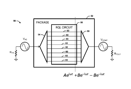
[0022] FIG. 3 illustrates an example of a microwave circuit 50 that
provides for
the generation of a compensation signal for mitigating the effects of
reflections in the
microwave circuit 50. The microwave circuit 50 includes a superconducting
circuit
package 52 that receives an AC input signal from an AC input source (VAC). The
-6-
CA 02982474 2017-10-11
WO 2016/178822 PCT/US2016/028456
superconducting circuit package 52 includes a power splitter 54, a RQL circuit
56
having a plurality of superconducting transmission lines 60 and other
superconducting
circuitry (e.g., bias inductors), and a power combiner 58. The superconducting
circuit
package 52 can be a printed circuit board that resides in a cold space that
maintains the
superconducting circuit package 52 at cryogenic temperatures as stated above.
The
AC source VAC is terminated by an input termination resistor RTIN, which both
reside
outside the cold space, for example, in a room temperature environment It is
not a
requirement to source terminate the AC source VAC.
[0023] The AC source VAC provides an AC input signal to an input of the
power
splitter 54 that splits the AC input signal into a plurality of AC
intermediate signals that
are applied to inputs of corresponding superconducting transmission lines 60
of the
RQL circuit 56. The AC input signal can be a clock input that provides both
power and
clocking functions to the RQL circuit 56. The plurality of AC intermediate
signals
propagate through respective transmission lines of the plurality of
transmission lines 60
to respective outputs coupled to inputs of a power combiner 58. The power
combiner 58 combines the plurality of AC intermediate signals into a single
combined
AC output signal to be terminated by an output termination resistor (R-rouT)
that resides
outside the cold space in, for example, a room temperature environment.
[0024] However, reflections from the transitions from the AC input source
VAC to
the power splitter 54, reflections from the superconducting transmission lines
60 to the
power combiner 58 and reflections from the power combiner 58 to the output
termination resistor R-rouT cause reflections. In particular, the reflections
from the power
combiner 58, as shown by the dashed lines, cause standing waves in the RQL
circuit 56, which directly decreases operating margins in the RQL circuit 56.
The
standing wave consists of the desired forward traveling wave of amplitude A,
and the
undesired backward traveling wave of amplitude B, as shown in the equation of
the AC
input signal at the dashed line location of the superconducting transmission
lines 60 of
the RQL circuit 56, Aeiwt + Bet.
[0025] A second waveform generator (Vamp) is provided that is coupled in
series
with the output termination resistor (R-rouT). The second waveform generator
VCOMP can
be used to produce a compensation signal that is equal and opposite to the
reflections
-7-
CA 02982474 2017-10-11
WO 2016/178822
PCT/1JS2016/028456
in the RQL circuit 56, with correct adjustment of phase and amplitude. For
example, the
second waveform generator VCOMP can produce a compensation signal of amplitude
¨B,
such that the total signal is equal to Ae"t + Be-t,
such that the second and
third terms cancel, thus cancelling the reflections in the RQL circuit 56. The
compensation signal can be a waveform that is at the same frequency as the AC
input
signal, and has an amplitude that is estimated to be an inverted version of a
total sum of
all signal reflections associated with transitions within and outside the
superconducting
circuit. This produces substantially perfect traveling waves through the RQL
circuit 56
irrespective of the number and size of discontinuities in the transitions in
the microwave
circuits 50. The only requirement is that there are no discontinuities in the
region of the
active RQL circuit 58 itself.
[0026] FIG. 4 illustrates another example of a microwave circuit 70 that
provides
for the generation of a compensation signal for mitigating the effects of
reflections in the
microwave circuit 70. The microwave circuit 70 includes a superconducting
circuit
package 72 that resides in a cold space and an AC source (VAC) coupled to an
input of
the superconducting circuit package 72. The AC source VAC resides outside the
cold
space, for example in a room temperature environment, and provides an AC input
signal (e.g., a clock signal) to an input of the superconducting circuit
package 72. The
AC source VAC is source terminated by an input termination resistor RTIN. It
is not a
requirement to source terminate the AC source VAC. The superconducting circuit
package 72 includes an input coaxial cable 74 that receives the AC input
signal VAC and
provides it to a power splitter 76 that generates a plurality of AC
intermediate input
signals each being propagated along respective superconducting transmission
lines of a
plurality of superconducting transmission lines 78.
[0027] The superconducting circuit package 72 includes a plurality of RQL
circuits 80 (e.g., RQL integrated circuits). A set of the plurality of RQL
circuits are
coupled to corresponding superconducting transmission lines, such that an AC
intermediate input signal can be provided to a different set of ROL circuits
80. Each of
the ROL circuits 80 can also have one or more superconducting transmission
lines and
other superconducting circuitry (e.g., bias inductors), such that the
corresponding AC
intermediate input signal can be employed as a clock and power for that
particular ROL
-8-
CA 02982474 2017-10-11
WO 2016/178822 PCT/US2016/028456
circuit 80. The superconducting circuit package 72 also includes a power
combiner 82
that includes inputs for receiving output of the plurality of superconducting
transmission
lines 78. The power combiner 82 combines the plurality of AC intermediate
signals into
a single combined AC output signal that is provided to an output coaxial cable
84 on the
superconducting circuit package 72. An output of the output coaxial cable 84
is
provided to an output termination resistor RTOUT that resides outside the cold
space in,
for example, a room temperature environment.
[0028] A second waveform generator (Vcomp) is provided that is coupled in
series
with the output termination resistor RTOUT. The second waveform generator Vamp
can
be used to produce a compensation signal that is equal and opposite to the
reflections
produced in the RQL circuits 80, with correct adjustment of phase and
amplitude. For
example, the second waveform generator VCOMP can produce a compensation signal
of
amplitude ¨B, such that the total signal is equal to Aeiwt+ Be-t, such that
the
second and third terms cancel, thus cancelling the reflections in the RQL
circuit 80. The
compensation signal can be an AC waveform that is at the same frequency as the
AC
input signal, and has an amplitude that is estimated to be an inverted version
of a total
sum of all signal reflections associated with transitions within and outside
the
superconducting circuit. This produces substantially perfect traveling waves
through the
RQL circuit 80 irrespective of the number and size of discontinuities in the
transitions in
the superconducting circuit package 72 and in the microwave components. The
only
requirement is that there are no discontinuities in the region of the active
circuits.
[0029] The example shown in FIG. 4 involves a transition from a coaxial
cable to
stripline, a power splitter that may be multiple levels deep and include a
Hybrid to
generate I & 0 waveforms from a single input, and many RQL integrated circuits
which
may be mounted on multiple printed circuit boards. Again, traveling waves can
be
produced using a single source at the output to cancel reflections, with the
only
requirement that there are no discontinuities in the region of the active
circuits.
[0030] In view of the foregoing structural and functional features
described
above, an example methodology will be better appreciated with reference to
FIG. 5.
While, for purposes of simplicity of explanation, the methodology of FIG. 5 is
shown and
described as executing serially, it is to be understood and appreciated that
the present
-9-
CA 02982474 2017-10-11
WO 2016/178822 PCT/US2016/028456
invention is not limited by the illustrated order, as some actions could in
other examples
occur in different orders and/or concurrently from that shown and described
herein.
[0031] FIG. 5 illustrates a flow diagram of a method of compensating for
discontinuities in a microwave circuit. The method begins at 110 where an AC
input
signal is applied to an input of a superconducting circuit, such as the
superconducting
circuits illustrated in FIG. 3 or FIG. 4. The superconducting circuit resides
in a cold
space and can include a power splitter that splits the AC input signal into a
plurality of
AC intermediate inputs signals over a plurality of superconducting
transmission lines,
such as those that provide clocking and power to one or more ROL circuits. The
superconducting circuit can also include a power combiner that combines the
plurality of
AC intermediate inputs signals from the outputs of the plurality of
superconducting
transmission lines to a single AC output that is provided at the output of the
superconducting circuit and terminated by a termination resistor that resides
outside the
cold space in, for example, a room temperature environment. The methodology
then
proceeds to 120.
[0032] At 120, a compensation signal is applied at the output of the
superconducting circuit. The compensation signal can be an AC waveform that is
at the
same frequency as the AC input signal, and has an amplitude that is estimated
to be an
inverted version of a total sum of all signal reflections associated with
transitions within
and outside the superconducting circuit. The methodology then proceeds to
adjust the
compensation signal setting at 130, for example, by providing an initial
amplitude of the
compensation signal. The methodology then proceeds to 140 to measure one or
more
operating parameters associated with the operation of the superconducting
circuit. For
example, measurements can be made at different points on the superconducting
circuit
to determine if the plurality of AC intermediate signals have similar
amplitudes at
different physical locations on the superconducting circuit. Alternatively,
the functional
operation of the superconducting circuit could be verified by applying
stimulus to the
superconducting circuit and looking at outputs of the superconducting circuit
to verify
functional operations or failure of operations that may be a result of
reflections. It is to
be appreciated that a variety of techniques can be employed to determine the
operating
margins of the one or more operating parameters of the superconducting
circuit.
-10-
CA 02982474 2017-10-11
WO 2016/178822 PCT/US2016/028456
[0033] The methodology then proceeds to 150 to determine whether or not the
optimal setting of the compensation signal has been achieved. If the optimal
setting of
the compensation signal has been achieved (YES), then the methodology proceeds
to 160 to set the compensation signal at the optimal setting for normal
operations of the
superconducting circuit. If the optimal setting of the compensation signal has
not been
achieved (NO), the methodology returns to 130 to adjust the compensation
signal
setting. The methodology then repeats the measuring of one or more parameters
at 140 and the determining if the optimal setting has been achieved at 150,
until an
optimal setting has been achieved. For example, the compensation signal
setting can
be the amplitude of the compensation signal which can be increased as the
operating
margins of the superconducting circuit increase, until the operating margins
begin to
decease. The amplitude of the compensation signal can be set to its original
value and
decreased to determine if the operating margins of the superconducting circuit
increase,
until the operating margins begin to decease again upon decreasing amplitude.
The
amplitude that provides for the most desirable operating margins can be
determined as
the optimal setting, and thus the value used for normal operations of the
superconducting circuit.
[0034] What have been described above are examples. It is, of course, not
possible to describe every conceivable combination of structures, components,
or
methods, but one of ordinary skill in the art will recognize that many further
combinations and permutations are possible. Accordingly, the invention is
intended to
embrace all such alterations, modifications, and variations that fall within
the scope of
this application, including the appended claims. Where the disclosure or
claims recite
"a," "an," "a first," or "another" element, or the equivalent thereof, it
should be
interpreted to include one or more than one such element, neither requiring
nor
excluding two or more such elements. As used herein, the term "includes" means
includes but not limited to, and the term "including" means including but not
limited to.
The term "based on" means based at least in part on.
-11-