Note: Descriptions are shown in the official language in which they were submitted.
CA 02982871 2017-10-05
1 /65
PROGRAMMABLE MEMORY TRANSFER REQUEST PROCESSING UNITS
Field of the invention
The invention relates, but is not limited, to the implementation and use of so
called memory
protection units, memory management units, instruction caches, data caches,
and caches in the
form of translation lookaside buffers that are used in memory management
units. Various
embodiments of the present invention are suitable for use in many 32-bit and
64-bit processor
environments. This includes, but is not limited, to real-time, safety and
security critical, cyber-
physical computing environments as well as highly resource constrained
computing
environments.
Background of the invention
A reference in this specification to a published document is not to be taken
as an admission that
the contents of that document are part of the common general knowledge of the
skilled addressee
of the present specification. Examples of memory management architectures are
disclosed in
[1], [2], and [3]. The technical terms employed to describe the architecture
of various memory
protection unit (MPU) and memory management unit (MMU) technologies sometimes
have
conflicting definitions. Throughout this specification, including the claims:
= 'Comprises' and 'comprising' are used to specify the presence of stated
features,
integers, steps or components but do not preclude the presence or addition of
one or
more other features, integers, steps, components.
= A memory store (e.g. 118 of figure 1) coupled with a memory controller (e.g.
115 of
figure 1) may be described at a higher level of abstraction as a memory store.
= A peripheral may (e.g. network controller 105 of figure 1) or may not
(e.g.
cryptographic accelerator module) have external 1/0 pins. A peripheral
comprises at
least one interconnect interface, in which each interconnect interface is
either an
interconnect-master or interconnect-target port.
= A bus is a type of interconnect. A crossbar is a type of interconnect.
= A memory-to-memory direct memory access (M2M DMA) unit (e.g. 140 of
figure 1) is
a programmable hardware circuit specifically optimised for issuing memory
transfer
requests over one or more interconnect-master ports (e.g. 143 and 144 of
figure 1) for
the purpose of reading the value of memory stored in one memory location and
writing
that value to a different memory location. A M2M DMA is a slave device subject
to
CA 02982871 2017-10-05
=
2 / 65
control by a different master device (e.g. 110 or 194 of figure 1). A well
known
example of this type of M2M DMA unit is the Intel 8237A. A M2M DMA unit may
also offer additional memory movement related capabilities, such as reading
contiguous memory locations from a memory store and writing each word of data
to
the same address of a memory mapped peripheral. A M2M DMA unit can be
described as a programmable direct memory access (PDMA) unit.
= A memory protection unit (MPU) receives a memory transfer request
associated with
an input address space and in response generates memory transfer requests
associated
with an output address space. An MPU is characterised in that (a) access
controls may
be applied to one or more regions of the input address space; and (b) the MPU
always
employs an identity transformation between the address of a memory transfer
request
in the input address space and the address of the corresponding memory
transfer
request in the output address space. Some MPU architectures are explicitly
designed
to support the mapping of two or more region descriptors to the same
contiguous
region of the input address space at run-time.
= A memory management unit (MMU) receives a memory transfer request
associated
with an input address space and in response generates a corresponding memory
transfer
request associated with an output address space. An MMU is characterised in
that (a)
access controls may be applied to one or more regions of the input address
space, and
(b) the MMU is adapted to translate the address of a memory transfer request
associated with the input address space and the address of the corresponding
memory
transfer request in the output address space.
= A well-formed memory transfer request is any memory transfer request that
correctly
satisfies the associated interconnect protocol requirements for a memory
transfer
request. The reception of a well-formed memory transfer request implies that
that the
request was not malformed on issue and that the request was not corrupted in
transit.
In many publications describing memory management technologies, a "virtual
address space" is
mapped to a "physical address space". This terminology is unambiguous when
there is a single
level of address translation means for software running on a general purpose
processor that is
employed in a given computer architecture. In this specification we use the
terminology an
"input address space" is mapped to a "translated address space". This later
terminology can be
used consistently for each level of memory address translation means when
considering
computer architectures that have two or more levels of address translation
means. This later
CA 02982871 2017-10-05
3 / 65
terminology can also be used consistently for memory address translation means
that are adapted
to receive memory transfer requests from general purpose processors, graphics
processors and
other types of interconnect-master peripherals.
Throughout this specification, including the claims, we define a page, page
descriptor, frame,
segment, segment descriptor and range descriptor as follows:
= A "frame" of N bytes in length defines a contiguous region of memory in a
translated
address space that is N bytes in length and that starts on an N byte boundary.
= A "page" of N bytes in length defines a contiguous region of memory in an
input
address space that is N bytes in length and that starts on an N byte boundary.
A "page
descriptor" describes a page of memory associated with an input address space.
A
page of memory in an input address space may be mapped to a frame of memory in
a
translated address space.
= A "segment" of N bytes in length defines a contiguous region of memory in
an input
address space that is N bytes in length that starts on an 0 byte boundary. The
allocated
portion of a segment may be less than N bytes in length and may also start at
an
address offset located within that segment. The terminology "a variable length
segment" implies that the length of the allocated port of a segment may vary.
The
allocated portion of a segment may be mapped to a contiguous region of memory
on a
P byte boundary in a translated address space. The value of 0 and the value of
P may
also be different. The relationship between the values of N, 0 and P vary
depending
on the segmentation scheme implementation details. In practice, some computer
architectures are designed to employ means implemented in hardware to prevent
the
allocated portions of two programmable segments overlapping in the input
address
space. Correct operation of other computer architectures may require the
executive
software to ensure that the allocated portions of two programmable segments do
not
overlap in the input address space at run-time. A "segment descriptor"
describes a
segment of memory associated with an input address space.
= A "range descriptor" of N bytes in length defines a contiguous region of
memory in the
input address space that is N bytes in length. A range may be defined by a
lower-
bound address and an upper-bound address, or a lower-bound address and a range
length. If there is no programmable address translation enabled in a given
range
descriptor, a range in the input address spaced is mapped using the identity
transformation to a contiguous region of memory in the output address space. A
range
CA 02982871 2017-10-05
4 / 65
descriptor may start and stop on fine grain boundaries (e.g. 64-byte
granularity) in the
input address space. Alternatively, a range descriptor may start and stop on
coarse
grain boundaries in the input address space (e.g. kibibyte granularity). It is
common
with commercial off the shelf MPU implementations to explicitly permit two or
more
range descriptors, in which those range descriptors do not have programmable
address
translation capabilities, to be associated with overlapping memory regions in
the input
address space.
Throughout this specification, including the claims we define a cache line,
cache block, cache
sub-block and a cache tag as follows:
= A "cache line" is a contiguous region of memory. Traditionally in general
purpose
computer architectures, the length of a cache line ranges from 8-bytes to 32-
bytes. In
principle, a cache line could have the same length as the maximum length of a
page or
a segment. Each cache line is associated with a cache tag. In the context of
cache
lines, a "cache tag" stores metadata about the cache line. That metadata may
include,
but may not be limited to, its address in the input address space and/or its
address in the
translated address space and the status of that cache.
= A "cache block" is a contiguous region of memory subdivided into cache
sub-blocks.
Traditionally in general purpose computer architectures a cache block is
comprised of 2
to 4 cache sub-blocks. Traditionally in general purpose computer
architectures, the
length of a cache sub-block ranges between 8-bytes to 32-bytes. Each cache
block is
associated with a cache tag. In the context of cache blocks, the cache tag
stores
metadata about the cache block. That metadata may include, but may not be
limited
to, its address in the input address space and/or its address in the
translated address
space and the status of the cache sub-blocks.
Throughout this specification, including the claims, we define a "programmable
memory transfer
request processing" (PMTRP) unit and a "region descriptor" as follows:
= A PMTRP unit is adapted to receive and process memory transfer requests
according to
various policies, in which each memory transfer request is associated with a
specific
address space, and each address space is associated with certain policies to
be enforced
by that PMTRP unit. A "region descriptor" is used to associate various
policies with a
specific region of a specific address space associated with a specific PMTRP
unit
instance. For example:
CA 02982871 2017-10-05
/ 65
o a region descriptor may or may not be adapted with one or more access
control
fields;
o a region descriptor may or may not be adapted with one or more address
translation fields; and
5 o a region descriptor may or may not be adapted with fields that
modify the default
behavior of the memory subsystem that receives memory transfer requests issued
by the PMTRP unit (e.g. by adjusting the cache write policy and/or memory
order
policy).
= The region of an address space associated with a region descriptor:
o may or may not be constrained with regards to a specific subset of all
possible
base address offsets within an address space; and
o may or may not be constrained with regards to a specific subset of all
possible
region lengths.
Consequently, the fields of a "region descriptor" can be adapted to implement
a variety of
descriptors. This includes, but is not limited to: page descriptors; segment
descriptors;
translation look aside buffer descriptors; range descriptors without
programmatic address
translation; range descriptors with programmatic address translation; and
cache tags.
Clearly, the specific fields of a given region descriptor are defined
specifically for that region
descriptor instance.
A PMTRP unit is defined independently from the one or more interconnect-
masters that are
adapted to issue memory transfer requests to the one or more interconnect-
target ports of that
PMTRP unit. By way of non-limiting example, a PMTRP unit that implements MMU
functionality may be adapted for use as a private IOMMU for one interconnect-
master peripheral
without loss of generality. Furthermore, a PMTRP unit that implements MIVIU
functionality may
be adapted for use a shared IOMMU that is shared across multiple interconnect-
master
peripherals without loss of generality.
Throughout this specification, including the claims we define a "programmable
region
descriptor" as a region descriptor in which one or more fields of that region
descriptor may be
adjusted programmatically.
Early MIVIU schemes for managing the main memory of computer architectures
were typically
adapted for use with main memories that had small storage capacities.
CA 02982871 2017-10-05
6 / 65
As the storage capacity of physical memory increased, MMU schemes based on
different
principles were employed to overcome various perceived or actual limitations
[1], [2] of those
earlier MMU schemes that were designed for small storage capacities.
To the best of the author's knowledge, all published MMU schemes that support
large input
address spaces with fine grain memory allocation capabilities employ (either
software or
hardware controlled) translation look aside buffers (TLB). Those TLB are used
to cache a
relatively small number of the potentially very large number of region
descriptors that can be
associated with an input address space. Consider the VAX-11/780 architecture
[3]. The VAX-
11/780 MMU scheme requires 8,388,608 region descriptors to allocate the entire
32-bit input
address space [2]. Some implementations of the VAX-11/780 employed a unified
TLB to cache
up to 128 of those up to 8,388,608 region descriptors [2]) in high-speed
memory, and stored the
enabled region descriptors in one or more tables and stored in relatively
slower main-memory
storage. Subsequently, to the best of the author's knowledge, industry
practice has
predominantly focused on employing two (or more) levels of indirection
(indexed schemes, hash
schemes, linked-list schemes) when searching for region descriptors to improve
the management
of a potentially very large number of enabled region descriptors. The industry
trend towards the
use of two or more levels of indirection is apparently to overcome various
technical difficulties
found in the single-level translation architectures such as the VAX-11/780
architecture [2]. To
the best of the author's knowledge, all published implementations of MMU
schemes which
support two or more levels of indirection to access a leaf region-descriptor
in a 32-bit or 64-bit
address space employ a (software or hardware controlled) TLB to accelerate
their performance.
It is well known that the use of a TLB to cache region descriptors in
combination with a data
cache significantly increases the complexity of performing static timing
analysis of software
running on a processor core that has a data cache that is enabled and that has
a TLB capability
that is enabled.
There is a long-felt need for an MMU architecture that has low-latency, high-
throughput,
constant time operation with support for relatively fine-grain memory
allocation in 32-bit and
64-bit input address spaces. In the microcontroller market, there is also a
need to provide a
PMTRP unit that can operate as a memory protection unit (MPU) and also operate
as a MMU to
run commercial high-assurance security-critical real-time operating systems
(RTOS). This is
because many high-assurance RTOS rely on the availability of a hardware MMU
with address
translation capabilities.
There is also a long-felt need for a means to cost effectively accelerate the
re-programming of
region descriptors with lower-latency in a time-analysable way in real-time
environments to
CA 02982871 2017-10-05
7 / 65
support faster task-swapping and improved system performance.
There is also a long-felt need to support two-levels of address translation,
in which each level of
the address translation is under the control of different software (e.g. a
hypervisor controls a first
level of the MMU scheme and an operating system hosted on the hypervisor
controls a second
level of that MMU scheme), that is suitable for use in statically time-
analysable real-time
systems.
In resource constrained environments (such as the Internet of Things) that
must run page based
MMU schemes to support general purpose operating systems such as Linux, there
is also a
compelling market need for an innovative MMU architecture that requires less
hardware circuit
area to implement than conventional page-based MMU and that also supports
faster execution of
software after a user address space context swap.
Preferred embodiments of the present invention provide new and innovative
solutions to the
above mentioned market needs.
Disclosure of preferred embodiments of the invention
There is a long-felt need for a means to cost effectively accelerate the re-
programming of region-
descriptors with lower-latency in a time-analysable way in real-time
environments to support
faster task-swapping and improved system performance.
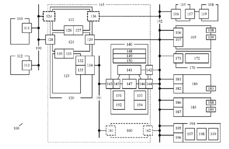
Figure 1 is a block schematic diagram illustrating portions of an apparatus
(100) for processing
data for a preferred embodiment of the present invention. The apparatus (100)
comprises a
processor unit (110). That processor unit (110) has an interconnect-master
port (111) that is
connected to the interconnect (190). Examples of a processor unit include, but
are not limited
to: a general-purpose 16-bit, 32-bit or 64-bit processor core; a graphics
processor unit; or an
application specific processor core. In principle, a interconnect-master
peripheral could be
employed instead of the processor unit (110).
The apparatus (100) further comprises a non-volatile memory store (112). That
non-volatile
memory store (112) is connected by its interconnect-target port (113) to the
interconnect (190).
The apparatus (100) further comprises a programmable memory transfer request
processing
(PMTRP) unit (120). Examples of the functionality a PMTRP unit can implement
include, but
are not limited to: a page based memory management unit (MMU); a page based
MMU with a
translation look aside buffer to cache recently accessed page descriptors; a
segment based MMU;
a segment based MMU with a translation look aside buffer to cache recently
accessed segment
descriptors; a memory protection unit (MPU); and a cache, in which cache tags
and cache data
CA 02982871 2017-10-05
8 / 65
are stored in the programmable configuration data of the memory store (123) of
the PMTRP unit
(120).
A cache tag may comprise, but not be limited to, various of the following
fields: a single-bit
cache line present field; a (32-bit / 64-bit) input address field; a (32-bit /
64-bit) translated
address field; multi-bit fields encoding access control policies for a user
software task; multi-bit
fields encoding access control policies for a system software task; multi-bit
fields encoding
access control policies for a interconnect-master peripheral; a single bit
"cache-line present"
flag; a present mask field with 8, 16 and/or 32 bit granularity; a "cache-line
recently accessed
for read" flag; a single bit "cache-line dirty" flag; a dirty mask field with
8, 16 and/or 32 bit
granularity; a multi-bit cache mode field (e.g. write through, write back, and
so on); a multi-bit
memory order field to indicate memory consistency requirements in multi-bus
master
environments.
The apparatus (100) further comprises:
= A programmable direct memory accessing (PDMA) unit (140).
= An optional unidirectional interconnect bridge (160). The interconnect-
master port
(161) of that bridge (160) is connected to the interconnect (191). The
interconnect-target
port (162) of that bridge (160) is connected to the interconnect (192).
= A SDRAM controller (115). The interconnect-target port (116) of that
SDRAM
controller (115) is connected to the interconnect (192).
= A SDRAM memory store (118). The target port (119) of that SDRAM memory store
(118) is connected to the master port of the SDRAM controller (115).
= An on-chip SRAM memory store (170) with an interconnect-target port (171)
and storage
means (172).
= A network interface peripheral (105). Both the interconnect-target port
(106) and the
interconnect-master port (107) of that network interface peripheral (105) are
connected to
the interconnect (192).
= A High-Definition Multimedia Interface (EIDMI) peripheral (180). Both the
interconnect-target port (181) and the interconnect-master port (182) of that
HDMI
peripheral (180) are connected to the interconnect (192).
= A dual port (188, 189) Universal Serial Bus (USB) peripheral (185). Both the
CA 02982871 2017-10-05
9 / 65
=
interconnect-target port (186) and the interconnect-master port (187) of that
USB
peripheral (185) are connected to the interconnect (192).
= A general purpose processor (194) with integrated core (199), MMU
subsystem (197)
and cache subsystem (199). That general propose processor (194) is connected
via both
the interconnect-master port (195) and the interconnect-target port (196) to
the
interconnect (292).
Collectively, the programmable memory transfer request processing (PMTRP) unit
(120), the
programmable direct memory access (PDMA) unit, the optional bridge (160) and
the
interconnect (191) can be described collectively as a composite programmable
memory transfer
request processing unit (165).
In this pedagogical description, the processor unit (110) is adapted to issue
data memory transfer
requests and/or code memory transfer requests from the interconnect master
(111) to the
interconnect (190).
The programmable memory transfer request processing (PMTRP) unit (120) has a
control unit
(121) which is adapted to access the run-time control unit (122) over a write
port (126) and a
read port (127). The run-time control unit (122) has a bank of one or more
control registers (not
illustrated). The PMTRP unit (120) is adapted to access memory store (123).
The memory
store (123) is adapted to store programmable configuration data for the PMTRP
unit (120). That
programmable configuration data is adapted to store at least two programmable
region descriptor
elements. The control unit (121) is further adapted to receive memory transfer
requests on the
interconnect-target (128) which is connected to the interconnect (190). That
control unit (121)
is further adapted to send memory transfer requests on the interconnect-master
(129) which is
connected to the interconnect (192). The control unit (121) is further adapted
to process a
memory transfer request associated with a first address space received on the
interconnect-target
port (128) in accordance with the at least one policy associated with that
first address space that
are encoded in the at least two or more programmable region descriptor
elements stored in the
programmable configuration data of the memory store (123) at the time of
processing.
The programmable memory transfer request processing (PMTRP) unit (120) has an
interconnect-
target port (134) that is adapted to receive a memory transfer request to
access a portion of the
region descriptor elements stored within the programmable configuration data
stored in the
memory store (123). This includes a read means (132) and a write means (133)
to permit and
process well-formed memory transfer requests that are addressed to a valid
memory location
within that memory store (123) by the interconnect master (143) of the PDMA
unit (140).
CA 02982871 2017-10-05
/ 65
In preferred embodiments of the present invention, the interconnect-target
port (134) of the
programmable memory transfer request processing (PMTRP) unit (120) is also
adapted to
receive a memory transfer request to access a portion of the programmable
configuration data
stored in the memory store (123) that is not a region descriptor.
5 The PMTRP unit (120) has an interconnect-target port (124) that is
adapted to receive read and
write memory transfer requests to the run time control unit (122). That
interconnect-target port
(124) is connected to the interconnect (190). Alternatively, the PMTRP unit
(120) has an
interconnect-target port (136) that is adapted to receive read and write
memory transfer requests
to the run time control unit (122). That interconnect-target port (136) is
connected to the
10 interconnect (192).
The programmable direct memory access (PDMA) unit (140) has a first
interconnect-master port
(143) that is connected to the interconnect (191), a second interconnect-
master port (144) that is
connected to the interconnect (192) and an interconnect-target port (142) that
is connected to the
interconnect (192). The PDMA unit (140) is adapted to employ a bidirectional
FIFO module
(147). The first port of that FIFO unit (147) is connected to a first sub
control circuit (145).
The second port of that FIFO unit (147) is connected to a second sub control
unit (146). The
first sub control circuit (145) is adapted to issue memory transfer requests
to the interconnect-
master (143) and employs a counter (151) and a current memory address index
(152). The
second sub control circuit (146) is adapted to issue memory transfer requests
to the interconnect-
master (144) and employs a counter (153) and a current address index (154).
The PDMA unit (140) is adapted to be programmed by one or more memory transfer
requests
received on the interconnect-target port (142). In this pedagogical
illustration, the PDMA unit
(140) has one programmable memory-to-memory transfer descriptor (148, 149,
150). That
memory-to-memory transfer descriptor (148, 149, 150) has three fields: a
source memory
address field (148), a target memory address field (149) and a memory transfer
length field
(150). The memory-to-memory transfer descriptor is programmed by writing to
fields (148)
then (149) and then (150) in that order.
The PDMA unit's (140) memory-to-memory transfer operation begins after all
three fields (148,
149, 150) of the memory-to-memory transfer descriptor are written to. This
operation is
performed as follows. The value of the source address (148) is loaded into the
current address
pointer (151, 153) of one of the two sub control circuits (145, 146). The
target address (149) is
loaded into the current address pointer (151, 153) of the other one of the two
sub control circuits
(145, 146). For example, the high-bit of the source address (148) could be
used to indicate
which master port (143, 144) of the PDMA unit (140) that source address is
associated with.
CA 02982871 2017-10-05
11 / 65
Alternatively the PDMA unit (140) is adapted to compare the source address
against the different
memory address ranges associated with each of its master ports (143, 144) to
determine which
master port that source address is associated with. The value of the memory
transfer length field
(150) is then copied into both of the counter fields (151, 153). The FIFO unit
(147) is reset to
ensure there are no elements of data present in the queue of that FIFO unit.
The two sub control
circuits (145, 156) are then instructed by the control unit (141) to start
read or writing as required
to successfully execute the requested memory-to-memory transfer operation. The
words of
memory read from the source address are pushed into the FIFO unit (147). The
words of
memory to be written into the target address are popped out of the FIFO unit
(147). The value
of the counters (251) and (253) are decremented according to the amount of
data read or written
respectively. The process for the sub-control unit (145) completes when the
value of its counter
field (151) is zero. The process for the sub-control unit (146) will complete
when the value of
its counter field (153) is zero.
Figure 2 is a block diagram (200) illustrating the partitioning of an address
space (201) for
accessing the programmable configuration data that is stored in the memory
store (123) of the
PMTRP unit (120) illustrated in figure 1 according to a preferred embodiment
of the present
invention. That memory address space (201) is divided into 12 fields (210 to
221). Each field
(210 to 221) is 32-bits in length. That address space (201) is logically
partitioned into:
= a first contiguous set (202) of 6 fields (210 to 215) associated with the
configuration of
the system part of the address space of the target port (128) of the PMTRP
unit (120); and
= a second contiguous set (203) of 6 fields (216 to 221) associated with
the configuration of
the user portion of the address space of the target port (128) of the PMTRP
unit (120).
Field (210) stores configuration and/or state information associated with the
system address
space (202). Fields (211) to (214) are adapted to store at least one region
descriptor associated
with the system address space. The PMTRP unit (120) is adapted such that
writing any value to
the fields (210) to (214) notifies the PMTRP control unit (121) that the
configuration data for the
system portion (202) of the address space is currently being re-programmed.
The PMTRP unit
is adapted such that writing any value to field (215) notifies the PMTRP
control unit (121) that
the configuration data for the system portion of the address space has
finished being re-
programmed.
Field (216) stores configuration and/or state information associated with the
user address space
(203). Fields (216) to (221) are adapted to store at least one region
descriptor associated with
the user address space. The PMTRP unit (120) is adapted such that writing any
value to the
CA 02982871 2017-10-05
12 / 65
fields (216) to (221) notifies the PMTRP control unit (121) that the
configuration data for the
user portion (203) of the address space is currently being re-programmed. The
PMTRP unit
(120) is adapted such that writing any value to field (221) notifies the PMTRP
control unit (121)
that the configuration data for the user portion of the address space has
finished being re-
programmed.
This novel configuration of the address space (201) of the programmable
configuration data
stored in the memory store (123) of the PMTRP unit (120) permits: all of the
system data to be
updated using a contiguous memory-to-memory transfer operation (over fields
210 to 215); all of
the user data to be updated using a contiguous memory-to-memory transfer
operation (over fields
216 to 221); and all of both the system data and user data to be updated using
a contiguous
memory-to-memory transfer operation (over fields 210 to 221).
Advantageously this permits very fast re-programming of the configurable data
of the PMTRP
unit (120) by the PDMA unit (140) in a novel way.
In a further preferred embodiment of the present invention, when the apparatus
(100) is reset, the
PMTRP unit (120) resets the state of its run-time control unit (122) and
resets the state of its
programmable configuration data (123). Furthermore, the default mode of
operation for the
PMTRP unit (120) is to relay memory transfer requests received on the target
port (128) without
modification to the master port (129) and to relay memory transfer responses
receive on the
master port (129) without modification to the target port (128). The PMTRP
unit is then ready
to receive memory transfer requests on port (124), (136) and (134) to
configure its operation.
Figure 3 is a flow chart (300) illustrating a memory-to-memory transfer
operation performed by
the PDMA unit (140 of figure 1) to program all of the of the programmable
configuration data
stored in the memory store (123 of figure 1) of the PMTRP unit (120 of figure
1) in one
memory-to-memory transfer operation (148, 149, 150 of figure 1). In this
example the
processor module (110 of figure 1) is a processor core. The PMTRP unit (120 of
figure 1)
implements the functionality of a memory management unit. In this flow chart,
the PMTRP unit
(120) and processor core (110) are already initialised.
Label (301) illustrates a sequence of steps (301, 305, 308, 311, 314, 330,
331, 334) performed by
the processor core (110). Label (302) illustrates a sequence of steps (302,
306, 309, 312, 315,
321, 323, 327, 328, 329, 332, 335) performed by the PMTRP unit (110). Label
(303) illustrates
a sequence of steps (303, 307, 310, 313, 316, 317, 320, 322, 326, 336)
performed by the PDMA
unit (140). Label (304) illustrates a sequence of steps (304, 318, 319, 324,
325, 337) performed
by the SDRAM store (115, 118).
CA 02982871 2017-10-05
13 / 65
The flow chart (300) starts on steps (301), (302), (303), and (304).
In step (305) the processor core (110) issues a 32-bit write memory transfer
request addressed to
the "source memory address" field (148) of the PDMA unit (140). That memory
transfer
request is received on the target port (128) of the PMTRP unit (120) in step
(306). The PMTRP
unit (120) processes that memory transfer request according to the memory
translation address
policies that are associated with that target port (128) and that are stored
in programmable
configuration data stored in the memory store (123). The PMTRP unit (120) on-
forwards that
processed memory transfer request to the PDMA unit (140) over the master port
(129) and then
over the interconnect (192). The PDMA unit (140) then receives that memory
transfer request
on its target port (142) in step (307). The PDMA unit (140) writes the data
field of that memory
transfer request into its "source memory address" field (148)
In step (308) the processor core (110) issues a 32-bit write memory transfer
request addressed to
the "target memory address" field (149) of the target port (142) of the PDMA
unit (140) That
memory transfer request is processed and on-forward by that PMTRP unit (120)
to the PDMA
unit (140) in step (309). In step (310), that PDMA unit (140) receives that
memory transfer
request and writes the data of that memory transfer request into its "target
memory address" field
(149).
In step (311) the processor core (110) issues a 32-bit write memory transfer
request addressed to
the "memory transfer length" field (150) of the PDMA unit (140). That memory
transfer
request is processed and on-forward by the PMTRP unit (120) to the PDMA unit
(140) in step
(312). In step (313), that PDMA unit (140) receives that memory transfer
request and writes the
data of that memory transfer request into its "length memory address" field
(150). A memory-
to-memory transfer operation is initiated when the memory transfer length
field (250) is written
to.
In step (314) the processor core (110) issues a read memory transfer request
addressed to a
memory location within the address space of the target port (124) of the PMTRP
unit (120) that
will result in that PMTRP unit (120) issuing a read-response after both the
system and user
portion of the programmable configuration data of that PMTRP unit have been
completely
updated. That memory transfer request is received and processed in step (315).
The
corresponding memory transfer response will be issued in step (329) below.
In step (316) the value of the "source memory address" (148) is loaded as the
value of the
current address pointer (153). The value of the "target memory address" (149)
is loaded as the
value of the current address pointer (151). The value of the "memory transfer
length" (150) is
CA 02982871 2017-10-05
14 / 65
loaded as the value of the counter field (151) and the value of counter field
(153). The FIFO
unit (147) is reset to ensure there are no elements of data present in the
queue of that FIFO unit.
The sub-control circuit (145) is instructed to start the process of reading
data from the source
memory. The sub-control circuit (146) is instructed to start the process of
writing data to the
target memory.
In step (317) the sub-control circuit (146) issues a burst memory read memory
transfer request
over port (144) to read the first half of the requested message length (150).
A burst memory
transfer request is memory transfer request that is adapted to operate on two
or more words of
data. That burst read memory transfer request uses the value of the "current
address pointer"
(151). That read burst memory transfer request is received and processed by
the SDRAM store
in step (318). The requested data is issued by the SDRAM store back to the
master port (144) of
the PDMA unit (140) in the form of a burst memory transfer response in step
(319).
In step (320) the PDMA unit (140) receives a read burst memory transfer
response on master
port (144) which contains the requested data. That data is pushed into the
FIFO unit (147).
The value of the "current address pointer" (154) is increased, and the value
of the counter (153)
is decreased according to the amount of data received.
In step (320) the sub control unit (145) pops that data out of the FIFO unit
(147) and issues a
write burst memory transfer request addressed to the target port (134) of the
PMTRP unit (120)
using the value of the "current address pointer" (152). The value of the
"current address
pointer" (151) is increased, and the value of the counter (152) is decreased
according to the
amount of data written.
In step (321) the PMTRP unit (120) receives that burst write memory transfer
request on the
target port (134) and writes the data it receives into the programmable
configuration data stored
in the memory store (123). The PMTRP control unit (121) actively tracks when
the system and
user portions of the programmable configuration data stored in the memory
store (123) are being
updated, and actively tracks when the configuration of the system and user
portions of that
programmable configuration data are finalised as described in the text
describing figure 2.
In step (322) the PDMA unit (140) has received all the data requested by its
burst memory read
memory transfer request issued in step (317). The sub-control circuit (146)
issues a burst
memory read memory transfer request over port (144) to read the second half of
the requested
memory length (150). That burst read memory transfer request uses the value of
the "current
address pointer" (151).
In step (322) the sub control unit (145) of the PDMA unit (140) continues to
on-forward any
CA 02982871 2017-10-05
15 / 65
outstanding data stored in the FIFO unit (147) to the PMTRP unit (120). This
may or may not
involve issuing additional write memory transfer requests as required.
In step (324) the read burst memory transfer request issued in step (322) is
received and
processed by the SDRAM store. In step (325) the requested data is issued by
the SDRAM store
back to the master port (144) of the PDMA unit (140) as burst memory transfer
response.
In step (326) the PDMA unit (140) continues to on-forward data to the PMTRP
unit (120). The
sub control circuit (146) of the PDMA unit (140) stops when the value of it
its counter (153) is
zero. The sub control circuit (145) of the PDMA unit (140) stops when the
value of it its
counter (151) is zero. When both sub control circuits (146) and (145) stop the
PDMA unit's
(140) memory-to-memory transfer operation has completed (at least as far as
that PDMA unit is
concerned).
In step (327) the PMTRP unit (120) continues to receive and process the write
memory transfer
data as issued by the master port (143) of the PDMA unit (140).
In step (328) the PMTRP unit (120) has been successfully re-programmed. The
PMTRP unit
(120) will now service memory transfer requests received on the target port
(128) of the PMTRP
unit (120) according to the policies that are now encoded in the programmable
configuration data
of the memory store (123) of that PMTRP unit.
In step (329) the run-time control unit (122) of the PMTRP unit (120) sends a
read memory
transfer response with the value 1 in the read data field back to the
processor core (110). This
notifies the processor core that the PMTRP unit (120) has been fully re-
programmed. In step
(330) the processor core (110) receives that memory transfer response.
In step (331) the processor core (110) issues a write memory transfer request
addressed to the
input address space of the target port (128) of the PMTRP unit (120). In step
(332) that write
memory transfer request is received on the target port (128) of the PMTRP unit
(120) and
processed by its control unit (121) according to the policies that are
currently stored in the
programmable configuration data stored in the memory store (123) of that PMTRP
unit.
The flow chart stops on labels (334), (335), (336), and (337).
In an alternate preferred embodiment of the present invention: the PMTRP unit
(120) of figure 1
is tightly coupled with the processor core (110) of figure 1; the memory store
(112) of figure 1 is
decoupled from the interconnect (190) of figure 1 and coupled to the
interconnect (192) of figure
1; the bus target (124) of the PMTRP unit (120) figure 1 is not employed; and
the bus target
(136) of the PMTRP unit (120) figure 1 is employed.
CA 02982871 2017-10-05
16 / 65
There is a long-felt need for an MMU architecture that has low-latency, high-
throughput,
constant time operation with support for relatively fine-grain memory
allocation in 32-bit and
64-bit input address spaces.
Figure 4 is a hybrid block schematic diagram and data flow diagram partially
illustrating a
preferred embodiment of the present invention in which the PMTRP unit (120) of
figure 1 is
adapted to implement the functionality of a memory management unit (MMU).
That MMU (120) employs an innovative single-level direct indexed segment based
memory
address translation scheme that is adapted for use with large input address
spaces (e.g. in this
case, a 31-bit input address space (414)) in which there are a small number of
segment
descriptors associated with the input address space (414), and each of the
segments descriptors
support fine-grain memory allocation (533) within that segment. This
innovative memory
address translation scheme is intended for use with a range of memory
organisation schemes
including, but not limited to, those described with reference to figure 6 and
figure 8. In
particular, our innovative memory organisation scheme described with reference
to figure 8
synergistically exploits the combination of: a large input address space; and
(b) a low number of
region descriptors that provide a means for fine-grain memory allocation, to
provide an
unexpected solution to the address space size scaling problem associated with
other single-level
direct indexed memory address translation schemes [1], [2]. Advantageously,
one hardware
implementation of the PMTRP unit (120) can support both of the memory
organisation schemes
described in figure 6 and figure 8.
This scheme can be trivially adapted for use with large input address spaces
that are larger, equal
to, or smaller than the output address space.
The region descriptors of the PMTRP unit (120) are adapted to encode segment
descriptors with
the fields as illustrated for the segment descriptor (430).
Label 410 illustrates the fields of a memory transfer request received on the
interconnect-target
port (128) of the PMTRP unit (120). That memory transfer request (410) is
illustrated with
fields (411), (412) and (414). Field (411) encodes a 3 bit control field for
that memory transfer
request (410). Those three bits encode "read for data", "write" and "read for
execute"
operations respectively. Field (412) encodes a 1 bit privilege value
indicating either system-
level privilege or user-level privilege for that memory transfer request
(410). Field (414)
encodes the value of a 31-bit input address in the input address space. The 5
most significant
bits (415) of the 31-bit input address (414) is employed as the segment index
selector. The
CA 02982871 2017-10-05
17 / 65
remaining 26-bits (416) of the 31-bit input address (414) are employed as a
displacement offset
within that segment (415).
A single-level direct-indexed segment descriptor lookup module (420) stores a
table of 32
segment descriptors that can be programmed at run-time. The segment
descriptors of that table
are indexed at run-time by the top 5 bits (615) of the input address (614) of
the memory transfer
request received on the interconnect-target port (128) of the PMTRP unit
(120).
Each segment descriptor, as illustrated by the segment descriptor (430), is
comprised of 5 fields
(431), (432), (434), (435) and (436). The segment descriptor (430) is a total
of 64-bits in length.
In this embodiment of the present invention, that segment descriptor (430)
supports a 31-bit
input address space that can address 21\31 bytes of storage. That segment
descriptor (430) also
supports a 31-bit output address space that can address 2^31 bytes of storage.
The fields (431 to
436) of the segment descriptor (430) are as follows. Field (431) encodes 6
bits of metadata
associated with that segment descriptor. Field (432) encodes a 29-bit long
displacement offset
within the translated address space. Reducing the number of bits of field
(432) reduces the
physical address space size that the input address space can be mapped to.
This in turn can
reduce the hardware resources required to store the segment descriptors. Field
(434) encodes a
24-bit allocated segment length with 8 byte granularity. Field (433) logically
extends the 24-bit
allocated segment length to a 29-bit allocated segment length value (437).
Specifically, the
binary value zero is stored in each of the top 5 bits (433) of that 29-bit
allocated segment length
value (437). Field (435) encodes a 3-bit permission field for the user
privileged access. Those
three bits encode "read for data", "write" and "read for execute" permissions
respectively. Field
(436) encodes a 3-bit permission field for the system privileged access. Those
three bits encode
"read for data", "write" and "read for execute" permissions respectively.
The output of the segment descriptor lookup module (420) is supplied as input
to the memory
transfer request re-assembly and permission check module (440). That module
(440) comprises
a 29-bit wide arithmetic addition operation which: receives as input the 29
most significant bits
(417) of the 31-bit displacement filed (416) of the memory transfer request
(410); receives as
input the 29-bit displacement offset (432) within the translated address space
for that segment
descriptor (430); and generates a 29-bit value as output that is employed as
the most significant
29-bits (454) of the 31-bit address (454, 454) of the translated memory
transfer request (413).
The memory transfer request re-assembly and permission check module (440)
further comprises
a permission checking module (442) which:
= Checks that the value of the displacement offset (416) of the memory
transfer request
CA 02982871 2017-10-05
18 / 65
(410) is less than or equal to the 29-bit segment length (437) of the segment
descriptor
(430) that is associated with that memory transfer request (410); and
= Checks that the 3 bit control field (411) and 1 bit privilege field (412)
of the memory
transfer request (410) is permitted by the permission policies encoded in the
fields (435)
and (436) of the segment descriptor (430) that is associated with that memory
transfer
request (410). If that permission check fails, a fault signal is issued (443).
In preferred
embodiments of the present invention, that fault signal may result in an
interrupt being
issued to a processor core (110).
The value of the metadata field (431) of that segment descriptor (430) is
employed as the
metadata field (453) of the translated memory transfer request (413). In a
preferred embodiment
of the present invention the meta-data field (431) is adapted to encode:
= A single bit cascade field for conditionally enabling an additional level
of memory
address translation by an additional memory address translation means;
= 4 bits to control the memory subsystem, including: the selection of the
cache mode (e.g.
write through, write back); and the memory order requirements for maintaining
memory
coherency.
The value (413) of the 3 bit operation (411) and 1 bit privilege filed (412)
of the memory transfer
request (410) is supplied as the value of the 3 bit operation (451) and 1 bit
privilege field (452)
of the translated memory transfer request (413) respectively.
The value of the lower 2 bits (418) of the address (416) of the input memory
transfer request
(410) are supplied as the value of the lower 2 bits (454) of the translated
memory request (450).
Figure 5 is a flow chart (500) illustrating the steps of a memory address
translation operation
performed by the control unit (121) of the PMTRP unit (120) according to a
preferred
embodiment of the present invention.
The flow chart starts in step (501).
In step (502) a memory transfer request is received by the control unit (121)
of the PMTRP unit
(120) on port (128).
In step (503) the five most significant bits (415) of the address (414) of
that memory transfer
request (410) are supplied as the index to the segment descriptor lookup
module (420). The
segment descriptor lookup module (420) releases as output the value of the
segment descriptor
CA 02982871 2017-10-05
19 / 65
(430) associated with that index value. The output of segment descriptor
lookup module (420)
is received by the reassembly and permission check module (440).
In step (504) the permission checking module (442) performs consistency checks
between the
memory transfer request (414) received in step (502) and the corresponding
segment descriptor
issued in step (503).
In step (505) if the consistency check of step (504) fails then go to step
(506) otherwise go to
step (509).
In step (506) generate a permission check fault event signal on port (443).
In step (507) if the memory transfer request (410) received in step (502) is a
write memory
transfer request then go to step (515) otherwise go to step (508).
In step (508), issue a read memory transfer response. The value zero is stored
in the data field
of that memory transfer response. If the interconnect protocol offers the
capability, return an
error status for that memory transfer request. Go to step (515).
In step (509) perform the 29-bit wide addition operation (441) and assemble
the fields of the
translated memory transfer request (450) as described in the text describing
figure 4.
In step (510) if the memory transfer request received in step (502) is a write
memory transfer
request then go to step (511) otherwise go to step (512).
In step (511) issue the write memory transfer request on master port (129) of
the PMTRP unit
(120). Go to step (515).
In step (512) issue the read memory transfer request on master port (129) of
the PMTRP unit
(120).
In step (513) receive the corresponding read memory transfer response on the
master port (129)
of the PMTRP unit (120).
In step (514) on-forward the results of that read memory transfer response
received in step (513)
on the target port (128) of the PMTRP unit (120).
The flow-chart stops in step (515).
Figure 6 is a block diagram (600) illustrating an example mapping of a segment
based address
translation scheme between an input address space (610) and a translated
address space (630)
according to a preferred embodiment of the present invention. In this diagram
(600), the input
CA 02982871 2017-10-05
20 / 65
address space (610) starts at zero at the top-left corner of the rectangle
(610) and ends at the
bottom-right corner of that rectangle (610). In this diagram (600), the target
address space (630)
starts at zero at the top-left corner of the rectangle (630) and ends at the
bottom right corner of
that rectangle (630). The linear input address space (610) is subdivided into
N=8 partitions of
equal length (611 to 618). In this illustration, the offset of a segment in
the input address space
partition can be mapped into any location of the output address space with 8-
byte granularity
(e.g. label 632). The allocated length of a segment also has 8-byte
granularity (e.g. labels 634,
837, 838).
The segment descriptor for partition (611) is illustrated as allocating the
entire length of that
partition (611) and translating its base-offset into a higher address (631) in
the target address
space (630). The segment descriptor for partition (612) allocates the top
portion of that partition
(612) and translates its base-offset into a higher address (632) in the target
address space (630).
The allocated portions of the first segment (611) and second segment (612) are
contiguous in the
input address space. The segment descriptor for partition (613) allocates no
portion of that
partition. The segment descriptor for (614) allocates the top portion of that
partition (614) and
translates its base-offset into the same address (634) in the target address
space (630).
The segment descriptor for partition (615) allocates no memory of that
partition. The segment
descriptor for partition (616) allocates no memory of that partition.
The segment descriptor for (617) allocates a small region in the top portion
of that partition (617)
and translates its base-offset into a lower address (637) in the target
address space (630). The
segment descriptor for (618) allocates a larger region in the top portion of
that partition (618)
and translates its base-offset into a lower address (638) in the target
address space. In this
illustration, the segment descriptor for partition (617) is adapted with a
permission access policy
that permits user writes to that allocated region of memory, and the segment
descriptor for
partition (618) is adapted with a permission access policy that permits un-
cached user reads to
the same portion of the translated address space.
In this way we can see that all the variable length segments in the input
address space start on a
partition boundary which permits low-latency hardware-efficient indexing of
that segment
descriptor (when compared to employing a table of range descriptors as
illustrated with label 123
of figure 21). The 8-byte granularity of the allocated length of the segment
and the 8-byte
granularity of the displacement offset permits more efficient packing of an
input address space to
a translated memory address space than is possible with 4 kibibyte long pages
as found in many
conventional MMUs. This fine granularity of mapping into the translated
address space is
particularly desirable in embedded micro applications that have highly
constrained memory
CA 02982871 2017-10-05
21 / 65
storage capacities.
Figure 7 is a block diagram (670) illustrating the organisation of the input
address space (701) of
the single-level direct mapped page based scheme for the DEC VAX-11/760
architecture as
described in figure 6-1 of [31 Each page descriptor is mapped to a contiguous
region of 512
bytes of the 32-bit input address space. The input address space (701) is
equally partitioned into
a process space (702) and a system space (702). The user space (702) is
dynamically partitioned
into a first region (710) called "PO" and a second region (711) called "Pl".
Region PO starts at
the top of the user space and grows downwards. Region P1 starts at the bottom
of the user space
and grows upwards. The system space (703) is dynamically partitioned into a
first region (712)
called "system region" and a "reserved region". The system region (712) starts
at the top of the
system space and grows down. This memory organisation was chosen by DEC to
limit the size
of the single-level direct-indexed tables that store the page descriptors for
the three regions (PO,
P1, system region) that support memory address translation [3].
Figure 8 is a block diagram (670) illustrating an innovative organisation of
an input address
space (701) for a single-level direct mapped segment based scheme for
preferred embodiments
of the present invention. In this example let us consider an M-bit input
address space (801)
equally partitioned into N=8 segments (811 to 818). The top 4 segments (811,
812, 813, 814)
are associated with a system space (803) and the bottom 4 segments (815, 816,
817, 818) are
associated with a user space (802).
Where the input-address space is M=32 bits, a single region descriptor can map
512 mebibytes
of the translated address space. The vast majority of real-time embedded
systems have less than
512 mebibytes of physical memory. In this case, those embedded systems could
map the entire
storage capacity of the physical memory to one region-descriptor. This avoids
the need to map
2 or more segment descriptors to access any contiguous region of the physical
memory. Many
safety critical real-time operating systems statically allocate the memory
available to each
application running on that RTOS at power on. This means that many of the
region descriptors
for the system space and each application space of that RTOS instance can be
created statically
before that device is powered on. For example: The executable code of the RTOS
can be
mapped to partition (811) with system privileged read-only permission access.
The BSS, Stacks
and Heap of that RTOS can be mapped to partition (812) with system privileged
read/write
permission access. The segment (813) can map the entire main-memory into a
contiguous
memory region in the input address space to support memory-to-memory copy
functions
executed by the processor core. The segment (814) can be left unmapped at
power on. The
executable code of a first application can be mapped to partition (815) with
user privileged read-
CA 02982871 2017-10-05
22 / 65
only permission access. The BSS, Stack and Heap of that first application can
be mapped to
partition (816) with user privileged read/write permission access. A first
region of memory
shared between the first application and a second application can be mapped
with user privileged
read/write permission access in segment (817). A second region of memory
shared between the
first application and a second application can be mapped with user privileged
read only
permission access in segment (818). This static mapping does not preclude the
ability to also
perform dynamic mapping at run-time.
Increasing the number of region descriptors from N=8 to N=16 supports a
considerably more
nuanced organisation of memory while still maintaining very small region-
descriptor table for
both the system space (802) and user space (803). The full contents of the
region-descriptor
table can be easily stored in on-chip SRAM for low-latency high-throughput
access. Increasing
the size of the input address space from 32 to 64-bits while simultaneously
holding the size of
the target address space constant does not increase the storage requirements
of the region
descriptor table.
This innovative memory organisation (800) that has been co-designed with our
PMTRP unit that
employs an innovative segmentation scheme for large input address spaces
permits constant time
memory address translations with very low circuit area overheads, making it
ideally suited for
resource constrained safety-critical cyber-physi cal applications.
In a preferred embodiment of the present invention, a 4 kibibyte fixed page
based MMU scheme
is employed as the second level of conditionally enabled memory address
translation means.
There is a long-felt need to support two-levels of address translation, in
which each level of the
address translation is under the control of different software (e.g. a
hypervisor controls a first
level of the MMU scheme and an operating system hosted on the hypervisor
controls a second
level of that MMU scheme), that is suitable for use in statically time-
analysable real-time
systems.
Figure 9 is a block diagram (900) illustrating two-levels of memory management
means
according to a preferred embodiment of the present invention. Diagram (900)
illustrates a
PMTRP unit (910) and a MMU (920).
In preferred embodiments of the present invention, the contents of the
programmable
configuration data of the PMTRP unit (910) is controlled by a software
hypervisor running on a
processor core. That processor core issues one or more memory transfer
requests to the target
CA 02982871 2017-10-05
23 / 65
port (911) of the PMTRP unit (910) to configure the programmable configuration
data of that
PMTRP unit (910).
The contents of the programmable configuration data of the MMU unit (920) is
jointly controlled
by the operating system hosted on the hypervisor in a virtual machine and that
hypervisor's
executive software. The operating system running on that software hypervisor
defines the
policies that the operating system requires for its own internal operation.
Those policies are
encoded and written to the target port (912) of the PMTRP unit (910). Then
those policies are
transformed by the policies in the PMTRP unit (910) that are controlled by the
hypervisor's
executive software. Those transformed policies are then written by the PMTRP
unit (910) into
the programmable configuration data of that MMU unit (920).
Specifically, the PMTRP unit (910) is adapted to receive and process memory
transfer requests
received on its target port (912) according to the policies encoded in the
programmable
configuration data of the PMTRP unit (910). Those policies in the programmable
configuration
data of the PMTRP unit (910) encode how to perform a memory address
translation of the one or
more region descriptors that are received on the target port (912) and that
are intended to be
written into the programmable configuration data of the MMU (910) on its
target port (921).
Those transformed policies are then written by the PMTRP unit (910) into the
programmable
configuration data of that MMU unit (920) using target port (921).
For example, the policies encoded in the PMTRP unit (910) may specify a
contiguous region of
the input address space of target port (922) that can be accessed by memory
transfer requests
received on the target port (922) along with a relative offset to translate
all of those addresses
into the translated address space of the master port (923).
The MMU (920) is adapted to receive memory transfer requests on its target
port (922) and
translate their addresses according to the policies encoded in the
programmable configuration
data of that MMU unit (920).
In this way, the memory address translation scheme written into the
programmable configuration
data of MMU (920) is logically equivalent to performing two-levels of memory
address
translation serially (operating system level memory address translation
followed by software
hypervisor level memory address translation). Advantageously, two-levels of
address space
translation can be affected at run time by the MMU (920) with the latency of
performing a single
level of address space translation.
Figure 10 is a block diagram (1000) illustrating various fields that may be
present in a memory
transfer request (1010) and a memory transfer response (1040) according to a
preferred
CA 02982871 2017-10-05
24 / 65
embodiment of the present invention.
With regard to the memory transfer request (1010), the optional field (1011)
encodes a device
group identifier that identifies a group of interconnect-master devices.
Optional field (1012)
encodes the device type (such as a network interface, a graphics processor
unit, and so on).
Optional field (1013) encodes the device identifier. Optional field (1014)
indicates the
coherency policy (such as un-cached, default cache policy, write-only cache,
write-back cache,
and so on) of this memory transfer request. Optional field (1015) encodes the
memory ordering
policy (total store order, relaxed-memory order, partial store order, and so
on). Optional field
(1016) encodes an interconnect lock request flag. Optional field (1017)
encodes a "read for
data" operation. Optional field (1018) encodes a "write" operation. Optional
field (1019)
encodes a "read for execute" operation. Optional field (1020) encodes the
length of this
memory transfer request. Optional field (1021) encodes an address space
identifier associated
with this memory transfer request. Field (1022) encode the address of the
memory to access.
Optional field (1023) encodes the data to write as part of a write memory
transfer request.
Optional field (1024) encodes the byte enable mask for a write memory transfer
request.
Optional field (1025) encodes the privilege level of this memory transfer
request.
With regard to the memory transfer response (1040), the optional field (1041)
encodes a result
code for the associated memory transfer request (1010). The optional field
(1042) encode a 1-
bit value indicating if the read data associated with this response is valid.
The optional field
(1043) stores the read-data associated with a read memory transfer request
(1010). The optional
field (1044) encodes a read byte enable mask.
In a preferred embodiment of the present invention, the PMTRP unit (120) is
adapted with
means to identify the originating interconnect-master that issued a memory
transfer request
received on its target port (128) using one or more fields (1012) of the
memory transfer request
(1010). In a preferred embodiment of the present invention, the PMTRP unit
(120) is adapted
with means to identify the device group of the originating interconnect-master
that issued a
memory transfer request received on its target port (128) using one or more
fields (1011) of that
memory transfer request (1010). In a preferred embodiment of the present
invention, the
PMTRP unit (120) is adapted with means to identify the type of the originating
interconnect-
master that issued a memory transfer request received on its target port (128)
using one or more
fields (1012) of that memory transfer request (1010). In a preferred
embodiment of the present
invention, the PMTRP unit (120) is adapted with means to associate an address
space identifier
with a memory transfer request received on its target port (128) using one or
more fields (1011,
1012, 1013, 1021) of that memory transfer request. In a preferred embodiment
of the present
CA 02982871 2017-10-05
25 / 65
invention the policies encoded in at least one region descriptor the
programmable configuration
data of the PMTRP unit (120) is associated with one or more of the fields
(1011, 1012, 1013,
1016, 1021) of the memory transfer request received on the target port (128).
There is a long-felt need for an MMU architecture that has low-latency, high-
throughput,
constant time operation with support for relatively fine-grain memory
allocation in 32-bit and
64-bit input address spaces. There is also a long-felt need for a means to
cost effectively
accelerate the re-programming of region descriptors with lower-latency in a
time-analysable way
in real-time environments to support faster task-swapping and improved system
performance.
We will now describe a preferred embodiment of figure 1 in which the PMTPR
unit (120) is
adapted with a page based MMU scheme.
Figure 11 is a hybrid block schematic diagram and data flow diagram partially
illustrating a
preferred embodiment (1100) of the present invention in which the PMTRP unit
(120) of figure 1
is adapted to implement the functionality of a partitioned single-level direct
indexed page based
memory management unit (MMU). In this illustration, the PMTRP unit (120)
employs 8
partitions (1151 to 1158). Those 8 partitions (1151 to 1158) can be described
as 8 independent
memory transfer request processing regions. Each of those partitions is backed
by a single-level
direct indexed table of 64 region descriptors. Each of those 512 region
descriptors are variable-
length page descriptors with provide fine grain memory allocation. Each of
those 512 region
descriptors can be stored in one physical memory store.
Label 1101 illustrates the fields a memory transfer request received on
interconnect-target port
(128) of the PMTRP unit (120).
That memory transfer request (410) is illustrated with fields (1106), (1107),
(1102) and (1105).
Field (1106) encodes a 2 bit privilege field with the following 3 privileges:
user privilege for
software, supervisor privilege for software, and access privilege for
interconnect-master
peripherals.
Field (1107) encodes the selection of one of 5 spaces in 3 bits.
Field (1102) encodes a 32-bit input address. The 2 most significant bits
(1110) of the 32-bit
input address (1102) sub divide that address space (1120) into four spaces: a
interconnect-
master private space (1211), a system space (1122), a high user space (1123)
and a low user
space (1124). The next 6 most significant bits (1111) of the 32-bit input
address (1102) sub
divide each of the spaces (1121, 1122, 1123, 1124) into 64 spaces. The
remaining 24 bits
CA 02982871 2017-10-05
26 / 65
(1112) of the 32-bit input address (1102) provide an offset within the top 8
bits (1103) of the 32-
bit input address (1102).
Field (1105) encodes a 3-bit control field for that memory transfer request
(410). Those 3 bits
encode "read for data", "write" and "read for execute" operations
respectively.
The partition selection module (1130) receives as input the value of the
fields (1 1 06), (1107),
(1110) and (1111). The partition selection module (1130) is adapted to:
= Release output (1140) that indicates a fault during partition selection.
= Release output (1131) that indicates if no memory address translation is
required. That
output (1131) being supplied as input to the reassembly and permission check
module
(1170).
= Release output that indicates which partition of the 8 partitions (1151
to 1158) to use for
the translation of the 32-bit address (1102) of the memory transfer request
(1101). That
output being provided as input to the partitioned one-level direct indexed
page descriptor
lookup module (1150).
The partitioned one-level direct page descriptor lookup module (1150) has 8
partitions (8
independent memory transfer request processing regions). Each of those 8
partitions has a table
of 64 page descriptors that can be programmed at run-time. The choice of
partition to employ
when performing a memory address translation is selected at run-time by the
partition selection
module (1130) for each memory transfer request (1101) received on the target
port (128).
In preferred embodiments of the present invention, the mapping of the 5 spaces
(1107) of the
memory transfer request (1101) to the 8 partitions (1151, 1152, 1153, 1154,
1155, 1156, 1157,
1158) of the partitioned one-level direct-mapped page descriptor lookup (1150)
is statically
mapped by the implementation of the partition selection module (1130). This
simple static
mapping can easily be implemented using combinatorial logic with very low
hardware circuit
resources and at very high speed at run-time.
The arrows drawn within the partition selection module (1130) of figure 11
illustrates the
following pedagogical mapping of input spaces and partitions:
= The interconnect-master private space (1121) is not mapped to any of the
8 partitions
(1151 to 1158).
= The system level space (1122) is always mapped to the partition (1158) In
preferred
CA 02982871 2017-10-05
27 / 65
embodiments of the present invention, a fault (1140) is signalled if the
privilege level
(1106) of that memory transfer request (1101) does not have system level
privilege.
= If the value of space selection field (1107) of the memory transfer
request (1101) is 0, the
low user space (1124) is mapped to the partition (1151) and the high user
space (1123) is
mapped to partition (1152). In this way, the entire user space (1123, 1124)
can be
allocated.
= If the value of space selection field (1107) of the memory transfer
request (1101) is 1, the
low user space (1124) is mapped to the partition (1153) and the high user
space (1123) is
mapped to partition (1154). In this way, the entire user space can be
allocated.
= If the value of space selection field (1107) of the memory transfer request
(1101) is 2, the
low user space (1124) is mapped to the partition (1155) and the high user
space (1123) is
not mapped to any partition.
= If the value of space selection field (1107) of the memory transfer
request (1101) is 3, the
low user space (1124) is mapped to the partition (1156) and the high user
space (1123) is
not mapped to any partition
= If the value of space selection field (1107) of the memory transfer
request (1101) is 4,
the low user space (1124) is mapped to the partition (1157) and the high user
space
(1123) is not mapped to any partition.
Software running on a processor core is responsible for:
= mapping the address-spaces managed by an executive system to the 5 spaces
(1107) of
the memory transfer request (1107) managed by the partition selection module
(1130);
= programming the page descriptors of the partitioned one-level direct-
mapped page
descriptor look up module (1150); and
= changing the value supplied to the space selection field (1107) of a
memory transfer
request (1107) during an address-space context swap of that executive system.
The 5 most recently scheduled user applications with low memory storage
requirements running
on an executive system can be mapped to any of the 5 spaces of the partition
selection module
(1130).
Very low-latency task-swapping between those 5 spaces can be achieved by the
executive
system by simply changing the value supplied to the space selection field
(1107) of the memory
CA 02982871 2017-10-05
28 / 65
transfer request (1107). For example, a processor core (110) may be adapted
with a
configuration register that determines the value of the space selection field
(1107) that will be
used by that processor core when it issues memory transfer requests.
The 2 most recently scheduled user applications with high memory storage
requirements running
on an executive system can be mapped to the 2 spaces of the partition
selection module (1130)
that are mapped to two partitions of the page descriptor lookup module (1150).
The page descriptor lookup module (1150) is adapted to release the value of
the selected page
descriptor as input to the reassembly and permission check module (1170)
The reassembly and permission check module (1170) also receives as inputs the
value of the 2
bit privilege field (1106), 3 bit space selector field (1107), the 8 most
significant bits (1103) of
the 32-bit input address, the 24 least significant bits (1112) of the 32-bit
input address and the 3-
bit control field (1105) of the input memory transfer request (1101). The
reassembly and
permission check module is adapted to:
= release a single bit output (1172) that indicates a fault during
processing of a memory
transfer request;
= release the value of the translated memory transfer request as output
(1173); and
= release a single bit cascade output (1171) that indicates an additional
level of memory
address translation is required for the translated memory transfer request.
The translated address space (1190) illustrates that:
= the top quarter (1191) of the translated address space (1190) is associated
one-to-one with
the interconnect-master private space (1211) of the input address space
(1120), and
= the bottom three quarters (1192) of the translated address space (1190)
is associated with
the system space (1122), high user space (1123) and low user space (1124) of
the input
address space (1120).
Figure 12 is a hybrid block schematic diagram and data flow diagram partially
illustrating a
preferred embodiment of the present invention in which the PMTRP unit (120) of
figure 1 is
adapted to implement the functionality of a memory management unit (MMU). That
MMU
employs a single-level direct indexed page based memory address translation
scheme with a
large input address space and a relatively small number of page descriptors.
This scheme can be trivially adapted for use with large input address spaces
that are larger, equal
CA 02982871 2017-10-05
29 / 65
to, or smaller than the output address space.
In this case, the region descriptors of the PMTRP unit (120) are adapted to
encode page
descriptors, as illustrated by the page descriptor (1210). Figure 12 employs
the memory transfer
request (1101) and its fields (1102), (1103), (1104), (1105), (1106), (1107)
and (1129) as
described in the text describing figure 11. Figure 12 also employs the
partition selection module
(1130) and the partitioned one-level direct indexed page lookup module (1129)
and its outputs
(1131), (1140), (1171) and (1172) as described in the text describing figure
11.
Each page descriptor, as illustrated by the page descriptor (1210), is
comprised of 7 fields
(1121), (1212), (1213), (1214), (1215), (1216) and (1217). The page descriptor
(1210) has a
total length of 32-bits. That page descriptor (1210) supports an input address
space of 21'32
bytes and supports output address space of 2"32 bytes. The fields of this page
descriptor (1210)
are as follows:
= Field (1211) is a 1 bit cascade field which indicates if another level of
memory address
translation is required for the memory transfer requests associated with this
page
descriptor.
= Field (1212) encodes a 4 bit value that can encode 12 distinct page
lengths. In this
illustration the page lengths are: 4 kibibytes, 16 kibibytes, 32 kibibytes, 64
kibibytes, 128
kibibytes, 256 kibibytes, 512 kibibytes, 1 mebibyte, 2 mebibytes, 4 mebibytes,
8
mebibytes and 16 mebibytes.
= Field (1213) encodes an 8 bit frame identifier.
= Field (1214) encodes a 12 bit long displacement offset within the frame.
The number of
bits (i.e. 12 bits) corresponds to the number of distinct page lengths (i.e.
12 page lengths)
of field (1212).
= Field (1215) encodes a 3 bit permission field for user privileged
software access. Those
three bits encode "read for data", "write" and "read for execute" permissions
respectively.
= Field (1216) encodes a 2 bit permission field for system privileged
software access.
Those 2 bits encode "read for any purpose" or "write" permissions
respectively.
= Field (1217) encodes a 2 bit permission field for the system privileged
peripheral access.
Those 2 bits encode "read for data" and "write" permissions respectively.
CA 02982871 2017-10-05
30 / 65
The 32-bit address field (1102) of the memory transfer request (1101) is
logically partitioned
into 2 fields:
= The most significant 8 bits (1103) which encodes the page identifier;
= The other 24 bits (1104) of the 32-bit address (1102) encodes the
displacement within
the page (1103). Those 24 bits (11014) are sub-divided into: the 12 most
significant bits
(1201) of the displacement within the page; and the 12 least significant bits
(1202) of the
displacement within the page.
The output of the page descriptor lookup module (1129 of figure 11 and 1129 of
figure 12) is
supplied as input to the memory transfer request re-assembly and permission
check module
(1170 of figure 11 and 1170 of figure 12). That module (1170 of figure 12)
comprises a 12-bit
wide combining operation module (1273) which:
= Receives as input the 12 most significant bits (1201) of the displacement
within the page
(1103) of the memory transfer request (1101).
= Receives as input the 12 bit long displacement offset with the frame
(1214).
= When the value of the passthrough signal (1131) is 1 then:
o the 12 most significant bits (1201) of the displacement within the page
(1103) of
the memory transfer request (1101) is released as output (1286);
otherwise:
o the 12 most significant bits (1201) of the displacement within the page
(1103) of
the memory transfer request (1101) is combined with the 12 bit long
displacement
offset within the frame (1214) and the result of that combination is released
as
output (1286). In preferred embodiments of the present invention a 12-bit wide
arithmetic addition is employed as the combining function. Alternative
combining functions include, but are not limited to: a 12-bit wide XOR; or a
combining function that uses the value of the length field (1212) to determine
which of the bits of field (1201) and which of the bits of (1214) to release
as
output.
The memory transfer request re-assembly and permission check module (1170)
further
comprises a permission checking module (1274) that:
= Checks that the value of the 12 most significant bits (1201) of the
displacement within
CA 02982871 2017-10-05
31 /65
the page (1103) of the memory transfer request (1101) is less than or equal to
the page
length (1212) of the page descriptor (1210) associated with that memory
transfer request
(1101).
= Checks that the control field (1105) and privilege field (1106) of the
memory transfer
request (1101) is permitted by the permission policies encoded in the fields
(1215, 1216,
1217) of the page descriptor (1210) associated with that memory transfer
request (1101).
If that permission check fails, a fault signal is thrown (1172).
In preferred embodiments of the present invention, the activation of either of
the fault signals
(1140) or (1172) results in an interrupt event being issued to a processor
core (110).
The value of the translated memory transfer request (1280) is generated as
follows: The value of
the control field (1281) of the translated memory transfer request (1280) is
set to the value of the
control field (1105) of the input memory transfer request (1101). The value of
the privilege
field (1282) of the translated memory transfer request (1280) is set to the
value of the privilege
field (1106) of the input memory transfer request (1101). The value of the
optional space
selection field (1283) of the translated memory transfer request (1280) is set
to the value of space
selection field (1107) of the input memory transfer request (1101). The value
of the 8-bit frame
field (1284) of the address field (1284, 1285) of the translated memory
transfer request (1205) is
set to the value of the frame field (1103) of the input memory transfer
request (1102) when the
value of the passthrough signal (1131) is 1. Otherwise the value of the 8-bit
frame field (1284)
of the address field (1284, 1285) of the translated memory transfer request
(1280) is set to the
value of the frame identifier (1213) of the page descriptor (1210) associated
with that memory
transfer request (1101). The value of the most significant 12 bits of the 24-
bit displacement
field (1285) of the address field (1284, 1285) of the translated memory
transfer request (1280) is
set to the value of the output (1286) of the 12-bit wide combining operation
module (1273) The
value of the least significant 12 bits of the 24-bit displacement field (1285)
of the address (1284,
1285) of the translated memory transfer request (1280) is set to the value of
the least significant
12 both of the address field (1104) of the memory transfer request (1101).
Figure 13 is a flow chart (1300) illustrating a memory address translation
operation performed
by the control unit (121 of figure 1) of the PMTRP unit (120 of figure 1)
according to preferred
embodiments of the present invention as described in figure 11 and figure 12.
The flow chart starts in step 1301.
In step (1302) a memory transfer request is received (1101) by the control
unit (121) on target
port (128).
CA 02982871 2017-10-05
32 / 65
In step (1303) the partition selection module (1130) processes the memory
transfer request
(1101) to determine which partition, if any, is associated with that memory
transfer request.
Permission checks are performed with regard to memory transfer requests
addressed to system
space (1122). Checks are also performed with regard to memory transfer
requests addressed to
the high user space (1124) and the availability of a partition mapped to that
high user space
(1124)
In step (1304) if a fault is generated during step (1303) then go to step
(1308) else go to step
(1305).
In step (1305), the partition selected in step (1303) is supplied as the
partition index to the
partitioned single-level direct indexed page descriptor lookup module (1150).
The 6 bits (1111)
of the 32-bit address field (1102) of the memory transfer request (11102) that
sub-divide the
divide each of the 4 spaces (1121, 1122, 1123, 1124 of figure 11) into 64
spaces is supplied as
the page index to that partitioned page descriptor lookup module (1150). The
page descriptor
lookup module retrieves the value of the requested page descriptor and
releases that value as
output. The output of page descriptor lookup module is received as input by
the reassembly and
permission check module (1170).
In step (1306) the permission checking module (1274 of figure 12) performs
consistency checks
between the memory transfer address received in step (1302) and the page
descriptor issued in
step (1305).
In step (1307) if the consistency check performed in step (1306) fails then go
to step (1308),
otherwise go to step (1311).
In step (1308) generate a fault signal (on 1140 or 1172)
In step (1309) if the memory transfer request received in step (1302) is a
write request go to step
(1317), otherwise go to step (1310).
In step (1310) issue a read memory transfer response with the value zero in
the data field. If the
interconnect protocol offers the capability, return an error status (1041 of
figure 10) for that
memory transfer request. Go to step (1317).
In step (1311) perform the 12-bit wide merging operation (1273) and generate
the fields of the
translated memory transfer request (1280).
In step (1312) if the memory transfer request received in step (1202) is a
write request go to step
(1313), otherwise go to step (1314).
CA 02982871 2017-10-05
33 / 65
In step (1313) issue the write memory transfer request on master port (129) of
the PMTRP unit
(120). Go to step (1317).
In step (1314) issue the read memory transfer request on master port (129) of
the PMTRP unit
(120).
In step (1315) receive the corresponding read memory transfer response on
master port (129) of
the PMTRP unit (120).
In step (1316) on-forward the results of that read memory transfer response on
the target port
(128) of the PMTRP unit (120).
The flow-chart stops in step (1317).
In highly resource constrained embedded micro environments, there is a need to
reduce the
amount of hardware resources exclusively dedicated to the PMTRP unit (120 of
figure 1). In
particular, in resource constrained environments (such as the Internet of
Things) that must run
page based MMU schemes to support general purpose operating systems such as
Linux, there is
also a long-felt need for an innovative MMU architecture that requires less
hardware circuit area
to implement than conventional page-based MMU and that also supports faster
execution of
software after a user address space context swap. There is also a need to
improve software
performance after a task context switch for MMU schemes that employ
translation look aside
buffers. There is also a long-felt need for a means to cost effectively
accelerate the re-
programming of region-descriptors with lower-latency in a time-analysable way
in real-time
environments to support faster task-swapping and improved system performance.
With reference to figure 12, an alternate preferred embodiment of the present
invention makes
the following modifications:
= The two bit field (1216) and the two bit field (1217) are not employed.
Software with
system privilege is permitted to access all data. Peripherals are permitted to
access to all
data.
= The field 1212 encodes an 8-bit value that can encode 256 bit distinct
page lengths. The
first set of 128 page lengths (with values 0 to 127) have 4 kibibyte
granularity and map
the range from 4 KB to 512 KB. The second set of 128 page lengths (with values
128 to
255) have 128 KB granularity and map the range from 128KB to 16 mebibytes.
CA 02982871 2017-10-05
34 / 65
This alternate configuration provides improved granularity of memory
allocation for the page
descriptor (1210) while maintaining a descriptor length of 32-bits. Most
applications in
resource-constrained embedded micro applications today require less than 512
KB memory, and
so can be efficiently mapped to physical memory with 4KB granularity. When
required, the
granularity of the page-length (1212) and the granularity of the displacement
offset (1214) can
be increased easily by a person skilled in the art.
We will now describe a preferred embodiment of figure 1 in which the PMTPR
unit (120) is
adapted with means to cache access to at least two sets (which may be
implemented as two
tables) of at least two programmable region descriptors by generating and
sending at least one
memory transfer request over the master port (129) of the PMTRP unit (120) and
receiving the
corresponding responses on that master port (129). This specific adaptation
permits cached
region descriptors to be directly stored in the same memory store (170) that
translated memory
transfer requests may be addressed to. In particular, those cached region
descriptor tables can
be used to implement the second-level of a two-level translation look-aside
buffer scheme, in
which the first-level of cached TLB entries is stored in the programmable
configuration data of
the PMTRP unit. Decoupling the second level of TLB entries from the
programmable
configuration data of the PMTRP unit permits each user address space to have
its own dedicated
second-level translation look-aside buffer table stored in the relatively
large and cheap main-
memory, resulting in a higher second-level TLB hit rate after a context swap.
For example, the
first level of the TLB lookup can employ a fully associative lookup of cached
TLB descriptors,
and the second level of the TLB lookup can employ a single-level direct index
lookup of cached
TLB descriptors. In preferred embodiments of the present invention, each
software application
that has a distinct user address space has its own dedicated table of single-
level direct index
lookup of cached TLB descriptors.
Figure 14 is a block diagram illustrating the partitioning of an address space
(1400) for accessing
programmable configuration data stored in the memory store (123) of the PMTRP
unit (120)
according to a preferred embodiment of the present invention. In figure 14,
that memory
address space (1400) is divided into 23 fields (1401 to 1423). Each of the 23
fields (1401 to
1423) is 32-bits in length. That address space (1400) is logically partitioned
into:
= a first contiguous set (1431) of 6 fields (1401 to 1406) associated with the
configuration
of the system part of the address space of the target port (128) of the PMTRP
unit (120);
= a second contiguous set (1432) of 6 fields (1407 to 1413) associated with
the
configuration of the user part of the address space of the target port (128)
of the PMTRP
CA 02982871 2017-10-05
3 5 / 65
unit (120); and
= a third contiguous set (1433) of 10 fields (1414 to 1423) associated with
the
configuration of a cache that caches information associated with either the
system or user
part of the address space of the target port (128) of the PMTRP unit (120).
The first contiguous set (1431) of fields comprises:
= 16-bit long field (1401.a) which encodes the configuration metadata
associated with a
first system region descriptor table. The base address offset of the first
system region
descriptor table is stored in the 32-bit long field (1402).
= 16-bit long field (1401.b) which encodes the configuration metadata
associated with a
second system region descriptor table. The base address offset of the second
system
region descriptor table is stored in the 32-bit long field (1403).
= Field (1404 and 1405) which encodes a second level of address translation
for the system
region. Specifically the field (1404) encodes the maximum length of the system
address
space within the first level of the translated address space and field (1405)
encodes a
displacement offset of the system address space within the second level of the
translated
address space.
The PMTRP unit (120) is adapted such that writing any value to fields (1401,
1402, 1403, 1404,
1405) notifies the PMTRP control unit (121) that the configuration data for
the system portion of
the address space is currently being re-programmed. The PMTRP unit (120) is
adapted such
that writing any value to field (1406) notifies the PMTRP control unit (121)
that the
configuration data for the system portion of the address space has finished
being re-programmed.
The second contiguous set (1431) of fields comprises:
= 16-bit long field (1407.a) which encodes the configuration metadata
associated with a
first user region descriptor table. The base address offset of the first user
region
descriptor table is stored in the 32-bit long field (1408).
= 16-bit long field (1407.b) which encodes the configuration metadata
associated with a
second user region descriptor table. The base address offset of the second
user region
descriptor table is stored in the 32-bit long field (1409).
= Field (1410) is used to assist the executive system calculate the hash
transformation for
associating a region of the input address space with a region descriptor
encoded in a
CA 02982871 2017-10-05
36 / 65
hash-indexed one-level descriptor table. The value to hash is written into the
field
(1410). The hashed value is then read from the field (1410).
= Fields (1411) and (1412) which encodes a second level of address
translation for the user
region. Specifically the field (1411) encodes the maximum length of the user
address
space within the first level of the translated address space and field (1412)
encodes a
displacement offset of the user address space within the second level of the
translated
address space.
The PMTRP unit (120) is adapted such that writing any value to fields (1407,
1408, 1409, 1410,
1411, 1412) notifies the PMTRP control unit (121) that the configuration data
for the user
portion of the address space is currently being re-programmed. The PMTRP unit
(120) is
adapted such that writing any value to field (1413) notifies the PMTRP control
unit (121) that
the configuration data for the user portion of the address space has finished
being re-
programmed.
The third contiguous set (1431) of fields comprises:
= A first 128-bit long cache line ({1415 to 1418}).
= A second 128-bit long cache line ({1419 to 1422}).
= Field (1414) which encodes the tag data for the first cache line ({1415
to 1418}) and the
second cache line ({1419 to 1422}).
The PMTRP unit (120) is adapted such that writing any value to fields (1414,
1415, 1416, 1417,
1418, 1419, 1420, 1421, 1422) notifies the PMTRP control unit (121) that the
configuration data
for the cache is currently being re-programmed. The PMTRP unit is adapted such
that writing
any value to field (1413) notifies the PMTRP control unit (121) that the
configuration data for
the cache has finished being re-programmed.
In a preferred embodiment of the present invention, the cache fields (1433) of
the programmable
configuration data of the PMTRP unit (120) are adapted to implement a
translation look aside
buffer for region descriptors in which:
= the first 128-bit long cache line ({1415 to 14181) is adapted to store a
first 128-bit long
region descriptor; and
= the second 128-bit long cache line ({1419 to 1422}) is adapted to store a
first 128-bit
long region descriptor.
CA 02982871 2017-10-05
37 / 65
In preferred embodiments of the present invention, the two 128-bit long region
descriptors are
used to cache region descriptors associated with the user space or the system
space.
Figure 15 is a block diagram illustrating a 16-bit wide configuration metadata
field (1510)
employed in figure 14 according to a preferred embodiment of the present
invention. That
configuration metadata field (1510) is employed in the fields (1401.a, 1402.b,
1407.a, 1407.b) of
the programmable configuration data stored in the memory store (123) of the
PMTRP unit (120).
The fields of the 16-bit configuration metadata field (1510) comprise:
= A 1 bit long field (1511) indicating if the region descriptor table
associated with this
configuration metadata field is enabled.
= A 1 bit long field (1512) indicating if a linear direct-mapped or non-linear
direct mapped
indexing scheme is employed to access a region descriptor in that table of
region
descriptors.
= A 3 bit long field (1513) encoding the number of region descriptors in
the table. In
preferred embodiments of the present invention, the number of region
descriptors can be
selected from one of the following 8 table lengths: 8, 16, 32, 64, 128, 256,
512 and 1024
region descriptors.
= A 3 bit long field (1514) indicating the encoding format of the region
descriptors. 5
example encoding formats include:
o A table of 32-bit long page descriptors.
o A table of 64-bit long segment descriptors.
o A table of 64-bit long cached paged descriptors.
o A table of 128-bit long cached segment descriptors.
o A table of 32-bit long table descriptors that point to tables of
descriptors.
= A 6 bit long field (1515) indicating the maximum page length or the
maximum segment
length as most appropriate for the type of descriptor. In a preferred
embodiment of the
present invention, the 6-bit binary value 000000 encodes the decimal value 1,
and the 6-
bit value 111111 encodes the decimal value 64. The value of the maximum length
field
is calculated as the value 2 exponentially raised (A) to the power of the
value of decimal
value of that 6-bit field. So if the decimal value of that 6-bit long field is
32, the
maximum length is calculated as (2^32) ---- 4 gibibytes.
CA 02982871 2017-10-05
38 / 65
= A I bit long field (1516) indicating if an additional length check is
employed after the
first address translation operation is completed.
= A 1 bit long field (1517) indicating if a second address translation is
employed after the
first address translation operation is completed.
Figure 16 is a block diagram illustrating a region descriptor (1600) employed
in figure 14
according to a preferred embodiment of the present invention.
When the region descriptor (1600) is configured as a 32-bit long page
descriptor, the fields of
figure 16 are employed as follows: A 1 bit long field (1611) indicating if
this region descriptor
is enabled. A 1 bit long field (1612) indicating if peripherals are
simultaneously permitted "read
for data" and "write" access the region of memory associated with this region
descriptor. A 1
bit long field (1613) indicating if supervisor software is simultaneously
permitted "read for
data", "write" and "read for execute" access the region of memory associated
with this region
descriptor. A 3 bit long field (1614) encoding "read for data", "write" and
"read for execute"
permissions for user software respectively. A 26 bit long field (1615)
encoding the frame
identifier for this page. The fields (1621, 1622, 1623, 1624, 1625, 1631,
1635, 1640) are not
employed.
When the region descriptor (1600) is configured as a 64-bit long segment
descriptor, the fields of
figure 16 are employed as follows: A 1 bit long field (1611) indicating if
this region descriptor
is enabled. A 1 bit long field (1612) indicating if peripherals are
simultaneously permitted "read
for data" and "write" access the region of memory associated with this region
descriptor. A 1
bit long field (1613) indicating if supervisor software is simultaneously
permitted "read for
data", "write" and "read for execute" access the region of memory associated
with this region
descriptor. A 3 bit long field (1614) encoding "read for data", "write" and
"read for execute"
permissions for user software respectively. A 26 bit long field (1615)
encoding the
displacement within the translated address space for this region with 64 byte
granularity. A 26
bit long field (1625) encoding the length of the allocated portion of this
segment with 64 byte
granularity. The fields (1621, 1622, 1623, 1624) are reserved for future use.
The fields (1625,
1631, 1635, 1640) are not employed.
When the region descriptor (1600) is configured as a 64-bit long cached page
descriptor, the
fields of figure 16 are employed as follows: A 1 bit long field (1611)
indicating if this region
descriptor is enabled. A 1 bit long field (1612) indicating if peripherals are
simultaneously
permitted "read for data" and "write" access the region of memory associated
with this region
descriptor. A 1 bit long field (1613) indicating if supervisor software is
simultaneously
CA 02982871 2017-10-05
39 / 65
permitted "read for data", "write" and "read for execute" access the region of
memory associated
with this region descriptor. A 3 bit long field (1614) encoding "read for
data", "write" and
"read for execute" permissions for user software respectively. A 26 bit long
field (1615)
encoding the displacement within the translated address space for this region
with 64 byte
granularity. A 26-bit long field (1625) encoding the page identifier of this
region descriptor
with 64 byte granularity. A 1-bit long field (1621) encoding a data-written
(dirty) flag for this
cached region descriptor. A 1-bit long field (1622) encoding a data-read flag
for this cached
region descriptor. A 1-bit long field (1263) encoding the cache-policy to be
used for memory
transfer requests addressed to a memory location within the region associated
with this region
descriptor. The field (1624) is reserved for future use. The fields (1625,
1631, 1635, 1640) are
not employed.
When the region descriptor (1600) is configured as a 128-bit long cached
segment descriptor, the
fields of figure 16 are employed as follows: A 1 bit long field (1611)
indicating if this region
descriptor is enabled. A 1 bit long field (1612) indicating if peripherals are
simultaneously
permitted "read for data" and "write" access the region of memory associated
with this region
descriptor. A 1 bit long field (1613) indicating if supervisor software is
simultaneously
permitted "read for data", "write" and "read for execute" access the region of
memory associated
with this region descriptor. A 3 bit long field (1614) encoding "read for
data", "write" and
"read for execute" permissions for user software respectively. A 26 bit long
field (1615)
encoding the displacement within the translated address space for this region
with 64 byte
granularity. A 1-bit long field (1621) encoding a data-written (dirty) flag
for this cached region
descriptor. A 1-bit long field (1622) encoding a data-read flag for this
cached region descriptor.
A 1-bit long field (1263) encoding the cache-policy to be used for memory
transfer requests
addressed to a memory location within the region associated with this region
descriptor. The
field (1624) is reserved for future use. A 26-bit long field (1625) encoding
the segment
identifier of this region descriptor with 64 byte granularity. A 26-bit long
field (1635) encoding
the length of the allocated portion of this segment with 64 byte granularity.
The fields (1631,
1640) are reserved for future use.
When the region descriptor (1600) is configured as a 32-bit long table
descriptor, the fields of
figure 16 are employed as follows: A 1 bit long field (1611) indicating if
this region descriptor is
enabled. A 26 bit long field (1615) encoding an address (in the translated
address space) of a
table of region descriptors. The fields (1612, 1613, 1614) are reserved for
future use.
In preferred embodiments of the present invention, N-bit long region
descriptors are N-bit
aligned in memory.
CA 02982871 2017-10-05
40 / 65
Figure 17 is a hybrid block schematic diagram and data flow diagram partially
illustrating an
apparatus (1700) according to a preferred embodiment of the present invention
as described with
reference to figures 1, 14, 15 and 16. Processor core (110) and its master
port (111) of figure 17
are described in the text describing figure 1. The PMTRP unit (120) and its
associated labels
(121, 123, 128, 129, 130, 131, 134, 130) of figure 17 are described in the
text describing figure
1. The apparatus (1700) further comprises: an IRQ target port (1711) on the
core (110); and an
IRQ master port (1728) on the PMTRP unit (120) which is connected to the IRQ
target port
(1711).
The programmable configuration data stored in the memory store (123) of the
PMTRMP unit
(120) is adapted according to the text describing figure 14.
Label (1710) illustrates an input address space equally partitioned into a
system space (1711) and
a user space (1712). Label (1720) illustrates a translated address space.
Memory transfer
requests issued over master port (129) of the PMTRP unit are addressed to that
translated address
space (1720).
Label (1402 of figure 17) illustrates that the base address offset of the
first system region
descriptor table field (1402 of figure 14) is associated with a system region
descriptor table
(1421) that stores 8 region descriptors. The system space (1711) of the input
address space
(1710) of port (128) is associated with the first system region descriptor
table (1421) that is
stored in the translated address space (1720).
Label (1408 of figure 17) illustrates that the base address offset of the
first user region descriptor
table field (1408 of figure 14) is associated with a user region descriptor
table (1422) that stores
8 region descriptors. The user space (1712) of the input address space (1710)
of port (128) is
associated with the first user region descriptor table (1422) that is stored
in the translated address
space (1720).
Label ({1415 to 14181 of figure 17) illustrates that one of the region-
descriptors of the user
region descriptor table (1423) is cached in the first 128-bit long cache line
({1415 to 14181) of
figure 14. In this embodiment, the region descriptor table (1423) stores 16
region descriptors.
The user space (1712) is associated with the user region descriptor table
(1423) that is stored in
the translated address space (1720).
The region (1725) is associated with the region descriptor cached in the first
128-bit long cache
line ({1415 to 1418}). The user space (1712) is associated with the region
(1725) that is stored
in the translated address space (1720).
CA 02982871 2017-10-05
41 /65
In a preferred embodiment of the present invention, the system region
descriptor table (1421) is
configured in one of the 2 following schemes:
= A single-level direct mapped index segment table scheme;
= A single-level direct mapped index cached page table scheme that stores
the region
descriptors for the second level of a two-level TLB scheme.
In a preferred embodiment of the present invention: the region descriptor
table (1422) encodes
the first level of a two-level direct mapped index table scheme; and the
region descriptor table
(1423) encodes the second level of a two-level direct mapped index table
scheme.
In a preferred embodiment of the present invention, the region descriptor for
the first level of a
two-level direct mapped index table scheme and the region descriptor for the
second level of a
two-level direct mapped index table scheme are sequentially loaded into the
same cache line
({1415 to 1418}) during a two-level table lookup operation.
In a further preferred embodiment of the present invention, the control unit
(121 of figure 17) of
the PMTRP unit (120 of figure 17) is adapted with an additional bus master
interface (1729).
The PMTRP unit (121 of figure 17) is further adapted with means to issue two
concurrent
accesses to the translated address space (1720) to read two region descriptor
elements stored in 2
different memory stores concurrently.
Figure 18 is a flow chart (1800) illustrating a memory address translation
operation performed
by the control unit (121 of figure 17) of the PMTRP unit (121 of figure 17)
according to figures
14, 15, 16 and 17. In this pedagogical flow-chart, the PMTRP unit is adapted
only to query
single-level direct-mapped region descriptor tables.
The flow chart starts in step (1801).
In step (1802) a memory transfer request is received by the control unit (121
of figure 17) of the
PMTP unit (120) on target port (128).
In step (1803) the contents of the cache tag data field (1414 of figure 14)
and the contents of the
two 128-bit cache-lines fields ({1415 to 1418}) and ({1419 to 1422}) are
queried to determine
which, if any, of the two 128-bit cache-lines is associated with this memory
transfer request.
In step (1804) if none of the cache-lines are associated with this memory
transfer request, go to
step (1805) otherwise go to step (1809).
In step (1805) the content of the configuration metadata associated with: a
first system region
CA 02982871 2017-10-05
42 / 65
descriptor table (1401.a) of figure 14; a second system region descriptor
table (1401.b); a first
user region descriptor table (1407.a); and a second user region descriptor
table (1407.b) are
queried to determine the base address offset (1402, 1403, 1408, 1409) of the
table of region
descriptors related to this memory transfer request.
In step (1806) a burst read memory transfer request is issued to retrieve the
region descriptor
associated with this memory transfer request from the region descriptor table
selected in step
(1805). The length of the burst memory transfer request is determined in
relation to the type of
region descriptor indicated by the region descriptor encoding scheme field
(1515 of figure 15) of
the configuration metadata associated with this memory transfer request.
In step (1807) the value of the selected region descriptor element is loaded
into the least recently
used cache-line of the two 128-bit cache-lines ({1415 to 1418}) and ({ 1419 to
1422)).
In step (1808) the value of the region descriptor element received in (1807)
is inspected.
In step (1809) if the region descriptor element is not enabled then go to step
(1813). If the
region descriptor is a cached region descriptor that is not related to the
address of the memory
transfer request in step (1802) then go to step (1813). Go to step (1810).
In step (1810) the region descriptor stored in the cache-line associated with
the memory transfer
request received by the control unit on port (128) in step (1802) is received
by the reassembly
and permission check module of that PMTRP unit.
In step (1811) the permission checking module performs consistency checks
between the
memory transfer address received in step and the segment descriptor received
in step (1810).
In step (1812) if the consistency check fails then go to step (1813) otherwise
go to step (1816).
In step (1813) generate a fault notification event by throwing an interrupt on
the port (1728) of
the PMTRP unit (120) of figure 17.
In step (1814) if the memory transfer request received in step (1802) is a
write request then go to
step (1815) otherwise go to step (1820).
In step (1815) issue a read memory transfer response with the value zero in
the data field (1043).
If the interconnect protocol offers an error reporting capability then return
an error status (1041)
for that memory transfer request. Go to step (1822).
In step (1814) perform the memory address translation and generate the fields
of the translated
memory transfer request.
CA 02982871 2017-10-05
43 / 65
In step (1817) if the memory transfer request received in step (1802) is a
write request then go to
step (1818) otherwise go to step (1819).
In step (1818) issue the write memory transfer request on the master port
(1818) of the PMTRP
unit. Go to step (1822).
In step (1819) issue the read memory transfer request on the master port (129)
of the PMTRP
unit.
In step (1820) receive the corresponding read memory transfer response on the
master port (129).
In step (1821) on-forward the results of that read memory transfer response on
the target port
(128).
The flow-chart stops in step (1822).
In a preferred embodiment of the present invention, the steps (1805), (1806),
(1808) and (1809)
are further adapted to retrieve and evaluate two region descriptors. For
example searching the
region descriptors stored in a two-way set associative table of cached region
descriptors. This
adaptation can be easily performed by a person skilled in the art of
implementing set associative
cache schemes.
In a preferred embodiment of the present invention, the steps (1805), (1806),
(1808) and (1809)
are further adapted to perform a two-level region descriptor walk. This
adaptation can be easily
performed by a person skilled in the art of implementing two-level MMU
schemes.
There is a long-felt need for an MMU architecture that has low-latency, high-
throughput,
constant time operation with support for relatively fine-grain memory
allocation in 32-bit and
64-bit input address spaces. In the microcontroller market, there is also a
need to provide a
PMTRP unit that can operate as a memory protection unit (MPU) and also operate
as a MMU to
run commercial high-assurance security-critical real-time operating systems
(RTOS). This is
because many high-assurance RTOS rely on the availability of a hardware MMU
with address
translation capabilities. There is also a long-felt need for a means to cost
effectively accelerate
the re-programming of region descriptors with lower-latency in a time-
analysable way in real-
time environments to support faster task-swapping and improved system
performance.
Figure 19 is a block diagram illustrating various fields that may be present
in a range descriptor
(1910) that has been adapted with a programmable memory address translation
policy according
to a preferred embodiment of the present invention. The lower-bound address
and upper-bound
CA 02982871 2017-10-05
44 / 65
address of the range is stored in the fields (1914) and (1918) respectively.
Field (1911) encodes
a 1 bit "read for data" permission field for user privileged software access.
Field (1912)
encodes a 1 bit "write" permission field for user privileged software access.
Field (1913)
encodes a 1 bit "read for execute" permission field for user privileged
software access. Field
(1914) encodes a 29 bit lower-bound address of the contiguous region of the
input address space
associated with this range descriptor. Field (1915) encodes a 1 bit "read for
data" permission
field for user privileged software access. Field (1916) encodes a 1 bit
"write" permission field
for user privileged software access. Field (1917) encodes a 1 bit "read for
execute" permission
field for user privileged software access. Field (1918) encodes a 29 bit upper-
bound address of
the contiguous region of the input address space associated with this range
descriptor. The
length of this region is calculated by: subtracting the value of the lower-
bound address (1914)
from the value of the upper-bound address (1918) and then adding the value 1.
Field (1920) is
encodes a 1 bit value indicating if this range descriptor is enabled. Field
(1921) is encodes a 1
bit value indicating if memory address translation is enabled for this range
descriptor. Field
(1922) encodes a signed 30-bit value used to translate an address in the input
address space to an
address in the translated address space. The most significant bit (1923)
encodes the sign (+/-) of
the remaining 29 bits (1924).
Figure 20 is a block diagram (2000) illustrating the fields of a memory
transfer request (2001)
according to a preferred embodiment of the present invention. The memory
transfer request
(2001) comprises the fields (2005 to 2013). Field (2005) encodes a 3 bit
(2006, 2007, 2008)
control field of the memory transfer request (2001). Field (2006) encodes a 1
bit "read for data"
permission field for user privileged software access. Field (2007) encodes a 1
bit "write"
permission field for user privileged software access. Field (2008) encodes a 1
bit "read for
execute" permission field for user privileged software access. Field (2009)
encodes a 2 bit
(2010, 2011) privilege value indicating either user-level privilege (2010) or
system-level
privilege (2011) for that memory transfer request (2001). Field (2012) encodes
a 32-bit address
in the input address space associated with that memory transfer request
(2001). Field (2013) is
mapped to the 29 most significant bits of that 32-bit address (2012).
Figure 21 is a hybrid block schematic diagram and data flow diagram partially
illustrating a
preferred embodiment (2100) of the present invention in which the PMTRP unit
(120) of figure 1
is adapted to employ two memory management units (2101, 2140). The
programmable
configuration data stored in the memory store (123) is described in the text
describing figure 1.
The target port (134) is adapted to receive a memory transfer request to
access a portion of the
region descriptor elements stored within the memory store (123) of figure 21
is described in the
text describing figure 1. Label (2001) of figure 21 is the memory transfer
request (2001) of
CA 02982871 2017-10-05
45 / 65
figure 20. The first MMU (2101) employs 8 range descriptors (2111 to 2118)
that have been
adapted with a programmable memory address translation policy as illustrated
by the range
descriptor (1910) of figure 19. In this embodiment, the 8 range descriptors
(2111 to 2118) are
evaluated in parallel for every memory transfer request.
The range descriptor comparator module (2121) receives as input the memory
transfer request
(2001) and the value of the range descriptor (2111) and generates output that
is received as input
to the comparator aggregator module (2130). The range descriptor comparator
module (2123)
receives as input the memory transfer request (2001) and the value of the
range descriptor (2113)
and generates output that is received as input to the comparator aggregator
module (2130). The
range descriptor comparator module (2124) receives as input the memory
transfer request (2001)
and the value of the range descriptor (2114) and generates output that is
received as input to the
comparator aggregator module (2130). The range descriptor comparator module
(2125)
receives as input the memory transfer request (2001) and the value of the
range descriptor (2115)
and generates output that is received as input to the comparator aggregator
module (2130). The
range descriptor comparator module (2126) receives as input the memory
transfer request (2001)
and the value of the range descriptor (2116) and generates output that is
received as input to the
comparator aggregator module (2130). The range descriptor comparator module
(2127)
receives as input the memory transfer request (2001) and the value of the
range descriptor (2117)
and generates output that is received as input to the comparator aggregator
module (2130). The
range descriptor comparator module (2128) receives as input the memory
transfer request (2001)
and the value of the range descriptor (2118) and generates output that is
received as input to the
comparator aggregator module (2130). The functionality of the range
descriptors (2111 to
2118) is described in figure 22.
The second memory management unit (2140) is a PMTRP unit that is adapted to
employ a 32-bit
page based MMU scheme with at least two levels of translation tables.
The comparator result aggregator module (2130) is adapted to:
= Generate a cascade flag output (2134) which is supplied as input to the
second MMU
(2140) that indicates if the address (2012) of the memory transfer request
(2001) should
be translated by that second MMU (2140).
= Generate a cascade flag output (2132) which is supplied as the select input
to the 2 input
1 output multiplexer (2150).
= Generate a translated memory transfer request as output (2133) which is
supplied as the
CA 02982871 2017-10-05
46 / 65
first data input to the 2 input 1 output multiplexer (2150).
= Generate a transaction fault as output (2131) which is supplied as input
to a fault
aggregation unit (2160) that aggregates fault events.
The second memory management unit (2140) is adapted to:
= Generate a translated memory transfer request as output (2141) which is
supplied as the
second data input to the 2 input 1 output multiplexer (2150).
= Generate a transaction fault as output (2142) which is supplied as input
to a fault
aggregation unit (2160) that aggregates fault events.
The fault aggregation unit (2160) issues a fault event as output (2161) when a
fault is issued
(2131) by the first MMU (2101) or when a fault is issued (2142) by the second
MMU (2140).
The 2 input 1 output multiplexer (2150) generates as output (2151) a
translated memory transfer
request. When the fault aggregation unit does not issue a fault event (2161),
that translated
memory transfer request (2151) is issued as output over the master port (129)
of the PMTRP unit
(120).
Figure 22 is a hybrid block schematic diagram and data flow diagram partially
illustrating a
range descriptor comparator module (2200) according to a preferred embodiment
of the present
invention. The labels (1911, 1192, 1193, 1914, 1915, 1916, 1917, 1918, 1921,
1923, 1920 and
1924) of figure 22 are described in the text describing the range descriptor
(1910) in figure 19.
The labels (2006, 2007, 2008 and 2013) are described in the text describing
the memory transfer
request (2001) in figure 20. Comparator module (2220) comprises the following
sub-modules:
= The greater than or equal to comparator module (2210) receives the value
of the upper 29
bits (2013) of the 32-bit address (2012) of the memory transfer request (2001)
and
compares it against the value of the 29-bit lower-bound address (1914) of the
contiguous
region of the input address space and generates the single bit value 1 as
output if the
value of the address (2012) is larger than or equal to the value of the lower-
bound address
(2013) of the contiguous region of the input address space. Otherwise the
comparator
module (2210) generates the single bit value 0 as output. That single bit
value is
supplied as the first input to a 3 input 1 output AND module (2122).
= The less than or equal to comparator module (2211) compares the value of
the upper 29
bits (2013) of the 32-bit address (2012) of the memory transfer request (2001)
and
compares it against the value of the 29-bit upper-bound address (1918) of the
contiguous
CA 02982871 2017-10-05
47 / 65
region of the input address space and generates the single bit value 1 as
output if the
value of the address (2012) is less than or equal to the value of the lower-
bound address
(2013) of the contiguous region of the input address space. Otherwise the
comparator
module (2211) generates the single bit value 0 as output. That single bit
value is
supplied as the second input to a 3 input 1 output AND module (2122).
= The value of the range descriptor enable flag (1920) is supplied as the
third input to the 3
input 1 output AND module (2122). If each of the three data inputs of the 3
input 1
output AND module (2212) are the single bit value 1, then the output of the
AND module
(2212) is the single bit value 1. Else the output of the AND module (2212) is
the single
bit value O.
= The output of that AND module (2212) is supplied as the value for the
range descriptor
active field (2236) of the output (2240), This field (2236) indicates if this
memory
transfer request (2001) is associated with this range descriptor (1910).
= The address translation module (2213) performs a signed arithmetic
addition of the value
of the unsigned upper 29 bits (2013) of the 32-bit address (2012) of the
memory transfer
request (2001) and the value of the signed 30-bit value (1922) that is used to
translate an
address in the input address space to an address in the translated address
space.
= The 2 input 1 output 29-bit wide multiplexer (2216) receives as its
second data input the
output of the signed arithmetic operation. Multiplexer (2216) receives as its
first data
input the constant 29-bit long value of zero (i.e. all of the 29-bits are set
to the constant
single bit value 0).
= The module 2215 receives as input the output of the 2 input 1 output AND
module
(2122) which indicates if this memory transfer request is associated with this
range
descriptor. If the value of the translation enable field (1921) of that range
descriptor is
enabled and the output of module (2122) is the single bit value 1, then the
output of
module (2215) is the single bit value 1, else the output of that module (2215)
is the single
bit value 0.
= The output of module (2215) is supplied as the value for the translation
active field
(2237) of the output (2240).
= The output of module (2215) is supplied as the select input to the 2 input 1
output 29-bit
wide multiplexer (2216). If the value of the select input is the single bit
value 1, the
value of the first data input to the multiplexer (2216) that contains the
translated address
CA 02982871 2017-10-05
48 / 65
is released as the output of the multiplexer (2216). Otherwise the value of
the second
data input to the multiplexer (2216) that contains the constant value zero is
released as
the output of the multiplexer (2216).
= The permission check module (2220) receives as input the value of the
user "read for
data" permission field (1911), the value of the "read for data" field (2006)
of the memory
transfer request, the value of the privilege level (2009) of the memory
transfer request
(2001) and the output of module (2212) which indicates if this memory transfer
request is
associated with this range descriptor. The permission check module (2220)
evaluates its
inputs and releases the single bit value 1 if the permission check fails,
other it releases the
single bit value 0.
= The permission check module (2221) receives as input the value of the
user "write"
permission field (1912), the value of the "write" field (2007) of the memory
transfer
request, the value of the privilege level (2009) of the memory transfer
request (2001) and
the output of module (2212) which indicates if this memory transfer request is
associated
with this range descriptor. The permission check module (2221) evaluates its
inputs and
releases the single bit value 1 if the permission check fails, other it
releases the single bit
value 0.
= The permission check module (2222) receives as input the value of the
user "read for
execute" permission field (1913), the value of the "read for execute" field
(2008) of the
memory transfer request, the value of the privilege level (2009) of the memory
transfer
request (2001) and the output of module (2212) which indicates if this memory
transfer
request is associated with this range descriptor. The permission check module
(2222)
evaluates its inputs and releases the single bit value 1 if the permission
check fails, other
it releases the single bit value 0.
= The permission check module (2223) receives as input the value of the "read
for execute"
field (2006) of the memory transfer request, the value of the privilege level
(2009) of the
memory transfer request (2001) and the output of module (2212) which indicates
if this
memory transfer request is associated with this range descriptor. The
permission check
module (2223) evaluates its inputs and releases the single bit value 1 if the
permission
check fails, other it releases the single bit value 0.
= The permission check module (2224) receives the value of the system
"write" permission
field (1916), the value of the "write" field (2007) of the memory transfer
request, the
value of the privilege level (2009) of the memory transfer request (2001) and
the output
CA 02982871 2017-10-05
49 / 65
of module (2212) which indicates if this memory transfer request is associated
with this
range descriptor. The permission check module (2224) evaluates its inputs and
releases
the single bit value 1 if the permission check fails, other it releases the
single bit value 0.
= The permission check module (2225) receives as input the value of the
system "read for
execute" permission field (1917), the value of the "read for execute" field
(2008) of the
memory transfer request, the value of the privilege level (2009) of the memory
transfer
request (2001) and the output of module (2212) which indicates if this memory
transfer
request is associated with this range descriptor. The permission check module
(2225)
evaluates its inputs and releases the single bit value 1 if the permission
check fails, other
it releases the single bit value 0.
= The outputs of permission check modules (2220 to 2225) are supplied as
input to the fault
aggregation unit (2226). The fault aggregation unit (2226) releases a single
bit value of
1 if any of its inputs are the single bit value 1. Otherwise the fault
aggregation unit
(2226) releases a single bit value of 0. The output of aggregation unit (2226)
is supplied
as the value for the permission check fault field (2230) of the output (2240).
Figure 23 is a hybrid block schematic diagram partially illustrating (2300) a
comparator result
aggregator module (2130 of figure 21) according to a preferred embodiment of
the present
invention. The 2 bit (2010, 2010 of figure 19) privilege level field (2009 of
figure 23) is
described in the text describing figure 19. The 1 bit cascade flag (2134 of
figure 23) is
described in the text describing figure 21. The 1 bit transaction fault flag
(2131 of figure 23) is
described in the text describing figure 21.
Label (2310) illustrates the eight translation active fields (2237) released
concurrently as output
by the 8 comparator modules (2121 to 2128).
Label (2320) illustrates the eight permission check fault fields (2230)
released concurrently as
output by the 8 range descriptor comparator modules (2121 to 2128).
Label (2301) illustrates a single bit "translation enable" configuration field
that enables address
translation for that MMU (2101).
Cascade module (2312) receives as inputs the eight (2310) translation active
fields (2237) and
the single bit translation enable configuration field (2301). The single bit
value of the output of
the cascade module (2312) is 1 if the value of the translation enable
configuration field (2301) is
1 and none of the eight (2310) translation active fields (2237) has the value
1. Otherwise, the
output of the cascade module is the value 0. The output of the cascade module
(2312) is
CA 02982871 2017-10-05
50 / 65
employed as the value of the single bit cascade flag (2134).
Transaction fault module (2311) receives as inputs the eight (2310)
translation active fields
(2237) and the single bit translation enable configuration field (2301). The
single bit value of
the output of the transaction fault module (2311) is 1 when the value of the
translation enable
configuration filed (2301) is 1 AND more than one of the eight (2310)
translation active fields
(2237) has the value 1. The single bit value of the output of the transaction
fault module (2311)
is also 1 when the value of the translation enable configuration filed (2301)
is 0 AND more any
of the eight translation active fields (2237) has the value 1. Otherwise the
single bit value of the
output of the transaction fault module (2311) is the value 0.
The permission check fault module (2322) receives as inputs the eight (2320)
permission check
fault fields (2230) issued by the 8 range descriptor comparator modules (2121
to 2128). The
single bit value of the output of the permission check fault module (2322) is
set to the value 1 if
any one of the eight (2320) user permission check fault fields (2320) is the
value 1. Otherwise
the single bit value of the output of the permission check fault module (2322)
is set to the value
0.
The fault aggregation module (2360) receives as inputs the output of modules
(2311) and (2322).
The fault aggregation module (2360) generates a single bit output of the value
1 if the value of
any of its single bit inputs are the value 1. Otherwise the fault aggregation
module (2360)
generates a single bit output of the value 0. The output of the fault
aggregation module (2360)
is supplied as the value of the transaction fault flag (2131).
Figure 24 is a block diagram (600) illustrating an example mapping of an input
address space
(2401) to a translated address space (2402) using two MMU means (2101 and 2140
of figure 21)
according to a preferred embodiment of the present invention. Label (2400)
illustrates 8 range
descriptors (2111 to 2118). The range descriptor enable flag (1920) of range
descriptor (2111)
is illustrated as being disabled. The range descriptor enable flag (1920) of
each of the range
descriptors (2112 to 2118) is illustrated as being enabled. The translation
enabled flag (1921) is
disabled for region descriptors (2111, 2112, 2117) and enabled for region
descriptors (2113,
2114, 2115, 2116, 2118). Range descriptor (2112) is configured to enable write
permissions
without address translation. Range descriptor (2117) is configured to enable
read permissions
without address translation. Range descriptors (2113, 2114, 2115, 2116, 2118)
are illustrated as
mapping ranges of the input address space to ranges in the target address
space ({2113, 2433},
{2114, 2434}, {2115, 2435}, {2116, 24361, {2118, 24381). A write memory
transfer request
addressed to a memory address associated with the region descriptor (2112) is
performed with an
address translation (2435) that is the identity transformation.
CA 02982871 2017-10-05
51 /65
A memory transfer request that is addressed to any one of the memory regions
(2410, 2411,
2412, 2413, 2414, 2415, 2416) that is not associated with any one of the
region descriptors (2111
to 2118) of the first MMU (2101) is on-forwarded to the second MMU (2140) for
additional
processing. For example, region (2420) in the input address space is
associated with one or
more region descriptors in the second MMU (2140). That region (2420) is
translated (2421) to
the memory range (2422) in the target address space by that second MMU (2140).
In a preferred embodiment of the present invention, an apparatus comprises:
a programmable memory transfer request processing (PMTRP) unit, comprising:
a first port, which is a target port, adapted to:
receive a memory transfer request associated with a first address space;
and
send a corresponding memory transfer response;
programmable configuration data, in which the programmable configuration data
comprises:
at least one region descriptor that encodes at least one policy that is
associated with a region of the first address space, in which:
for each of the at least one region descriptors, the type of that
region descriptor is selected from one of the 7 following types:
a page descriptor with a fixed length page;
a page descriptor with a variable length page;
a segment descriptor;
a translation look aside buffer descriptor;
a range descriptor;
a range descriptor that has been adapted with a
programmable memory address translation policy;
a cache tag descriptor;
a second port, which is a master port, adapted to:
send a memory transfer request associated with a second address space;
and
receive a corresponding memory transfer response;
means to process a memory transfer request associated with the first address
space received on the first port in accordance with the at least one policy
associated with the first address space encoded in the programmable
configuration data at the time of processing;
CA 02982871 2017-10-05
52 / 65
means to generate and send on the second port a memory transfer request
associated with the second address space in response to a memory transfer
request
associated with the first address space received on the first port in
accordance
with the at least one policy associated with the first address space encoded
in the
programmable configuration data at the time of processing;
a third port, which is a target port, adapted to:
receive a memory transfer request associated with a third address space for
accessing a portion of the programmable configuration data; and
send a corresponding memory transfer response;
means to process a well-formed memory transfer request received on the third
port that is addressed to a memory location in the third address space that is
associated with a portion of at least one of the at least one region
descriptor;
a programmable direct memory access (PDMA) unit comprising:
a first port, which is a target port, adapted to:
receive a memory transfer request to control the PDMA unit; and
send a corresponding memory transfer response;
a second port, which is a master port, adapted to:
send a memory transfer request; and
receive a corresponding memory transfer response;
programmable configuration data, including:
at least one memory-to-memory transfer control descriptor that can
describe a memory-to-memory transfer operation; and
means to process a memory-to-memory transfer operation using the second port
and at least one memory-to-memory transfer control descriptor; and
in which:
the PDMA unit is adapted to send a memory transfer request from its second
port
to the third port of the PMTRP unit; and
the PMTRP unit is adapted to receive and successfully process a well-formed
memory transfer request issued over the second port of the PDMA unit that is
addressed to a memory location in the third address space that is associated
with a
portion of at least one of the at least one region descriptor of the PMTRP
unit.
In a further preferred embodiment of the present invention:
a portion of the programmable configuration data is associated with the user
portion of
the first address space; and
all of the programmable configuration data of the PMTRP unit associated with
the user
CA 02982871 2017-10-05
53 / 65
portion of the first address space that is accessible over the third port of
the PMTRP unit
can be programmed in one memory-to-memory transfer operation of the PDMA unit.
In a preferred embodiment of the present invention, an apparatus that is
adapted to map a
memory transfer request associated with a first address space with one of at
least N+1 logically
independent memory transfer request processing regions, said first address
space being
partitioned into at least N contiguous partitions, said apparatus comprising:
a first port, which is a target port, adapted to:
receive a memory transfer request associated with a first address space, in
which
the memory transfer request is associated with:
a memory address in the first address space; and
an address space identifier; and
send a corresponding memory transfer response;
a second port adapted to send a value associated with one of the N+1 logically
independent MTRP regions;
means to generate a value associated with one of the N+1 logically independent
MTRP
regions on the second port in response to a memory transfer request received
on the first
port;
means to indicate if a memory transfer request was not successfully mapped to
one of the
N+1 logically independent MTRP regions on the third port;
in which:
the value of N is at least 2;
at least 2 of the N+1 logically independent MTRP regions can be mapped to the
same
partition of at least N contiguous partitions of the first address space; and
if the memory address associated with a memory transfer request received on
the first
port is associated with one of the at least N contiguous partitions of the
first address
space that can have at least 2 of the N+1 logically independent MTRP regions
mapped to
it then the value of the address space identifier associated with that memory
transfer
request is used to distinguish which, if any, of those at least 2 of the N+1
logically
independent PMTRP regions it maps to.
In a further preferred embodiment of the present invention, each of the at
least N+1 logically
independent memory transfer request processing (MTRP) regions employs a
programmable
memory address translation scheme for translating memory transfer requests
addressed to that
region.
CA 02982871 2017-10-05
54 / 65
In a preferred embodiment of the present invention, an apparatus comprises a
programmable
memory transfer request processing (PMTRP) unit, in which the PMTRP unit
comprises:
a first port, which is a target port, adapted to:
receive a memory transfer request associated with a first address space from a
first interconnect; and
send a corresponding memory transfer response;
a second port, which is a master port, adapted to:
send a memory transfer request associated with a second address space onto a
second interconnect, in which the second interconnect is not the first
interconnect;
and
receive a corresponding memory transfer response;
a first set of at least two programmable region descriptors in which:
for each programmable region descriptor, that programmable region descriptor:
is programmatically associated with a memory region of the first address
space;
comprises a programmable access permission policy; and
comprises a programmable memory address translation policy;
a third port, which is a target port, that is adapted to:
receive a memory transfer request associated with a third address space to
access
a portion of the first set of at least two programmable region descriptors;
and
send a corresponding memory transfer response;
means to process a well-formed memory transfer request received on the third
port that is
addressed to a memory location in the third address space that is associated
with a portion
of at least one programmable region descriptor of the first set of at least
two
programmable region descriptors;
a fourth port, which is a output port;
means to generate and send on the second port a memory transfer request in
response to a
memory transfer request received on the first port in accordance with the at
least one
policy associated with that received memory transfer request as stored in the
first set of at
least two programmable memory region descriptors;
means to translate the address of a memory transfer request received on the
first port
when exactly one of the at least two programmable region descriptors
programmatically
associated with that address has its translation policy enabled; and
means to generate a signal on the fourth port when there is more than one
programmable
CA 02982871 2017-10-05
55 / 65
region descriptor of the at least two programmable region descriptors
programmatically
associated with that address has its translation policy enabled.
In a further preferred embodiment of the present invention, at least one
programmable region
descriptor of the first set of at least two programmable region descriptors of
the PMTRP unit has:
at least one permission field associated with executable code memory transfer
requests
that are issued on behalf of software running on one or more processor cores;
and
at least one permission field associated with data memory transfer requests
that are issued
on behalf of software running on one or more processor cores.
In a further preferred embodiment of the present invention:
the PTRMP unit comprises means to associate an address space identifier with a
memory
transfer request received on the first port of that PMTRP unit; and
at least one of the programmable region descriptors of that PMTRP unit can be
associated
an address space identifier.
In a preferred embodiment of the present invention comprises, an apparatus
comprises:
a programmable memory transfer request processing (PMTRP) unit, comprising:
a first port, which is a target port, adapted to:
receive a memory transfer request associated with a first address space
from a first interconnect; and
send a corresponding memory transfer response;
a second port, which is a master port, adapted to:
send a memory transfer request associated with a second address space
onto a second interconnect, in which the second interconnect is not the
first interconnect; and
receive a memory transfer;
programmable configuration data, in which the programmable configuration data
comprises:
at least one cached region descriptor that encodes at least one policy that is
associated with a region of the first address space;
means to:
access at least N sets of at least two region descriptors by generating and
sending at least one memory transfer request over the second port, in
which at least 1 set of the at least two region descriptors is a set of cached
CA 02982871 2017-10-05
56 / 65
region descriptors;
receive the corresponding response; and
cache that received region descriptor;
means to process a memory transfer request received on the first port in
accordance with the policies encoded in a first set of the N sets of at least
two
region descriptors accessible over the second port at the time of processing;
and
means to generate and send on the second port a memory transfer request in
response to a memory transfer request received on the first port in accordance
with the at least one policy associated with that received memory transfer
request
as stored in the first set of N sets of at least two region descriptors; and
in which the value of N is at least 1.
In a further preferred embodiment of the present invention, the value of N is
at least 2 and the
PMTRP unit is further adapted to:
partition the first address space of the first port into at least 2 contiguous
regions; and
for each region of the at least 2 contiguous regions of the first address
space:
programmatically associate that region with a different set of the N sets of
at least
two region descriptors accessible over the second port.
In a further preferred embodiment of the present invention, the PMTRP unit is
further adapted
with:
means to access at least one cache of region descriptors, in which each cache
of region
descriptors contains at least two region descriptors, by generating and
sending at least
one memory transfer request over the second port and receiving the
corresponding
response(s);
means to process a memory transfer request received on the first port in
accordance with
the policies encoded in one of the at least one cache of region descriptors
accessible over
the second port at the time of processing; and
means to generate and send on the second port a memory transfer request in
response to a
memory transfer request received on the first port in accordance with the
policies
encoded in one of the at least one cache of region descriptors accessible over
the second
port at the time of processing.
In a further preferred embodiment of the present invention, the PMTRP unit is
further adapted
with:
a third port, which is a master port, adapted to:
CA 02982871 2017-10-05
57 / 65
send a memory transfer request associated with a third address space onto a
third
interconnect, in which the third interconnect is not the first interconnect
and not
the second interconnect; and
receive a memory transfer;
means to process a memory transfer request received on the first port in
accordance with
the policies encoded in one set of the at least N sets of programmable region
descriptors
accessible over the third port at the time of processing; and
means to generate and send on the second port a memory transfer request in
response to a
memory transfer request received on the first port in accordance with the
policies
encoded in one set of the at least N sets of programmable region descriptors
accessible
over the third port at the time of processing.
In a preferred embodiment of the present invention, an apparatus comprising a
programmable
memory transfer request processing (PMTRP) unit, that PMTRP unit comprising:
a first port, which is a target port, adapted to:
receive a memory transfer request associated with a first address space, in
which
the first address space:
is subdivided into N partitions; and
the range of that address space is M kibibytes; and
send a corresponding memory transfer response;
a second port, which is a master port, adapted to:
send a memory transfer request associated with a second address space, in
which
the range of the second address space is 0 kibibytes; and
receive a corresponding memory transfer response;
programmable configuration data, in which the programmable configuration data
comprises:
at least N region descriptors, in which:
each of the N region descriptors encodes at least one policy that is
associated with a region of the first address space;
all of the at least N region descriptors are the same type of region
descriptor and in which that type of region descriptor is selected from one
of the 2 following types:
a page descriptor with support for at least 8 different page lengths;
a segment descriptor with support for at least 16 different allocated
segment lengths;
CA 02982871 2017-10-05
58 / 65
at least N of the at least N region descriptors are associated with a
different one of the N partitions of the first address space;
means to process a memory transfer request associated with the first address
space
received on the first port in accordance with the at least one policy
associated with the
first address space encoded in the programmable configuration data at the time
of
processing;
means to generate and send on the second port a memory transfer request
associated with
the second address space in response to a memory transfer request associated
with the
first address space received on the first port in accordance with the at least
one policy
associated with the first address space encoded in the programmable
configuration data at
the time of processing; and
in which:
the value of M is at least 1024;
the value of N is at least 2 and is less than 16384; and
the value of 0 is at least 1.
In a further preferred embodiment of the present invention, the PMTRP unit
further comprises:
a third port, which is a target-port, adapted to:
receive a memory transfer =request associated with a third address space to
access
a portion of the programmable configuration data; and
send a corresponding memory transfer response;
means to process a well-formed memory transfer request received on the third
port that is
addressed to a valid memory location that accesses a portion of at least one
of the at least
N region descriptors; and
means to respond to a well-formed read memory transfer request received on the
third
port that is addressed to a memory location that accesses a portion of at
least one of the at
least N region descriptors by sending a memory transfer response on the third
port.
In a further preferred embodiment of the present invention, the PMTRP unit is
adapted to
employ one of the following lookup schemes:
= a type of direct-indexed lookup scheme to identify which of the at least
N region
descriptors is associated with a memory transfer request;
= a content associative memory lookup scheme to identify which of the at
least N region
descriptors is associated with a memory transfer request;
= a fully-associative lookup scheme to identify which of the at least N region
descriptors is
CA 02982871 2017-10-05
59 / 65
associated with a memory transfer request.
In a preferred embodiment of the present invention an apparatus comprises:
a first programmable memory transfer request processing (PMTRP) unit,
comprising:
a first port, which is a target port, adapted to:
receive a memory transfer request associated with a first address space;
and
send a corresponding memory transfer response;
programmable configuration data, in which the programmable configuration data
comprises:
at least one region descriptor that encodes at least one policy that is
associated with a region of the first address space, in which:
for each of the at least one region descriptors, the type of that
region descriptor is selected from one of the 5 following types:
a page descriptor with a fixed length page;
a page descriptor with a variable length page;
a segment descriptor;
a translation look aside buffer descriptor;
a region descriptor that has been adapted with a
programmable memory address translation policy;
a second port, which is a master port, adapted to:
send a memory transfer request associated with a second address space;
and
receive a corresponding memory transfer response;
means to process a memory transfer request associated with the first address
space received on the first port in accordance with the at least one policy
associated with the first address space encoded in the programmable
configuration data at the time of processing;
means to generate and send on the second port a memory transfer request
associated with the second address space in response to a memory transfer
request
associated with the first address space received on the first port in
accordance
with the at least one policy associated with the first address space encoded
in the
programmable configuration data at the time of processing;
a third port, which is a target port, adapted to:
receive a memory transfer request associated with a third address space for
CA 02982871 2017-10-05
60 / 65
accessing a portion of the programmable configuration data; and
send a corresponding memory transfer response;
means to process a well-formed memory transfer request received on the third
port that is addressed to a memory location in the third address space that is
associated with a portion of at least one of the at least one region
descriptor;
a second programmable memory transfer request processing (PMTRP) unit,
comprising:
a first port, which is a target port, adapted to:
receive a memory transfer request associated with a first address space;
and
send a corresponding memory transfer response;
programmable configuration data, in which the programmable configuration data
comprises:
at least one descriptor that encodes at least one policy that is associated
with a region of the first address space, in which that descriptor encodes at
least one policy on how to transform at least one of the at least one policy
encoded in a region descriptor received over one or more memory transfer
requests on the first port;
a second port, which is a master port, adapted to:
send a memory transfer request associated with a second address space;
and
receive a corresponding memory transfer response;
means to process a memory transfer request associated with the first address
space received on the first port in accordance with the at least one policy
associated with the first address space encoded in the programmable
configuration data at the time of processing;
means to generate and send on the second port a memory transfer request
associated with the second address space in response to a memory transfer
request
associated with the first address space received on the first port in
accordance
with the at least one policy associated with the first address space encoded
in the
programmable configuration data at the time of processing;
a third port, which is a target port, adapted to:
receive a memory transfer request associated with a third address space for
accessing a portion of the programmable configuration data; and
send a corresponding memory transfer response;
means to process a well-formed memory transfer request received on the third
port that is addressed to a memory location in the third address space that is
CA 02982871 2017-10-05
61 /65
associated with a portion of at least one of the at least one descriptor;
in which:
the second port of the second PMTRP unit is connected to the third port of the
first PMTRP unit.
Various embodiments of the invention may be embodied in many different forms,
including
computer program logic for use with a processor (eg., a microprocessor,
microcontroller, digital
signal processor, or general purpose computer), programmable logic for use
with a
programmable logic device (eg., a field programmable gate array (FPGA) or
other PLD),
discrete components, integrated circuitry (eg., an application specific
integrated circuit (ASIC)),
or any other means including any combination thereof. In an exemplary
embodiment of the
present invention, predominantly all of the communication between users and
the server is
implemented as a set of computer program instructions that is converted into a
computer
executable form, stored as such in a computer readable medium, and executed by
a
microprocessor under the control of an operating system.
Computer program logic implementing all or part of the functionality where
described herein
may be embodied in various forms, including a source code form, a computer
executable form,
and various intermediate forms (e.g., forms generated by an assembler,
compiler, linker, or
locater). Source code may include a series of computer program instructions
implemented in
any of various programming languages (e.g., an object code, an assembly
language, or a high-
level language such as SPARK ADA, Fortran, C, C++, JAVA, Ruby, or HTML) for
use with
various operating systems or operating environments. The source code may
define and use
various data structures and communication messages. The source code may be in
a computer
executable form (e.g., via an interpreter), or the source code may be
converted (e.g., via a
translator, assembler, or compiler) into a computer executable form.
The computer program may be fixed in any form (e.g., source code form,
computer executable
form, or an intermediate form) either permanently or transitorily in a
tangible storage medium,
such as a semiconductor memory device (e.g., a RAM, ROM, PROM, EEPROM, or
Flash-
Programmable RAM), a magnetic memory device (e.g., a diskette or fixed disk),
an optical
memory device (e.g., a CD-ROM or DVD-ROM), a PC card (e.g., PCMCIA card), or
other
memory device. The computer program may be fixed in any form in a signal that
is
transmittable to a computer using any of various communication technologies,
including, but in
no way limited to, analog technologies, digital technologies, optical
technologies, wireless
technologies (e.g., Bluetooth), networking technologies, and inter-networking
technologies.
The computer program may be distributed in any form as a removable storage
medium with
CA 02982871 2017-10-05
62 / 65
accompanying printed or electronic documentation (e.g., shrink wrapped
software), preloaded
with a computer system (e.g., on system ROM or fixed disk), or distributed
from a server or
electronic bulletin board over the communication system (e.g., the internet or
world wide web).
Hardware logic (including programmable logic for use with a programmable logic
device)
implementing all or part of the functionality where described herein may be
designed using
traditional manual methods, or may be designed, captured, simulated, or
documented
electronically using various tools, such as computer aided design (CAD), a
hardware description
language (e.g., VHDL or AHDL), or a PLD programming language (e.g., PALASM,
ABEL, or
CUPL).
Programmable logic may be fixed either permanently or transitorily in a
tangible storage
medium, such as a semiconductor memory device (e.g., a RAM, ROM, PROM, EEPROM,
or
Flash-Programmable RAM), a magnetic memory device (e.g., a diskette or fixed
disk), an optical
memory device (e.g., a CD-ROM or DVD-ROM), or other memory device. The
programmable
logic may be fixed in a signal that is transmittable to a computer using any
of various
communication technologies, including, but in no way limited to, analog
technologies, digital
technologies, optical technologies, wireless technologies (e.g., Bluetooth),
networking
technologies, and internetworking technologies. The programmable logic may be
distributed as
a removable storage medium with accompanying printed or electronic
documentation (e.g.,
shrink wrapped software), preloaded with a computer system (e.g., on system
ROM or fixed
disk), or distributed from a server or electronic bulletin board over the
communication system
(e.g., the internet or world wide web).
Brief description of the drawings
For a better understanding of the invention, and to show how it may be carried
into effect,
embodiments of it are shown, by way of non-limiting example only, in the
accompanying
drawings. In the drawings:
figure 1 is a block schematic diagram illustrating portions of an apparatus
(100) for
processing data for a preferred embodiment of the present invention;
figure 2 is a block diagram (200) illustrating the partitioning of an address
space (201) for
accessing the programmable configuration data that is stored in the memory
store (123)
of the PMTRP unit (120) illustrated in figure 1 according to a preferred
embodiment of
the present invention;
figure 3 is a flow chart (300) illustrating a memory-to-memory transfer
operation
CA 02982871 2017-10-05
63 / 65
performed by the PDMA unit (140 of figure 1) to program all of the of the
programmable
configuration data stored in the memory store (123 of figure 1) of the PMTRP
unit (120
of figure I) in one memory-to-memory transfer operation (148, 149, 150 of
figure 1);
figure 4 is a hybrid block schematic diagram and data flow diagram partially
illustrating a
preferred embodiment of the present invention in which the PMTRP unit (120) of
figure
1 is adapted to implement the functionality of a memory management unit (MMU);
figure 5 is a flow chart (500) illustrating the steps of a memory address
translation
operation performed by the control unit (121) of the PMTRP unit (120)
according to a
preferred embodiment of the present invention;
figure 6 is a block diagram (600) illustrating an example mapping of a segment
based
address translation scheme between an input address space (610) and a
translated address
space (630) according to a preferred embodiment of the present invention;
figure 7 is a block diagram (670) illustrating the organisation of the input
address space
(701) of the single-level direct mapped page based scheme for the DEC VAX-
11/760
architecture as described in figure 6-1 of [3];
figure 8 is a block diagram (670) illustrating an innovative organisation of
an input
address space (701) for a single-level direct mapped segment based scheme for
preferred
embodiments of the present invention;
figure 9 is a block diagram (900) illustrating two-levels of memory management
means
according to a preferred embodiment of the present invention;
figure 10 is a block diagram (1000) illustrating various fields that may be
present in a
memory transfer request (1010) and a memory transfer response (1040) according
to a
preferred embodiment of the present invention;
figure 11 is a hybrid block schematic diagram and data flow diagram partially
illustrating
a preferred embodiment (1100) of the present invention in which the PMTRP unit
(120)
of figure 1 is adapted to implement the functionality of a partitioned single-
level direct
indexed page based memory management unit (MMU);
figure 12 is a hybrid block schematic diagram and data flow diagram partially
illustrating
a preferred embodiment of the present invention in which the PMTRP unit (120)
of
figure 1 is adapted to implement the functionality of a memory management unit
(MMU);
CA 02982871 2017-10-05
64165
figure 13 is a flow chart (1300) illustrating a memory address translation
operation
performed by the control unit (121 of figure 1) of the PMTRP unit (120 of
figure 1)
according to preferred embodiments of the present invention as described in
figure 11
and figure 12;
figure 14 is a block diagram illustrating the partitioning of an address space
(1400) for
accessing programmable configuration data stored in the memory store (123) of
the
PMTRP unit (120) according to a preferred embodiment of the present invention;
figure 15 is a block diagram illustrating a 16-bit wide configuration metadata
field (1510)
employed in figure 14 according to a preferred embodiment of the present
invention;
figure 16 is a block diagram illustrating a region descriptor (1600) employed
in figure 14
according to a preferred embodiment of the present invention;
figure 17 is a hybrid block schematic diagram and data flow diagram partially
illustrating
an apparatus (1700) according to a preferred embodiment of the present
invention as
described with reference to figures 1, 14, 15 and 16;
figure 18 is a flow chart (1800) illustrating a memory address translation
operation
performed by the control unit (121 of figure 17) of the PMTRP unit (121 of
figure 17)
according to figures 14, 15, 16 and 17;
figure 19 is a block diagram illustrating various fields that may be present
in a range
descriptor (1910) that has been adapted with a programmable memory address
translation
policy according to a preferred embodiment of the present invention;
figure 20 is a block diagram (2000) illustrating the fields of a memory
transfer request
(2001) according to a preferred embodiment of the present invention;
figure 21 is a hybrid block schematic diagram and data flow diagram partially
illustrating
a preferred embodiment (2100) of the present invention in which the PMTRP unit
(120)
of figure 1 is adapted to employ two memory management units (2101, 2140),
figure 22 is a hybrid block schematic diagram and data flow diagram partially
illustrating
a range descriptor comparator module (2200) according to a preferred
embodiment of the
present invention;
figure 23 is a hybrid block schematic diagram partially illustrating (2300) a
comparator
result aggregator module (2130 of figure 21) according to a preferred
embodiment of the
present invention; and
CA 02982871 2017-10-05
65 / 65
figure 24 is a block diagram (600) illustrating an example mapping of an input
address
space (2401) to a translated address space (2402) using two MMU means (2101
and 2140
of figure 21) according to a preferred embodiment of the present invention.
REFERENCES
[1] Henry M. Levy, Capability-Based Computer Systems, Digital Press, 1984.
[2] Harvey G. Cragon, Memory Systems and Pipelined Processors, 1996.
[3] Digital. Vax11/780 Hardware Handbook, 1979-80, 1979.