Note: Descriptions are shown in the official language in which they were submitted.
1
Photosensitive pixel structure with increased light absorption and
photosensitive implant
The present invention relates to a photosensitive pixel structure and a
photosensitive implant with
such a pixel structure.
Implant systems are known, which help to restore at least a fraction of vision
to patients who have
lost sight, for instance through degenerative diseases such as retinitis
pigmentosa. Vision may at
least to a certain degree be restored with an implant by exploiting the fact
that although parts of
the retinal tissue have degenerated most of the retina remains intact and may
still be stimulated
directly by light dependent electrical stimuli. This electrical stimulation
can be provided by means
of an implant system. Such a system typically comprises special goggles, which
are placed in front
of an eye of a patient and an implant, in particular a sub-retinal implant,
which comprises a plurality
of electrodes, which contact living tissue or cells.
In the goggles, typically a camera is provided. The camera is adapted to
capture a scene in front of
the patient. This captured scene may be translated from visual information
into a predetermined
IR light pulse signal. The implant in such a case is adapted to receive those
IR light pulses and, in
response, photosensitive areas on the implant are stimulated based on the
scene content received
by the camera. The implant then converts the received light into electrical
current that may
stimulate the residual cells in the retina.
For that purpose, the implants comprise one or more pixel arrays, wherein each
individual pixel
comprises one or more diode areas, a stimulating electrode and, possibly, a
counter electrode.
Date Recue/Date Received 2023-06-30
CA 02983617 2017-10-23
WO 2016/206809 PCT/EP2016/001073
2
If a light pulse is directed to a pixel or rather to a photosensitive area of
a pixel, a fraction of
the photons of that light pulse will be absorbed in the substrate and electron-
hole pairs are
generated by the photoelectrical effect within the substrate. These electron-
hole pairs migrate
to respective poles of the pixel structure and an electrical charge may be
generated on an
electrode by the corresponding photodiode circuit in response thereto.
Consequently, the
more photons are absorbed in the substrate, the higher may the charge be,
which is generated
by the pixel structure. The absorption or absorption rate for photons may
depend on the
wavelength of the incident light, material properties, incidence area, i.e.
photoactive area,
and the thickness of the absorbing substrate. In order to increase the
absorption of incident
light, and thus ultimately increase the charge generation in the pixel
structure, the thickness
of the substrate may be increased. However, it is not always desired to
increase the thickness
of a substrate.
For instance, implants are known for neural stimulation comprising such
photosensitive pixel
structures or arrays. In such implants, in order to reliably stimulate
residual cells, the current
density, i.e., the charge delivered per phase per electromagnetic pulse, e.g.
per light pulse, in
particular IR pulse, in a predetermined time, should be as high as possible in
order to
sufficiently stimulate residual cells. At the same time, the implants shall be
kept as small as
possible for minimal invasivity. As such, ideally, an implant has a thickness
of less than
.. 100pm, ideally less than 50pm, and preferably of 30pm or less. Thin
implants further allow
a facilitated fabrication, in particular regarding .structures, which shall
extend through the
entire thickness of the implant.
Likewise, in order to increase the resolution of a photosensitive array, the
size of individual
pixels, i.e., the surface area required by each pixel in order to detect
sufficient light for charge
generation, desirably shall be reduced. That may be applicable for implants as
well as other
photosensitive structure, such as photosensitive chips in cameras, detection
devices and
others.
It is therefore an object of the present invention to omit at least one of the
problems of the
prior art. In particular, it is an object of the invention to provide an
enhanced pixel structure.
Desirably, the absorption for incident light shall be increased. Further, it
may be an object to
provide a photosensitive pixel structure with decreased size. Further it may
be an object of
the invention to provide a pixel array or an implant with an increased
resolution.
3
SUMMARY
Certain exemplary embodiments provide a photosensitive pixel structure
comprising a substrate
with a front surface and a back surface, wherein a first material layer is
provided at least partially
on the back surface of the substrate and the first material layer comprises a
reflective layer,
wherein at least one photosensitive diode is provided on the front surface of
the substrate and in
that the first material layer on the back surface of the substrate comprises a
stack of a layer of
metal and a layer of buried oxide, the thickness of the buried oxide layer
being in the range of
about 65nm to 210nm or 365nm to 510nm or 665nm to 810 nm.
It will be understood that any material, which may alter, and in particular
increase, the reflectivity
of light transmitted through the substrate and incident on an interface
between the substrate and
the first material layer, i.e., the back surface of the substrate may be
considered a "reflective
material" or a "reflective layer" in the context of the present invention.
Reflectivity values of such
a reflectivity layer may be compared to the reflectivity inherent to the
substrate material alone.
Notably, reflectivity values provided herein refer to reflectivity with normal
incidence, i.e., an
incidence angle perpendicular to the respective surface. Such materials
suitable to be used as a
reflective material in the first material layer may for instance comprise
aluminium, titanium,
platinum and/or palladium or alloys thereof, such as, e.g. a titanium-nickel
alloy, also known as
nitinol, or others. Further materials that may provide increased reflectivity
may be ceramic layers,
such as aluminium oxide, silicon carbide or others, which may also provide a
hermetic sealing
and/or biocompatible characteristics suitable for an implant. In order to
achieve such properties,
the thickness of the respective layers may have to be varied, e.g. increased,
in order to provide a
hermetic coating.
A "front surface" shall describe a surface onto which or through which
incident light is applied,
which is then transmitted from outside of the substrate into the substrate.
Date Recue/Date Received 2023-01-03
CA 02983617 2017-10-23
WO 2016/206809 PCT/EP2016/001073
4
Accordingly, a "back surface" is a surface of the substrate or any respective
layer, which is
on an opposite side of the substrate compared to the "front surface". Thus,
the "back surface"
of the substrate characterizes a surface to which the light incident on the
front surface and
transmitted through the substrate is incident from within the substrate.
By providing a reflective layer or a reflective structure, e.g. a layer-like
structure within the
substrate or on the back surface of the substrate, the portion of the light,
which is not absorbed
when being transmitted through the substrate from the front surface of the
substrate may, at
least partially, be reflected back into the substrate. That way, an increased
portion of the
originally incident light on the front surface of the substrate may be
absorbed. Thus, a higher
charge may be generated by the pixel structure while, at the same time, not or
negligibly
thickening the substrate or the pixel structure as a whole.
According to a development of the present invention, the substrate of the
photosensitive pixel
structure may comprise a material, which is adapted to absorb light of a
predetermined
wavelength, or a predetermined wavelength range, or various predetermined
wavelengths or
wavelength ranges. In particular, the substrate may comprise silicon. In
particular, the
substrate may be adapted to absorb infrared light, preferably infrared light
of the near-infrared
range, specifically infrared light within the range of about 780 to 1000 nm,
in particular a
wavelength between about 830 to 915 nm. As an alternative material for the
substrate,
germanium may be used.
It will be noted that the light absorption for specific wavelengths may be an
intrinsic
characteristic of the material, such as, for instance, in the case of silicon.
The reflective layer on the back surface of the substrate, i.e. the reflective
layer of the material
layer, may comprise a layer of buried oxide (BOX). That buried oxide layer may
preferably
be SiO2. It may, however, also be a different type commonly referred to as
silicon-on-
insulators (S01). A BOX-layer may be advantageous, as that layer, during
fabrication, may act
as an edge stop when the substrate is thinned and edged to its terminal
thickness. Further, a
BOX-layer which typically is thermally grown from the top silicon layer or
substrate may
increase the photodiode efficiency, as on an Si/SiO2 interface the surface
recombination of
minority carriers is reduced. The BOX-layer may be provided by deposition
methods, as well.
Further, the reflective layer may comprise a layer of aluminium or a layer of
titanium. Again,
CA 02983617 2017-10-23
WO 2016/206809 PCT/EP2016/001073
those layers may be separate layers or may be integrated into the substrate
layer during
production.
In some embodiments of the present invention, the first material layer
comprises a layer of
5 buried oxide, preferably SiO2, and a layer of aluminium. In such
embodiments, the layer of
buried oxide may be sandwiched between the substrate and the aluminium layer.
By
combining the BOX-layer and the aluminium layer, the reflectivity from the
back surface of
the substrate, where the material layer is provided, may be increased even
above the sum of
the individual material layers.
It could be experimentally shown that the reflectivity of the back surface
being defined by
silicon only, is about 21%. Further, experimental results could show that by
providing a
titanium layer, the reflectivity from the back surface may be between 20 - 22%
and the
provision of a BOX-layer resulted in reflectivity values from the back surface
of between 16
to 21%. It needs, however, be noted that by providing a titanium layer, the
pixel structure
could already be provided with a hermetic coating which is biocompatible. The
BOX-layer
itself may easily be fabricated and may increase the photodiode efficiency.
Thus, even the
provision of an additional material layer, which does not immediately increase
the reflectivity
from a back surface of the substrate, may provide advantages within the scope
of the present
invention.
By providing an aluminium layer alone as the first material layer, i.e. here
the reflective layer,
on the back surface of the substrate, reflectivity from the back surface of
the substrate could
be increased to about 64%. While an aluminium layer alone, without any further
hermetic or
biocompatible coating may not immediately be suitable for an implant
structure, according
to some embodiments of the present invention, a photosensitive structure such
as a photo
detector, a light-sensitive chip for a camera or similar, may be provided. The
present invention
is therefore not restricted to photosensitive implants.
According to other embodiments of the present invention, at least on a surface
of the first
material layer facing away from the substrate, a second material layer is
provided. That
second material layer may hermetically cover at least the first material layer
and/or the back
surface of the substrate. The material properties of the second material layer
may, generally,
be the same as set out above for the first material layer.
CA 02983617 2017-10-23
WO 2016/206809 PCT/EP2016/001073
6
In particular embodiments, the second material layer may be a titanium layer.
That titanium
layer may be provided on a surface of the material layer made of aluminium or
BOX. That
way, the advantages of the individual layers may be combined. As such, a
combination of a
BOX-layer and a titanium layer may provide a hermetic and biocompatible pixel
structure
with a reflectivity on the back surface of the substrate of up to 73%.
In specific embodiment of the present invention, a BOX-layer and an aluminium
layer are
provided, wherein the BOX-layer is sandwiched between the substrate and the
aluminium
layer. That layer of buried oxide may preferably consist of or at least
comprise SiO2. Such
embodiments allow an increase of reflectivity from the back surface of the
substrate of up to
92.5%. The titanium layer may be provided as a part of the first material
layer or as the second
material layer.
The second material layer consequently may comprise or consist of titanium
and/or further
materials, in particular metals. These may allow a hermetic sealing of the at
least back surface
of the pixel structure and/or further increase the reflectivity at the back
surface of the substrate.
In some embodiments, multiple layers of a material, such as multiple titanium
layers, may be
provided in the first and/or second material layer. Accordingly, the second
material layer may
for instance comprise to layers of titanium, which were deposited subsequent
to another.
In some embodiments of the present invention, the first and/or second material
layer
comprises titanium, wherein that titanium layer has a thickness of not less
than 100 nm,
preferably a thickness of more than 200 nm and most preferably a thickness of
500 nm or,
possibly, more. Such a titanium layer, which is provided advantageously as the
outer most
layer of the pixel structure, may provide a hermetic sealing and, at the same
time, may provide
a biocompatible cover. That way, it may be enabled to use a pixel structure
according to the
present invention in an implantable pixel array for instance in a highly
corrosive region of a
body, such as the vitreous body of an eye.
Notably, the higher the thickness of the titanium layer the higher the
hermetic sealing of the
surface or the entire structure. That way, a sufficient hermetic sealing may
be provided and
the titanium of the stack layer of such embodiments has a sufficient thickness
to maximize
the reflectivity at the back surface of the substrate.
CA 02983617 2017-10-23
WO 2016/206809 PCT/EP2016/001073
7
In some embodiments according to the invention, when an aluminium layer is
used as
additional layer in the first material layer or the second material layer, the
aluminium layer
preferably has a thickness of more than 50nm, more preferably a thickness of
more than about
60nm. In particular, the aluminium layer may be chosen to be 100nm or more.
Advantageously, the first material layer preferably comprises a buried oxide
layer. That buried
oxide layer may have a thickness which is adapted to the characteristics
and/or the thickness
of the further materials used. As such, in a case that a stack of titanium and
buried oxide layer
.. is used as a first material layer, the thickness of the buried oxide layer
preferably is in the
range of about 65nm to 210nm. In a case that a stack of aluminium and buried
oxide layer is
used as a first material layer, the thickness of the buried oxide layer
preferably is in the range
of about 90nm to 170nm. Most preferably, the thickness of the buried oxide
layer has a
thickness of about 130nm or 430nm or 130nm plus any multiple of 300nm.
By varying the thickness of the buried oxide layer depending on the further
materials used in
the first and/or second material layer, the reflectivity of the material layer
or material layers
on the back surface of the substrate may be increased and, ideally, maximized.
Again, it is to be noted that the layer thickness of the buried oxide layer
may be varied around
the preferred thickness of 130nm, 430nm, or 130nm plus any multiple of 300nm,
as indicated
above. The reflectivity of the first material layer varies periodically with a
change of the
thickness of the buried oxide layer on the back surface of the substrate. The
period of that
variation is about 300nm. In order to, ideally, maximize the reflectivity, the
targeted value,
for instance the value of the first reflectivity peak at about 130nm layer
thickness of buried
oxide, shall be approached as close as possible.
However, due to the fabrication process, control of the thickness of the
buried oxide layer
within a tight window around the reflectivity peaks is challenging. Therefore,
materials in the
stack of the first material layer adjacent to the buried oxide layer are
advantageous, which
yield a preferably flat slope in reflectivity with varying thicknesses of the
buried oxide layer.
As such, the use of aluminium may be preferred over titanium as reflective
layer adjacent to
the buried oxide layer in the first material layer. A maximum reflectivity of
the radiation
incident on the back surface of the substrate in this case is about 92.5%. In
a thickness range
CA 02983617 2017-10-23
WO 2016/206809 PCT/EP2016/001073
8
of between about 65nm to 210nm buried oxide, the reflectivity of a stack of
buried oxide and
aluminium is equal to or above 95% of that maximum reflectivity. Accordingly,
in such a
configuration, about 90%, or more of the incident light may be reflected at
the back side of
the substrate.
In contrast, in a stack of buried oxide with titanium, a maximum reflectivity
of such a buried
oxide/titanium stack is about 72% of the radiation incident on the back
surface of the
substrate., The buried oxide layer thickness may be varied within a range of
between about
90 and 170nm, if the reflectivity should be at at least 95% or more of the
maximum
reflectivity. That thickness range is narrower than in the case for a buried
oxide/aluminium
stack, thus requiring better control of the production parameters. The. In
such a configuration,
about 70% or more of the incident light may be reflected at the back side of
the substrate.
Notably, the reflectivity value in the examples provided above refers to an
angle of incidence
of light on the surface of 90 , i.e., normal incidence.
A preferred embodiment of the present invention comprises a BOX-layer with a
titanium layer
as the first material layer. That way, a pixel structure is provided, which
has an increased
reflectivity, while, at the same time, being hermetically sealed with a
biocompatible coating.
Most preferably, between the BOX-layer and the titanium layer, an aluminium
layer is
provided. That allows to increase the reflectivity at the back surface of the
substrate more,
while, again, providing a hermetic and biocompatible coating by means of the
second
material layer, which comprises titanium.
If hermeticity is not desired, a BOX-layer may be stacked with an aluminium
layer, only. That
allows an increased reflectivity at the back surface of the substrate, which
may be
advantageously deployed in various applications, such as camera chips, sensors
and other
detection elements.
According to another aspect of the present invention, a pixel array is
provided, wherein the
pixel array comprises a plurality of photosensitive pixel structures according
to the first aspect
of the present invention, wherein the pixel structures are arranged in an
array. By providing
a pixel array, a plurality of individual, light-sensitive pixel structures may
be interconnected.
That way, the information, which may be received or collected by the
interconnected pixel
structures may be increased.
CA 02983617 2017-10-23
WO 2016/206809 PCT/EP2016/001073
9
According to a further aspect of the present invention, an implant is
provided, which
comprises a photosensitive pixel array or at least one photosensitive pixel
structure. As a
photosensitive pixel structure according to a preferred embodiment of the
present invention
comprises an electrode suitable to stimulate living tissue or cells, the
implant, as well,
comprises at least one stimulating electrode. That electrode may be adapted to
provide an
electrical stimulation pulse generated by photoelectric generation. To achieve
this, the
electrode or electrodes may be connected to the photosensitive area, i.e. the
diode, of the
respective pixel structure or structures. In response to light incident on the
pixel structure, an
electric charge may be generated in the pixel structure, and, eventually, on
the electrode
associated with the pixel structure.
In an advantageous embodiment, the second material layer is provided adjacent
to the first
material layer.
Preferably, between the second material layer and the first material layer
there is arranged an
adhesive layer having a thickness of preferably 5nm to 50nm, more preferably
lOnm to 30nm,
most preferred about 20nm +/- 5nm and which is preferably formed of titanium.
By providing a photosensitive pixel array or pixel structure, the implant is
thus rendered a
photosensitive implant, which may provide electrical stimulation or energy
supply when
implanted. In particular, the photosensitive implant may provide electrical
stimulation to
living tissue, such as neural tissue, or cells, being contacted by or situated
in the proximity of
the respective electrode. In particular, the implant, for instance a retinal
implant, may allow
electrical stimulation of tissue, in particular retinal tissue of an eye of a
subject causing a
visual sensation. That way, the implant may enable to at least partially
restore vision to a
patient.
In preferred embodiments, the implant is a subretinal implant. That allows to
implant the
implant within the eye of a patieht, i.e. subretinally, in order to bypass any
damaged tissue of
the retina. Consequently, the electrical impulses may be generated in closer
proximity to the
sensitive neural cells which are still functional in the retina.
=
CA 02983617 2017-10-23
WO 2016/206809 PCT/EP2016/001073
According to yet another aspect of the present invention, a method to provide
a pixel
structure, and, eventually, a pixel array or an implant according to one of
the aspects of the
present invention comprises as a first step the provision of a substrate. The
substrate is adapted
to absorb light. Preferably, the substrate is adapted to absorb light of at
least one
5 predetermined wavelength. That wavelength may, in particular be from the
near infrared
region, e.g., a wavelength above 780nm. The substrate may also be adapted to
absorb light
of a plurality of predetermined wavelengths or one or more predetermined
wavelength
ranges. On the substrate, in a further step, at least one photosensitive diode
area is provided,
preferably on a front surface of the substrate. The photosensitive diode array
is adapted to
10 generate a charge in response to light absorption in the substrate of
the pixel structure. Further,
in one step, which may be subsequent or in advance to the above indicated
steps, on a back-
surface of the substrate, a first material layer is provided. That first
material layer comprises
at least a reflective material layer, which is adapted to reflect light, which
was transmitted
through the substrate to the first material layer, back toward the substrate.
The wavelength of the incident light, which shall be absorbed by the pixel
structure,
depending on the specific application, may also be from the visible, the
ultraviolet or the far
infrared region. However, for applications in an implant, wavelength from the
near infrared
as set out above are preferred.
In some embodiments of the present invention, the first material layer is
provided by ion-
implantation and/or the first material layer is thermally grown from the
substrate. In particular,
the buried oxide layer may be thermally grown from the substrate layer. That
may increase
an efficiency of a photodiode associated with the substrate by reducing
surface recombination
of minority carriers.
A second material layer may be provided at least on a surface of the first
material layer facing
away from the substrate. That second layer may in particular be a layer to
improve or provide
a hermetic sealing of that surface. That second material layer may therefore
be provided on
the surface of the first material layer facing away from the substrate only.
The second material
layer may, however, also at least partially enclose further portions of the
substrate, such as
side sections or edges and/or the top surface of the substrate or the entire
pixel structure. In
particular in a case where a pixel array is provided, the second material
layer may enclose
the pixel structure at least partially or may enclose the entire pixel
structure.
CA 02983617 2017-10-23
WO 2016/206809 PCT/EP2016/001073
11
Further details, preferred embodiments and advantages of the present invention
will be found
in the following description with reference to the drawings, in which:
Figure 1 is an example of a photosensitive pixel with an electrode according
to one
embodiment of the present invention;
Figure 2 is a schematic cross-sectional view of a semiconductor structure with
two adjacent
pixels according to an embodiment of the invention;
Figure 3 displays an electrode array according to an embodiment of the present
invention;
Figure 4 shows a schematic cross section of (a) a substrate embedded in a
retina; (b) a
photosensitive pixel structure according to an embodiment of the present
invention
embedded in a retina; and (c) a photosensitive pixel structure according to
another
embodiment of the present invention embedded in a retina and (d) a
photosensitive
pixel structure according to another embodiment of the present invention
embedded in a retina and
Figure 5 shows a diagram representing the reflection coefficient in dependence
from the
thickness of a buried oxide layer on a back surface of a pixel structure
according
to an embodiment of the present invention.
Figure 1 shows an exemplified photosensitive pixel structure 10. The
photosensitive pixel
structure 10, in the following also referred to as a pixel, comprises two
photosensitive diodes
12, 12', a central electrode 14 and a resistor 16. At an outer periphery of
the pixel structure
10, a counter electrode 18 is provided, which is also often referred to as
return electrode. The
counter electrode 18 can be placed on each individual pixel structure 10, for
instance at the
periphery of each pixel structure 10, as shown in Figure 1. That means, the
return electrode
is local and in-between the different central electrodes of an array 1 of
pixel structures. This
is typically also referred to as a "bipolar" configuration.
For such a bipolar arrangement, two configurations are possible. The return
electrodes may
be disconnected from one another. That means, pixels in that case are
completely
CA 02983617 2017-10-23
WO 2016/206809 PCT/EP2016/001073
12
independent from one another. Alternatively, all or groups of return
electrodes of individual
pixel structures or groups of pixel structures may be connected together, in
order to effectively
creating a sort of grid-like structure. Such a structure may, for instance,
comprise a plurality
of hexagonal pixels, which may extend over a whole pixel array 1. Examples for
such pixel
arrays are displayed in Figure 3.
As a further alternative, a central return electrode (not shown) may be placed
separate from
the pixel structure 10, for instance at a position on a pixel array remote
from the pixel
structure. Such a central return electrode may in particular be provided at a
remote location
on the implant. Such a configuration may also be referred to as a monopolar
configuration. It
is to be noted that the return electrode does not necessarily have to be in a
geometrical centre
of the implant. Further, it is possible that a plurality of such central
return electrodes are
distributed over the implant or the pixel array. It will be understood that
the present invention
may be suitably used for either of these configurations.
The pixel structure 10 in the embodiment of Figure 1 has a generally symmetric
hexagonal
shape. That hexagonal shape is defined by trenches 20 arranged around the
pixel structure
and electrically isolating the pixel structure from adjacent structures
Adjacent to each of the
sides of that hexagon of the embodiment shown, further pixels 10' may be
provided. An
example for an embodiment of a pixel array 1 of pixels 10, also referred to as
an electrode
array in the context of the present invention, is shown in Figure 3. In
alternative embodiments,
the shape of the individual pixels may also differ. For example, the pixels
may have an
octagonal or rectangular shape. The pixels may also have circular or diamond
shape or any
other, even arbitrary, shape, without departing from the scope of protection
of the present
invention.
Individual pixels are separated from each other by means of the trenches 20. A
trench 20
comprises an electrically isolating material. Individual, adjacent pixels 10,
10' preferably are
electrically isolated from one another. The counter electrode 18 as shown in
the embodiment
of Figure 1 is arranged along the extension of the trench 20 surrounding the
periphery of
active area of the pixel 10 thus with the same, here hexagonal, contour. A
cross section
through a pixel structure 10' with an adjacent pixel structure 10' is shown
Figure 2.
CA 02983617 2017-10-23
WO 2016/206809 PCT/EP2016/001073
13
The two diodes 12, 12' according to the embodiment of Figure 1 are arranged
inscribed
within the area of the hexagonal pixel shape. Preferably, the diodes 12, 12'
are symmetrically
arranged. Between the diodes 12, 12', an isolating trench 20' is provided. The
isolating trench
20' between the diodes 12, 12' generally has the same properties as the
isolating trench 20.
The different diodes 12, 12' of the pixel 10 are therefore basically
electrically isolated from
one another. It is to be understood that despite trenches 20' arranged within
the pixel, i.e. in
a substrate 15 of the photosensitive element, electrical contact between
objects separated and
isolated by trenches 20, 20' may still be established. In the embodiment
according to Figure
1, for instance, the diodes 12, 12' are connected by an electrical contact 22.
As will be further
detailed with respect to Figure 4, the diodes 12, 12', that way, are serially
connected with
respect to one another in the embodiment according to Figure 1.
The diodes 12, 12' represent in the projection view of the embodiment
according to Figure 1
a photosensitive area of the pixel 10. In that embodiment, the surface area,
i.e. the
photosensitive area, of the diodes 12, 12' is essentially symmetric around a
symmetry axis of
the pixel 10. In the embodiment of Figure 1 such a symmetry axis may for
instance coincide
with the trench 20' separating the diodes 12, 12' of the pixel 10. In other
embodiments, the
number of diodes may be different. In particular, there may be only one diode
12 provided.
That would allow to increase the photosensitive area of the pixel, as no
trenches 20' had to
be provided to separate individual diodes within the pixel 10. In further
embodiments, three
diodes or more than three diodes may be provided in one pixel. If more than
two diodes are
provided in a pixel 10, the individual diodes may also be serially connected
with one another,
as already discussed for a two-diode pixel structure above.
As may be further seen in Figure 1, in the centre of the pixel structure 10,
an electrode 14 is
provided. Due to its central position, that electrode 14 is also referred to
as central electrode.
Further, as that electrode typically is used for stimulation, that electrode
is also referred to as
stimulating electrode. The stimulating electrode 14 in the shown embodiment is
provided
having a circular shape. The electrod'e may also have different shapes, such
as a shape similar
to the shape of the return electrode 18 or the trench 20 reflecting the
contour of the pixel 10.
The circular shape of the presently shown embodiment was chosen such that the
electrical
field from the stimulating electrode 14 may be homogenous. Depending on the
intended
application, the shape may also include such shapes which allow less
homogenous, locally
enhanced field distributions.
CA 02983617 2017-10-23
WO 2016/206809 PCT/EP2016/001073
14
According to some embodiments of the present invention, the electrode 14 of
the pixel 10
shall be adapted for stimulation of surrounding tissue, preferably neural
tissue, in particular
neural tissue of a retina in vivo. Typically, the electrode comprises
platinum, iridium oxide
and/or titanium nitride. Alternatively, iridium, platinum iridium, doped
diamond or diamond-
like carbon or PEDOT:PSS, or other known materials may be used as electrode
material. The
preferred structure of the electrode material may in particular be a highly
porous structure,
such as a porous or fractal TiN, a platinum structure or SIROF. Such
structures are known and
found to be described to be, e.g., "black platinum" or "porous platinum". The
thickness of
the electrodes may vary from about 100nm to 3pm. It is, however, also possible
to have an
electrode thickness up to or above lOpm as well, or below 100nm.
In the embodiment as shown in Figure 1, the return electrode 18 is provided as
an elongate
electrode surrounding the pixel and following the contour of the pixels
periphery, i.e., in the
shown embodiment, the run of the trench 20. In alternative embodiments, the
return electrode
may also comprise a plurality of electrodes, which are distributed around the
pixel structure
10 and around the stimulating electrode 14 in regular or arbitrary
distribution. This may in
particular be exerted at a peripheral portion of an electrode array 1.
Further, between the stimulating electrode 14 and the counter electrode 18,
the resistor 16,
also referred to as a shunt resistor, is arranged. That resistor 16 according
to the embodiment
shown in Figure 1 of the present invention, is electrically connected to the
stimulating
electrode 14 and to the counter electrode 18.
As indicated above, a plurality of diodes, for instance two or three diodes,
within one pixel
10, may be provided, if the voltage, as response to a light signal received,
needs to be
increased. The diodes may for such cases be serially connected, wherein the
voltage of a
number N of diodes is the factor N higher than the voltage created by one
diode only. On the
other hand, an increased number of diodes means that fewer light may be
collected by each
diode, per pixel. The electrical current created by each of those diodes
connected in series
may therefore be significantly lower when having a plurality of diodes
compared to having
only one or a few diodes. Typically, the current in a circuit with N diodes is
N times less than
the current in a circuit with one diode. It is therefore a matter of choice,
which of the
parameters, i.e., current or voltage, is more desirable for an individual
application. In the
CA 02983617 2017-10-23
WO 2016/206809 PCT/EP2016/001073
specific case of neural stimulation, the required stimulation parameters may
depend on the
tissue and/or the individual cells, in particular neural cells, to be excited,
the position of an
implant and even individual specifics of a patient, possibly age, state of
disease and general
physiological condition.
5
In order to increase the current generated, thus, it is therefore desired to
increase the light
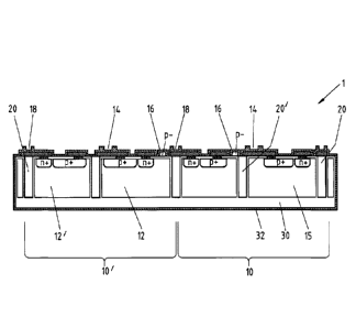
absorption in the substrate. Figure 2 shows a sectional side view of a portion
of an electrode
array 1, showing two adjacent pixels 10, 10'. The pixels 10, 10' correspond to
the pixels of
the pixel structure according to the embodiment as shown in Figure 1, having
two diodes 12,
10 12'. The same layer structure as shown in Figure 1 for a two-diode pixel
may essentially also
be provided for a one-diode or three-diode pixel, analogously.
Further, in Figure 2, a first material layer 30 is shown. That material layer
30 may be formed
as an integral part of the substrate 15, as in the case for the embodiment
shown in Figure 2.
15 Alternatively, the first material layer may at least partially be an
integral part of the substrate
15, or may be a layer deposited on the substrate 15.
The first material layer 30 is provided adjacent and subsequent to a back
surface of the
substrate 15. The first material layer 30 may, for instance, comprise a buried
oxide layer, in
particular an SiO2 layer. The buried oxide layer may be thermally grown on the
substrate 15.
The substrate layer preferably comprises silicon. In addition, the first
material layer 30 may
be a stacked layer comprising, subsequent to the buried oxide layer, a metal
layer, such as
an aluminium or titanium layer.
In the embodiment according to Figure 2, a second material layer 32 adjacent
to the first
material layer 30 is provided on a surface of the first material layer 30
which faces away from
the substrate 15. The second material layer 32 may comprise a metal, such as
aluminium or
titanium, or a stack of metals. Preferably, the outermost layer of the pixel
structure 10 at least
on the back surface of the substrate 15, i.e., the outermost layer of the
second material layer
32, comprises a material which allows a hermetic sealing of the back surface
of the substrate
15, or of the back surface of the substrate and at least a part of the side
portion of the pixel
structure. That way, as may be seen in Figure 2, the edge of the pixel
structure may be
hermetically sealed and the pixel structure may be protected from corrosion or
decay due to
environmental effects. In case that an entire pixel array 1, as shown in
Figure 3, or an implant
CA 02983617 2017-10-23
WO 2016/206809 PCT/EP2016/001073
16
shall be provided, the hermetic sealing may be provided on the outermost
layer, edge and/or
side portion of that pixel array 1.
It will be understood that the definition as a "layer", in particular with
respect to the first
.. material layer 30, is used in order to better describe the characteristics
of the pixel structure
10. However, as a consequence of the methods used to produce the pixel
structure 10
according to the invention, the individual layers such as the substrate 15,
the first material
layer 30 or the second material layer 32 may be integrated into another. The
Methods used
to provide the layer structure according to the present invention may for
instance include
thermal growing, ion deposition, electrochemical deposition, physical vapour
deposition,
such as sputtering and electron beam evaporation, or other methods.
Consequently, a pixel
structure produced accordingly may actually not appear to have a layer
appearance, or
display separable layers, while, functionally, layers, e.g. according to
embodiments of the
present invention, are in fact provided therein. According to a special
embodiment, at least
two "layers" can be separated by one adhesive layer 33. Said adhesive layer 33
may have a
thickness of preferably 5nm to 50nm, more preferably 10nnn to 30nm, most
preferred about
20nm +/- 5nm. The adhesive layer 33 may be formed of titanium which has good
adhesive
properties. Preferably, there is no adhesive layer 33 between layer 15 and 30
when the first
material layer 30 comprises buried oxide layer thermally grown on the
substrate 15.
Figure 3 shows an array of pixel structures 10, 10', i.e., a pixel array 1. In
the embodiment
shown in Figure 3, the pixel array 1 is an array of pixel structures 10, 10'
wherein each of the
pixel structures 10. 10' comprise a stimulating electrode 14 configured to
stimulate cells or
.. living tissue. Therefore, the pixel array 1 may also be referred to as an
electrode array. The
size of the individual pixel structures 10, 10' in the array 1 may differ and
can thus be tuned
to different applications, without departing from the scope of the present
invention. In the
array 1 displayed in Figure 3, the individual pixels 10, 10' are hexagonally
formed, which
allows a space efficient distribution on the substrate 15. That way, the space
available for
light sensitive regions on the substrate 15 and within an array 1 may be
increased and ideally
maximized. A pixel array 1 as shown in Figure 3 may for instance be used in an
implant in
order to stimulate cells or living tissue, in particular living tissue, such
as neural tissue, or
neural cells.
CA 02983617 2017-10-23
WO 2016/206809 PCT/EP2016/001073
17
According to embodiments of the present invention, not shown in Figure 3,
first and/or the
second material layer may be formed around the back surface of the array, i.e.
the surface
build by the plurality of back surfaces of the individual pixel structures. In
addition, the first
and/or second material layer may be formed around an edge of the array 1, in
order to provide
a sealing or protection to the array.
Figure 4 (a) shows a schematic cross section of a pixel array 1, which is
embedded in tissue,
here for instance in a retina 3. The pixel array 1 is represented by the
substrate 15, wherein
any surface structures, such as diodes or electrodes, are not displayed in the
figure.
Commonly, when implanting a pixel array 1, or an implant, into a retina 3, the
substrate is
arranged such that light, represented by the arrow 40 in Figure 4 (a), which
is incident on the
eye may traverse the retina and be incident on a front surface of the
substrate 15. From the
front surface of the substrate 15, the light enters and traverses the
substrate 15 where it is
absorbed depending on the material of the substrate 15, the wavelength of the
incident light,
and other factors. The substrate 15 used typically comprises or consists of
silicon.
For a typical thickness of 30pm of silicon substrate, and at a wavelength of
830nm of the
incident light, about 85% of the incident light is absorbed. At a wavelength
of 880nm, 68%
of the incident light are absorbed and at a wavelength of 915nm, only about
53% of the
incident light are absorbed. If the substrate is to be used in an implant in
order to restore
vision, the stimulation of a pixel structure 10 comprising the substrate 15
needs to be in the
infrared or near-infrared region of the spectrum, such that residual vision of
the retina is not
disturbed. The light, which is not absorbed in the substrate 15 is incident on
the back surface
of the substrate 15. At the back surface of the substrate 15, due to the
intrinsic material
properties and the laws of reflection, about 21% of the light is reflected
back into substrate
(not shown in Figure 4 (a)), while the bigger part of the light exits the
substrate 15 as indicated
with arrow 42 in Figure 4 (a) and is lost.
As displayed in Figure 4 (b), according to an embodiment of the present
invention, on the
back surface of the substrate 15 a first material layer 30 is provided
adjacent to the substrate
15. That first material layer 30 may also be a stack of materials. The first
material layer 30
comprises at least a reflective material layer, which increases the
reflectivity at the back
surface of the substrate. Thereby, an increased fraction of the light
initially transmitted through
CA 02983617 2017-10-23
WO 2016/206809 PCT/EP2016/001073
18
the substrate 15 without being absorbed may be reflected back into the
substrate 15, as
indicated with the arrow 41 in Figure 4 (b). Accordingly, less light will be
lost for a photo-
electrical reaction.
Figure 4 (c) displays a further embodiment of the present invention, according
to which a
second material layer 32 is provided adjacent to the first material layer 30.
Such a second
material layer 32 may allow a further increase in reflectivity at the back
surface of the substrate
15. That may further increase the absorption rate. The second material layer
32 may be a
material which allows a hermetic sealing, such as titanium. Thereby, the
reflectivity at the
back surface may be increased, while, at the same time, hermeticity of the
pixel structure 10
or the entire pixel array 1 or implant may be enabled. Further materials to
provide a hermetic
cover layer, coating or housing may be ceramic layers, such as aluminium
oxide, silicon
carbide or others.
Figure 4 (d) displays a further embodiment of the present invention, according
to which a
second material layer 32 is provided adjacent to the first material layer 30
similar to the
embodiment of Fig. 4 (c). Again, the second material layer 32 may allow a
further increase in
reflectivity at the back surface of the substrate 15. The first material layer
30 may be formed
of silicon dioxide, while the second material layer 32 may be formed of
Aluminium, having
.. a thickness of 100nm or more, or may be formed by a stack of Aluminium and
Titanium,
having a thickness of 100nm or more each. Between the second material layer 32
of
Aluminium, or Aluminium and Titanium, and the first material layer 30 of
silicon dioxide
there is arranged an adhesive layer 33 having a thickness of preferably 5nm to
50nm, more
preferably 10nm to 30nm, most preferred about 20nm +/- 5nm. The adhesive layer
33 may
be formed of titanium which has good adhesive properties.
Figure 5 shows a graph representing the reflection coefficient versus the
thickness of a buried
oxide layer of a stacked first material comprising the buried oxide layer and
an aluminium
layer (upper curve) and a buried oxide layer and a titanium layer (lower
curve). It will be
noted that the reflectivity of the BOX/Al-stack significantly surpasses that
of the BOX/Ti-stack
at and around a thickness of the buried oxide layer of 130nm, 430nm or 130nm
plus multiples
of 300nrn. Further, the slope of the curve of the BOX/Al-stack is flatter in
the range of that
preferred thicknesses of 130nm, 430nm or 130nnn plus multiples of 300nm of the
buried
oxide layer than the curve of the BOX/Ti-layer.
CA 02983617 2017-10-23
WO 2016/206809
PCT/EP2016/001073
19
The graphs displayed in Figure 5 are based on simulation results of a
substrate 15 consisting
of silicon, a first material layer 30 stacked of SiO2 and aluminium or
titanium, and a
subsequent retinal layer 3. Indices of refraction for that simulation were
assumed to be 3.66
for Si, 1.4525 for SiO2, 2.58 + 8.21 I for Al, 3.06 + 3.305 I for Ti, and 1.36
for the retinal
.
tissue at a wavelength of 880nm. While these data represent specific
embodiments of the
present invention, similar or same conclusions, in particular to the BOX-
thickness, may be
drawn also for different wavelength or material properties. These examples
shall not be
construed to limit the scope of the present invention to the specific
examples. Rather, various
implementations with different materials, material thicknesses, layer numbers,
reflective
indices and so on may be applied within the scope of the present invention.
It is further to be understood that according to the present invention, the
thickness of the BOX-
layer may be varied to thicknesses higher or lower than the indicated
preferred thickness of
around 130nm, 430nm or 130nm plus multiples of 300nm.