Note: Descriptions are shown in the official language in which they were submitted.
CA 02983882 2017-10-24
WO 2016/179437 PCT/US2016/031063
MULTI PROCESSOR PIPELINE ARCHITECTURE
CROSS-REFERENCE TO RELATED APPLICATIONS
[0001] This
application claims the benefit of priority to Provisional Patent Application
Serial No. 62/158,078 (01018100), filed May 7, 2015, entitled "Multiprocessor
Pipeline
Architecture"; and Provisional Patent Application Serial No. 62/260,995
(01018101), filed
November 30, 2015, entitled "Multiprocessor Pipeline Architecture", is related
to U.S. Patent
Numbers 8,467,061 and 8,649,011, both entitled "Integrated Analytical System
and
Method"; and to U.S. Provisional Patent Application Serial No. 62/042,793
(01018000), filed
August 27, 2014, entitled "Arrays of Integrated Analytical Devices and Methods
for
Production"; each assigned to the assignee of the present application, and
incorporated
herein will by reference.
BACKGROUND OF THE INVENTION
[0002]
Advances in biomolecule sequence determination, in particular with respect to
nucleic acid and protein samples, has revolutionized the fields of cellular
and molecular
biology. A sequencing instrument, such as a DNA sequencer, is used to automate
biomolecule sequence determination, e.g., a nucleic acid sequencing. Given a
sample of
DNA, a DNA sequencer is used to determine the composition of the biomolecule,
such as
the base composition of a nucleic acid molecule with respect to the order of
the four bases:
adenine, guanine, cytosine, and thymine. The order of the DNA bases is
reported as a text
string, called a read. Some DNA sequencers can be also considered optical
instruments as
1
SUBSTITUTE SHEET (RULE 26)
CA 02983882 2017-3.0-24
WO 2016/179437 PCT/US2016/031063
they analyze light signals originating from fluorochromes attached to
nucleotides. Third-
generation DNA sequencers such as SMRT and Oxford Nanopore measure the
addition of
nucleotides to a single DNA molecule in real time. Because of limitations in
DNA sequencer
technology these reads are short compared to the length of a genome therefore
the reads
must be assembled into longer contigs.
[0003] Typically, the final assembly of a genome is accomplished on other
computational resources off the sequencing instrument. Final assembly is
required on other
computational resources due to multiple reasons including the following: 1) a
need to
combine the results from multiple instrument runs or acquisitions (sometimes
from other
physical instruments), 2) the computational and memory resources required to
accomplish
the assembly are not available on the sequencing instrument, whether the
sequencer
instrument performs denovo shotgun assembly or an assembly aided by a
reference
sequence, 3) the use of third party assembler packages designed for running on
cluster
configurations, 4) assembly algorithms which are not designed to process data
as it streams
off the sequencing instrument, 5) assembly algorithms are designed to run on
conventional
computer architectures that are incapable of providing the computational
resources
necessary to perform assembly in real time.
[0004] What is desired is a sequencing system having a computational
architecture
that supports complete genome assembly from raw streaming data produced by a
sequencing instrument in real time, where the final result is the finished
genome sequence.
It is also desirable that the architecture is flexible and easily scalable to
increase the
throughput of the system, while at the same time reducing the costs associated
with the
2
SUBSTITUTE SHEET (RULE 26)
CA 02983882 2017-3.0-24
WO 2016/179437 PCT/US2016/031063
manufacturing and usage of the system.
BRIEF SUMMARY OF THE INVENTION
[0005] The exemplary embodiments are generally directed to multiprocessor
pipeline
architectures and methods that convert signals from sequencing sample
acquisition into
sequence data, comprising: a custom coprocessor card configured to directly
receive a
stream of serialized sensor data generated by an image sensor, wherein the
sensor data
represents frame-by-frame intensity values for pixels comprising the image
sensor, wherein
the image sensor captures images of light emitted from a plurality of reaction
cells of a
removable integrated sequencing chip; a first coprocessor that continually
receives the
stream of serialized sensor data and transposes the frame-by-frame intensity
values into
reaction cell chunks, each of the reaction cell chunks representing movie data
of the pixel
intensity values of a corresponding reaction cell across the frames over a
predetermined
time window; a buffer that repeatedly receives the reaction cell chunks and
stores in
contiguous memory locations the reaction cell chunks for each respective
reaction cell over
a larger predetermined time window to create larger reaction cell chunks; and
a plurality of
second coprocessors that retrieve the larger reaction cell chunks from the
buffer and
convert, in parallel, the pixel intensity values into base-by-base sequence
data even as
additional reaction cell chunks are received by the buffer, such that the
second coprocessors
begin raw base calling before all the sensor data for the sequencing sample
acquisition is
obtained.
3
SUBSTITUTE SHEET (RULE 26)
CA 02983882 2017-10-24
WO 2016/179437 PCT/US2016/031063
[0006] In yet another aspect, a multiprocessor pipeline architecture,
comprises: 1) a
sequencing instrument, comprising: a reservoir containing a solution
comprising a
sequencing reaction mixture including a sample to be sequenced and reagents
for carrying
out the nucleic acid sequencing reaction; an illumination source that provides
illumination; a
removable integrated sequencing chip in contact with the reservoir, the
integrated
sequencing chip comprising a plurality of analytical devices, each analytical
device
comprising a reaction cell, a waveguide, optical elements, and an image
sensor, wherein
the waveguide channels the illumination to the reaction cell, resulting in
emission of light
from the reaction cells that is passed by the optical elements to the image
sensor that detects
the light and converts the light into sensor data represented as frame-by-
frame intensity
values for each of the pixels comprising the image sensor, the sequencing chip
having a
coprocessor that serializes and outputs the stream of sensor data; and 2) a
primary analysis
server coupled to the sequencing instrument that converts the stream of sensor
data into
base calls, the primary analysis server comprising: a custom coprocessor
daughter card
configured to directly receive the stream of serialized sensor data over a
serial cable; at least
one coprocessor that transposes the frame-by-frame intensity values into
reaction cell
chunks, each representing movie data of the pixel intensity values of a
corresponding
reaction cell across the frames over a predetermined time window; a buffer
that repeatedly
receives reaction cell chunks and stores in contiguous memory locations the
reaction cell
chunks for each respective reaction cell over a larger predetermined time
window to create
larger reaction cell chunks; and wherein the at least one coprocessor
retrieves the larger
reaction cell chunks from the buffer and converts the pixel intensity values
into base-by-base
sequence data such that the conversion begins before all the sensor data for
the sequencing
4
SUBSTITUTE SHEET (RULE 26)
84106913
sample acquisition is obtained.
[0006a]
According to one aspect of the present invention, there is provided a
computer system comprising: a machine-readable medium, an image sensor
comprising a plurality of pixels, a primary analysis coprocessor card, a first
primary
analysis coprocessor having a plurality of I/O ports, a buffer, and a
plurality of second
processors, wherein the machine-readable medium encodes programming
instructions that comprise instructions for: obtaining from the image sensor,
as part of
a sequencing sample acquisition, a stream of serialized sensor data, wherein
the
serialized sensor data comprises frame-by-frame intensity values for the
plurality of
pixels of the image sensor representing optical measurements for sequencing
emitted from a plurality of reaction cells of a removable integrated
sequencing chip
over a plurality of frames, wherein each reaction cell in the plurality of
reaction cells
corresponds to a single molecular experiment; directly and continually
inputting the
stream of serialized sensor data at a rate of least 100 frames per second into
the
primary analysis coprocessor card; using the primary analysis coprocessor card
to
convert the stream of serialized sensor data into a format that can be input
directly
into the plurality of I/O ports of the first primary analysis coprocessor;
inputting the
formatted stream of serialized sensor data directly into the plurality of I/O
ports of the
first primary analysis coprocessor; using the first primary analysis
coprocessor to
transpose, in consecutive memory addresses, the frame-by-frame intensity
values of
the formatted stream of serialized sensor data into a corresponding plurality
of
reaction cell chunks, each reaction cell chunk in the corresponding plurality
of
reaction cell chunks representing movie data of the pixel intensity values of
a
corresponding reaction cell across the plurality of frames over a first
predetermined
time window; storing the corresponding plurality of reaction cell chunks in
contiguous
memory locations within the buffer over a second predetermined time window to
create larger reaction cell chunks; sending the larger reaction cell chunks
from the
buffer to the plurality of second processors; using, with at least some single
instruction multiple data (SIMD) instructions or multiple instruction multiple
data
(MIMD) instructions a plurality of logical cores of the plurality of second
processors to
Date Recue/Date Received 2021-04-30
84106913
convert, in each logical core in the plurality of logical cores, in parallel,
the pixel
intensity values into base-by-base sequence data concurrent with additional
reaction
cell chunks being received by the buffer from the first primary analysis
coprocessor,
causing the plurality of second processors to begin raw base calling before
all the
sensor data for the sequencing sample acquisition is obtained by the computer
system.
[0007] The invention and various specific aspects and embodiments will be
better understood with reference to the following detailed descriptions and
figures, in
which the invention is described in terms of various specific aspects and
embodiments. These are provided for purposes of clarity and should not be
taken to
limit the invention. The invention and aspects thereof may have applications
to a
variety of types of methods, devices, and systems not specifically disclosed
herein.
BRIEF DESCRIPTION OF SEVERAL VIEWS OF THE DRAWINGS
[0008] FIGS. 1A-1B are block diagrams showing hardware components the
multiprocessor pipeline architecture in accordance with exemplary embodiments.
[0009] FIG. 1C is a diagram showing a signal output for a real time
sequencing
operation using a two color/two amplitude signal set from set of two pixels
assigned
to the reaction cell_
[0010] FIG. 2 is a flow diagram illustrating multiprocessor pipeline
processing
that converts sensor data from nucleic acid sequencing into sequence data
according
to an exemplary embodiment.
[0011] FIG. 3 is a diagram illustrating a high-level view of the
subsystem
software components of the multiprocessor pipeline architecture.
[0012] FIG. 4 is a block diagram illustrating details of the hardware,
software
and interface modules of the primary analysis subsystem according to one
exemplary
embodiment.
5a
Date Recue/Date Received 2021-04-30
CA 02983882 2017-10-24
WO 2016/179437 PCT/US2016/031063
[0013] FIGS. 5A, 5B and 5C are block diagrams illustrating in further
detail the
processing performed by the primary analysis pipeline.
[0014] FIG. 6 is a diagram illustrating the processing performed secondary
analysis
pipeline in the secondary analysis server.
DETAILED DESCRIPTION OF THE INVENTION
[0015] Various embodiments and components of the present invention employ
signal
and data analysis techniques that are familiar in a number of technical
fields. For clarity of
description, details of known analysis techniques are not provided herein.
These techniques
are discussed in a number of available reference works, such as: R. B. Ash.
Real Analysis
and Probability. Academic Press, New York, 1972; D. T. Bertsekas and J. N.
Tsitsiklis.
Introduction to Probability. 2002; K. L. Chung. Markov Chains with Stationary
Transition
Probabilities, 1967; W. B. Davenport and W. L Root. An Introduction to the
Theory of
Random Signals and Noise. McGraw-Hill, New York, 1958; S. M. Kay, Fundamentals
of
Statistical Processing, Vols. 1-2, (Hardcover - 1998); Monsoon H. Hayes,
Statistical Digital
Signal Processing and Modeling, 1996; Introduction to Statistical Signal
Processing by R.M.
Gray and L.D. Davisson; Modern Spectral Estimation: Theory and
Application/Book and
Disk (Prentice-Hall Signal Processing Series) by Steven M. Kay (Hardcover -
Jan 1988);
Modern Spectral Estimation: Theory and Application by Steven M. Kay (Paperback
- Mar
1999); Spectral Analysis and Filter Theory in Applied Geophysics by Burkhard
Buttkus
(Hardcover - May 11, 2000); Spectral Analysis for Physical Applications by
Donald B.
Percival and Andrew T. Walden (Paperback - Jun 25, 1993); Astronomical Image
and Data
SUBSTITUTE SHEET (RULE 26)
CA 02983882 2017-10-24
WO 2016/179437 PCT/US2016/031063
Analysis (Astronomy and Astrophysics Library) by J. L. Starck and F. Murtagh
(Hardcover -
Sep 25, 2006); Spectral Techniques In Proteomics by Daniel S. Sem (Hardcover -
Mar 30,
2007); Exploration and Analysis of DNA Microarray and Protein Array Data
(Wiley Series in
Probability and Statistics) by Dhammika Amaratunga and Javier Cabrera
(Hardcover - Oct
21, 2003).
[00161 The exemplary embodiments provide a multiprocessor pipeline
architecture
capable of performing a complete genome assembly from raw streaming sensor
data
produced by sequencing instrument in real time with the final result of the
instrument being
the finished genome sequence, including per base quality values. The
multiprocessor
pipeline architecture is flexible and easily scalable to increase the
throughput of the system,
while at the same time reducing the costs associated with the manufacturing
and usage of
the system.
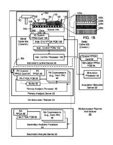
[00171 FIGS. 1A-1B are block diagrams showing hardware components the
multiprocessor pipeline architecture in accordance with exemplary embodiments.
In one
embodiment, the multiprocessor pipeline architecture 20 includes an instrument
control
server 24, which in turn includes a single molecule (e.g., nucleic acid)
sequencing instrument
100. The instrument control (IC) system 24 may also include an IC processor or
CPU 102
coupled to one or more IC printed circuit boards (PCBs) 104.
[00181 Other components of the instrument control (IC) system 24 include an
IC
coprocessor PCB 106 coupled to the IC PCBs 104, and an IC custom coprocessor
card 108
coupled to the IC coprocessor PCB 106. As is known in the art, the term
coprocessor refers
to a computer processor used to supplement the functions of a primary
processor (e.g., a
7
SUBSTITUTE SHEET (RULE 26)
CA 02983882 2017-10-24
WO 2016/179437 PCT/US2016/031063
CPU). As used herein, "coprocessor" may refer to a field programmable gate
array (FPGA),
an application-specific integrated circuit (ASIC), a graphics processing unit
(GPU), or any
combination thereof. FIG. lA shows an embodiment where certain coprocessors
are labeled
as FPGAs for clarity, but the exemplary embodiments are not to be limited to
this particular
embodiment.
[0019] SEQUENCING INSTRUMENT
[0020] The sequencing instrument 100 comprises a removable integrated
sequencing
chip 120 mounted in a socket 140. The sequencing chip 120 is generally
directed to optical
analyses of biological and/or chemical samples and reactions to provide for
the
simultaneous observation of multiple sequencing reactions in real time. In
general, these
optical analyses seek to gather and detect one or more optical signals, the
appearance or
disappearance of which, or localization of which, is indicative of a given
chemical or
biological reaction and/or the presence or absence of a given substance within
a sample
material. In some cases, the reactants, their products, or substance of
interest (all of which
are referred to as reactants herein) inherently present an optically
detectable signal which
can be detected. In other cases, reactants are provided with exogenous
labeling groups to
facilitate their detection. Useful labeling groups include fluorescent labels,
luminescent
labels, mass labels, light scattering labels, electrochemical labels (e.g.,
carrying large charge
groups), metal labels, and the like.
[0021] The sequencing instrument 100 may further include a reservoir 124
and an
illumination source 130, while the sequencing chip 120 may include one or more
couplers
121, routing waveguides 122, and an analysis region 123. The reservoir 124 is
in contact
8
SUBSTITUTE SHEET (RULE 26)
CA 02983882 2017-10-24
WO 2016/179437 PCT/US2016/031063
with the analysis region 123 and delivers to a solution 125 comprising a
sequencing reaction
mixture including a sample to be sequenced and reagents for carrying out the
nucleic acid
sequencing reaction. The reservoir 124 may be produced as part of the
packaging for the
analysis region 123
[0022] The illumination source 130 provides illumination in the form of one
or more
excitation light beams 132 to the sequencing chip 120. The illumination source
130 may
comprise, for example, a laser or group of lasers. The one or more light beams
132 from the
illumination source 130 are directed to one or more couplers 121 on the
sequencing chip
120. The couplers 121 couple the light beams 132 to the routing waveguides
122, which
propagate the light beams 132 to the analysis region 123 of the sequencing
chip 120.
[0023] FIG. 1B illustrates a not-to-scale close-up example of the analysis
region 123
of the sequencing chip 120. The analysis region 123 has an array of integrated
analytical
devices 123a for performing optical analysis, e.g., nucleic acid sequencing
processes, that
rely in part on non-spectral discrimination of differing signals, and
optionally, in part on
spectral distinction. The array of analytical devices 123a is useful, for
example, in the large-
scale sequencing of nucleic acids, including in particular, genomic
sequencing. The nucleic
acid sequencing can be single-molecule real-time nucleic acid sequencing.
[0024] The analysis region 123 may include anywhere from 1,000 to 100
million or
more analytical devices 123a. In one embodiment, however, the analysis region
123 may
include for example between 100,000 and 10 million, but preferably at least
500,000
analytical devices 123a. Such arrays can be produced by a variety of methods
(See for
example Pat. Application 01018000 entitled "Arrays of Integrated Analytical
Devices and
9
SUBSTITUTE SHEET (RULE 26)
CA 02983882 2017-10-24
WO 2016/179437 PCT/US2016/031063
Methods for Production," incorporated herein by reference).
[0025] While the components of each device and the configuration of the
analytical
devices 123a in the system may vary, each integrated analytical device 123a
typically
comprises, at least in part, the general structure described below. Each
analytical device
123a typically includes a reaction cell 123b. "Reaction cell" generally refers
to the location
where the reactants are disposed, the location where the reaction of interest
is occurring
and from which the optical signals emanate. In some cases, the reaction cell
123b will have
a biomolecule such as a polymerase enzyme immobilized within it, and a fluidic
conduit from
the reservoir 124 provides reagents across the reaction cells 123b. Thus, the
reaction cell
123b may hold an analyte (i.e., the polymerase-template complex and associated
fluorescent reactants) from which the optical signals emanate. In one
embodiment, the
reaction cell 123b comprises a nanowell or nanopore disposed in the surface
layer. Such
nanowells may constitute depressions in a substrate surface or apertures
disposed through
additional substrate layers to an underlying transparent substrate, e.g., as
used in zero mode
waveguide (ZMW) arrays (see, e.g., U.S. Patent Nos. 7,181,122 and 7,907,800).
In various
respects, "analytical device" refers to the reaction cell 123b and associated
components that
are functionally connected.
[0026] Below the reaction cell 123b is a routing waveguide 122a that
channels
excitation illumination to the reaction cell 123b from below, illuminating
reactants within the
reaction cell 123b. Use of optical waveguides to illuminate reaction cells is
described in e.g.,
U.S. Patent No. 7,820,983 and U.S. Patent Application Publication No.
2012/0085894,
which are each herein incorporated by reference. While a waveguide is shown
here, other
SUBSTITUTE SHEET (RULE 26)
CA 02983882 2017-10-24
WO 2016/179437 PCT/US2016/031063
optical elements such as those provided elsewhere herein can be used to
provide light from
under the reaction cell.
[0027] In some embodiments, excitation illumination results in the emission
of light
from the reaction cell 123b in order to allow for optical measurements of
sequencing. For
example, an analyte (e.g., a polymerase-template complex with associated
fluorescent
reactants) disposed within a reaction cell 123b emits fluorescent light. For
fluorescent
analytes, at least a portion of the analyte sample is illuminated by an
excitation light source,
whereas other analytes, such as chemilunimescent or other such analytes, may
not require
an excitation light source.
[0028] The optical elements 123d are optically coupled to a detector, such
as image
sensor 123e, and pass the light emitted from within the reaction cell 123b to
the image
sensor 123e. The optical elements 123d may include any combination of
apertures, lenses,
prisms, mirrors filters, beam shaping elements, refractive material, rejection
layers, and the
like, depending upon the application. The light emitted from the reaction cell
123b may be
further manipulated by the optical elements 123d, such as by diffractive beam
shaping
elements and color filtration layers, prior to reaching the image sensor 123e.
[0029] The emitted light passing through the optical elements 123d is
detected by the
image sensor 123e and converted into sensor data, comprising for example,
pixel intensity
values corresponding to optical signal pulses. Examples of the image sensor
123e may
include CCD (charge-coupled device) and CMOS (complementary metal-oxide
semiconductor) image sensors, both of which comprise an array of
pixels/photodiodes that
transform light into an electrical charge, the intensity of which is related
to a color in the color
11
SUBSTITUTE SHEET (RULE 26)
CA 02983882 2017-10-24
WO 2016/179437 PCT/US2016/031063
spectrum. In one embodiment, the image sensor 123e may comprise at least 2
megapixels.
[0030] The ability to distinguish different signal components may be
achieved through
the use of, e.g., different filtered optical elements, or the inclusion of
dispersive optical
elements to differentially direct different spectral components of a signal to
different pixels
or different regions of the image sensor. The light from a particular reaction
cell 123b is
directed to the image sensor 123e such that a set of n pixels of the image
sensor 123e is
assigned to detect the amplitude or intensity values for one reaction cell
123b. For example,
each reaction cell 123b could have one, two, three, four, or more pixels
assigned to detect
the intensity values emitted by the corresponding reaction cell 123b.
[0031] FIG. 1C is a diagram showing an exemplar signal output for a real
time
sequencing operation using a two color/two amplitude signal set from set of
two pixels
assigned to the reaction cell 123b over time (i.e., a time-series, where one
trace (dashed)
denotes signals associated with incorporation of A (high intensity signal) and
T (lower
intensity signal) bases, while the other signal trace (solid line), denotes
the signals of a
different emission spectrum, associated with G (high) and C (low) bases. The
timing of
incorporation and the identity of the base incorporated, as derived from the
color channel
and intensity of the signal, are then used to interpret the base sequence.
[0032] The exemplary system of FIG. 1A is configured for genomic
sequencing. In
operation generally, a sample from the reservoir 124 is delivered to
analytical devices 123a
for data collection. The instrument control processor 102, which is in
communication with
the sequencing chip 100, sets up data acquisition and instructs the image
sensor 123e when
to start capturing images. In response, the image sensor 123e may generate and
output
12
SUBSTITUTE SHEET (RULE 26)
CA 02983882 2017-10-24
WO 2016/179437 PCT/US2016/031063
analog sensor data representing raw pixel data. In one embodiment, the analog
sensor data
may be a serialized 16 or 32 bit interface, with 11 bits per pixel. In one
embodiment, the
sensor data may be output at 100 frames per second, and include approximately
2 million
pixels per frame. Thus, sensor data as a whole may represent frame-by-frame
intensity
values for the pixels comprising an image sensor 123e.
[00331 The sequencing chip 100 outputs the stream of sensor data from the
image
sensor 123e through contacts 129 on the sequencing chip 100, which may mate
with
contacts 142 on the socket 140. In one embodiment, the contacts 129 may
comprise ball
contacts, however other types of contacts may be used. In one embodiment, the
socket 140
sends unmodified sensor data. In an alternative embodiment, the socket 140 may
have
electronics, such as a coprocessor (not shown), for altering the electrical
trace signals before
transmission to the primary analysis server 26.
[00341 In one embodiment, the analysis region 123 may be configured for
single use
as a consumable, and as such, discarded after sample acquisition and replaced
with a new
analysis region 123. Some sequencing experiments may require the use of
multiple analysis
region 123.
[0035] Although the sequencing chip 100 represents a technological
advancement,
conventional computational architectures are incapable of executing primary
analysis and
consensus base calling in real-time using the output of the sequencing chip
100. For
example, the sensor data must be input into the computational architecture at
a throughput
too fast for conventional processors to even store the data to disk. In
addition, to sequence
the 3 billion base human genome where 30X coverage is needed to guarantee
sufficient
13
SUBSTITUTE SHEET (RULE 26)
CA 02983882 2017-10-24
WO 2016/179437 PCT/US2016/031063
quality of the result, approximately 12 analysis regions 123 and corresponding
acquisition
processes may be required depending on the number of reaction cells 123b
present in the
analysis region 123. The amount of data produced during these multiple
acquisition
processes would require an amount of memory for storage and processing that
would
exceed the capacity of typical processor boards.
[00361 MULTIPROCESSOR PIPELINE ARCHITECTURE
[00371 The exemplary embodiments overcome the throughput and memory issues
of
conventional computational architectures presented by the sequencing chip 100
by
providing a multiprocessor pipeline architecture that performs primary
analysis through
consensus base calling in substantially real-time. The multiprocessor pipeline
architecture
is designed to provide necessary parallelized computational resources and
memory
bandwidth needed to perform the entire genome assembly in "chunked" real time,
as
explained below. The overall system architecture has a modular design such
that system
can be scaled efficiently by adding or subtracting components, and therefore
scales in cost
depending on the size of the genome being sequenced.
[00381 Referring again to FIGS. 1A and 1B, details regarding the hardware
aspects
of the multiprocessor pipeline architecture will be described. According to
the exemplary
embodiment, the pipeline architecture has several subsystems, including the
instrument
control server 24, a primary analysis server 26, a secondary analysis server
28, and an
optional acquisition simulator server 30. In one embodiment, the instrument
control server
24 and the primary analysis server 26 may be housed in close proximity within
an on-
instrument platform 22. The acquisition simulator server 30 may communicate
with the
14
SUBSTITUTE SHEET (RULE 26)
CA 02983882 2017-10-24
WO 2016/179437 PCT/US2016/031063
instrument control server 24, and the primary analysis server 26 may
communicate with both
the instrument control server 24 and the secondary analysis server 28.
[0039] The IC custom coprocessor card 108 in the instrument control system
102
receives the analog stream of raw pixel data output from the socket 140 of the
sequencing
instrument 100 and converts the analog stream of raw pixel data into a
serialized bitstream
of sensor data. In one embodiment, the sensor data is digitized and the data
encoding may
be modified to 8 bit or 10 bit to minimize errors. The format of the bitstream
includes headers
and data packets that form a complete image frame that will be reconstructed.
Thus, the
sensor data output by the IC custom coprocessor card 108 represents frame-by-
frame
intensities for each of the pixels of the image sensor 123e. The serialized
bitstream of sensor
data is output to the primary analysis server 26 for analysis and further
processing.
[0040] The primary analysis server 26 carries out analysis to convert raw
pixel data
to base calls, after which, this data may be transferred off the on-instrument
platform 22 and
to the secondary analysis server 28 for secondary analysis, such as assembly.
In another
embodiment, if the primary analysis server 26 is provided with sufficient
computational
resources, then secondary analysis processing could also be performed within
the primary
analysis server 26.
[0041] In one embodiment, primary analysis server 26 comprises a primary
analysis
(PA) processor 42, a plurality of PA coprocessors 40, and a PA custom
coprocessor card
34 and PA coprocessor 36 coupled to a PA coprocessor PCB 38. In one
embodiment, the
primary analysis server 26 may be on-instrument, as shown. In a second
embodiment, the
primary analysis server 26 may be located on-chip as part of the socket 140.
And in a third
SUBSTITUTE SHEET (RULE 26)
CA 02983882 2017-3.0-24
WO 2016/179437 PCT/US2016/031063
embodiment the primary analysis server 26 may be located on a remote computer.
[0042] The secondary analysis server 44 carries out analysis to produce
consensus
base calling and assembly data. The architecture of the secondary analysis
server 28 may
be similar to that of the primary analysis server 26. In one embodiment, the
secondary
analysis server 26 comprises a secondary analysis (SA) processor 44, a
plurality of SA
coprocessors 46, and a SA coprocessor 40 coupled to a SA coprocessor PCB 50.
[0043] The acquisition simulator server 30 may be used to interface with
the
instrument control server 24. The acquisition simulation server 30 may
comprise a simulation
processor 52, and a simulation custom coprocessor card 56 coupled to a
simulation
coprocessor PCB 54. In one embodiment the acquisition simulator server 30 may
transmit
simulated sensor data to the instrument control server 24 to enable the
instrument control
server 24 to input simulated signal data/frames to the primary analysis server
26 via serial
cable 32b without the need for the sequencing instrument 100. In a further
embodiment, the
acquisition simulator server 30 can also be connected directly to the PA
custom FPGA card
34 in the primary analysis server 26 to input simulated signal data/frames via
serial cable
32c without the need of the instrument control server 24.
[0044] In one exemplary embodiment, the PA coprocessor 36 and SA
coprocessor
48 may comprise an FPGA or an ASIC, while the PA coprocessors 40 and SA
coprocessors
46 may comprise an Intel Many Integrated Core Architecture coprocessor (i.e.,
Xeon PhiTM)
or the like. In an alternative embodiment, a combination FPGA and Xeon Phi
coprocessors
(or the like) could be used. In one exemplary embodiment, the use of FPGAs is
preferred
because FPGAs may aid in reducing the size and cost of the system during
development.
16
SUBSTITUTE SHEET (RULE 26)
CA 02983882 2017-3.0-24
WO 2016/179437 PCT/US2016/031063
Once the system is configured in FPGA logic, ASICs may be created in place of
the FPGAs.
As an alternative to the Xeon Phi cards, GPU technology could be used.
However, Xeon Phi
cards present an advantage in terms of development environment.
[0045] Additionally, the PA processor 42, the SA processor 44, and the
simulation
processor 52 are coupled to respective memory, input/output (I/O), and network
interface
cards via a system bus or buses (not shown).
[0046] FIG. 2 is a flow diagram illustrating multiprocessor pipeline
processing that
converts sensor data from sequencing sample acquisition into sequence data
according to
an exemplary embodiment. The process may begin by the PA custom coprocessor
card 34
directly receiving the serialized sensor data generated by the image sensor
(block 200).
[0047] According to one aspect of the exemplary embodiment, the PA custom
coprocessor card 34 and the IC custom coprocessor card 108 are customized by
configuring
the cards 34, 108 with cable connectors that mate with the serial cable 32a,
which transfers
the sensor data. Likewise, the custom coprocessor card 56 in the acquisition
simulator
server 30 is customized by configuring the card 56 with a cable connector that
mates with
respective serial cables 32a, 32b and 32c.
[0048] In one embodiment, the serial cables 32a, 32b and 32c comprise high
speed
cables, such a coaxial cable, a twisted pair copper wire, an optical fiber,
and the like. In an
alternative embodiment where the subsystems are separated over large
distances, the serial
cables 32a, 32b and 32c may optionally comprise will Ethernet cables. If
needed, the custom
FPGA cards 128, 56, and 34 could be configured with more than one connection
and
accompanied logic if needed.
17
SUBSTITUTE SHEET (RULE 26)
CA 02983882 2017-3.0-24
WO 2016/179437 PCT/US2016/031063
[0049] In one embodiment, the PA custom coprocessor card 34 and the PA
coprocessor 36 are connected to the PA coprocessor PCB 38 via respective bus
connectors.
The PA custom coprocessor card 34 has wire connectors extending to the bus
connector of
the PA coprocessor PCB 38. In operation, the PA custom coprocessor card 34
receives the
serialized bitstream of sensor data over the serial cable 32a from the IC
custom coprocessor
card 108 and converts the data into a format that can be input directly into
the I/O ports of
the PA coprocessor 36 via the connectors to the PA coprocessor PCB 38 that
route the
serial data to the correct pins of the PA coprocessor 36. In one embodiment
the PA
coprocessor PCB 38 may comprises a PCIe card and includes an edge connector
designed
to plug-in into a PCIe bus of the PA coprocessor PCB 38 motherboard (not
shown). In an
alternative embodiment, the primary analysis server 26 may be provided with a
plurality of
PA custom FPGA cards 34 if needed to satisfy a higher multiplex of reaction
cells/ZMWs
123b data being output from the instrument control server 24. In other words,
there could
be multiple serial cables 32 a connecting the instrument control server 24 to
multiple PA
custom FPGA cards 34 (or multiple cables input into a single PA custom FPGA
card 34)
depending on the serial transmission bandwidth limits and the processing
limits of the
FPGAs themselves.
[0050] The IC custom coprocessor card 108 the PA custom coprocessor card
34, and
the custom coprocessor card 56 may include the same type of transceiver
receiver chipset
for digital communication. In the case of the PA custom coprocessor card 34,
the transceiver
chipset routes the data to traces on the PA coprocessor PCB 38, which then
sends to data
to the correct connector location hooked up to the PA coprocessor 36. In the
embodiment
where the serial cable 32a is a coaxial cable, the protocol governing the
transmission of the
18
SUBSTITUTE SHEET (RULE 26)
CA 02983882 2017-3.0-24
WO 2016/179437 PCT/US2016/031063
data of the serial cable 32a may comprise an Aurora protocol, which is a
Xilinx designed
transmission protocol. For example, the PA custom coprocessor card 34 may use
Aurora IP
logic to transfer the digital data over the coaxial cable. However, other
transmission
protocols may also be used.
[0051] Through the use of the chipset, both the IC custom coprocessor card
108 and
the PA custom coprocessor card 34 are capable of both sending and receiving
digital data.
According to another aspect of the exemplary embodiment, this enables the
acquisition
simulator server 30 to input simulation data/frames from the custom
coprocessor card 56
and a serial cable 32b to the instrument control coprocessor PCB 106. The
simulation
data/frames are then passed through to the IC custom coprocessor card 108 and
on to the
PA custom coprocessor card 34. Running simulation data/frames to the
multiprocessor
pipeline allows operators to verify that the instrument control server 24 and
primary analysis
server 26 are operating properly.
[0052] Unlike conventional PCIe FPGA cards, the sensor data is being input
directly
into the PA custom coprocessor card 34 and the PA coprocessor 36 without first
being input
into the PA processor 42 or other computer and then passing the data to an
FPGA. This is
in contrast to conventional coprocessor cards in which image data is first
input to a CPU and
then passed to the FPGA, and requires the use of a frame grabber. The
disadvantage of
first going through a CPU is that it requires the use of a frame grabber board
to take image
data, which saps the processing power of the CPU just to input the data into
the CPU and
increases the cost of the system due to the cost involved with the need for
additional CPU
power to perform data processing on the same CPU.
19
SUBSTITUTE SHEET (RULE 26)
CA 02983882 2017-3.0-24
WO 2016/179437 PCT/US2016/031063
[0053] In one exemplary embodiment, the PA custom coprocessor card 34 may
comprise a customized version of a commercially available Conway FPGA
Wolverine card.
The PA coprocessor 36 and the SA coprocessor 48 may, for example, comprise a
commercially available Xilinx Vertex FPGA, while the PA coprocessors 40 and
the SA
coprocessors 46 may comprise Intel Xeon Phi cards.
[0054] As stated above, the sensor data represents frame-by-frame intensity
values
for pixels comprising the image sensor, where a set of n pixels of the image
sensor 123e is
assigned to detect the intensity values emitted by each of the reaction cells
123b.
[0055] Referring again to FIG. 2, the PA custom coprocessor 36 continually
receives
the stream of serialized sensor data and transposes the frame-by-frame
intensity values into
reaction cell chunks, each representing movie data of the pixel intensity
values of a
corresponding reaction cell across the frames over a predetermined time window
(Block
202).
[0056] In one embodiment, the reaction cell chunks (also referred to as
chunked data
sets) each represent movie data of the intensity values of the set of pixels
assigned to a
corresponding reaction cell across the frames. In an exemplary embodiment, the
intensity
values of the pixels for each of the reaction cell chunks are stored in
contiguous memory
locations.
[0057] The buffer 39 repeatedly receives reaction cell chunks and stores in
contiguous memory locations the reaction cell chunks for each respective
reaction cell over
a larger predetermined time window to create larger reaction cell chunks,
referred to herein
as super reaction cell chunks (block 204).
SUBSTITUTE SHEET (RULE 26)
CA 02983882 2017-10-24
WO 2016/179437 PCT/US2016/031063
[0058] The PA coprocessors 40 retrieve the larger reaction cell chunks from
the buffer
and convert, in parallel, the pixel intensity values into base-by-base
sequence data even as
additional reaction cell chunks are received by the buffer, such that the PA
coprocessors 40
begin raw base calling before all the sensor data for the sequencing sample
acquisition is
obtained (block 206).
[0059] According to the exemplary embodiment, the PA coprocessor 36 (e.g.,
FPGA)
transposes the frame-by-frame intensity values into the reaction cell chunks,
while the PA
coprocessors will (e.g., Xeon Phi chips) perform the base calling. However, as
hardware
designs continually improve, both processes may be performed by a single
coprocessor
(e.g., an FPGA/ASIC) or by multiple ones of the same type of coprocessors
(e.g., all
FPGA/ASICs or all Xeon Phi chips).
[0060] FIG. 3 is a diagram illustrating a high-level view of the subsystem
software
components of the multiprocessor pipeline architecture, where like reference
numerals
shown in FIGS. 1A have like components. As described above, the on-instrument
platform
22 may include instrument control server 24 and the primary analysis server
26, while an
off-instrument platform 60 may include a secondary analysis server 28 and/or a
tertiary
analysis server 62. Both the on-instrument platform 22 and the off-instrument
platform 60
may be controlled by the remote computer 30', which is also off-instrument.
[0061] An instrument control subsystem 24a of the instrument control server
24
comprises instrument software modules 24b, common modules 24c and a web
interface
24d. A primary analysis subsystem 26a in the primary analysis server 26
comprises primary
software modules 26b, common modules 26c, and a web interface 26d. A secondary
21
SUBSTITUTE SHEET (RULE 26)
CA 02983882 2017-3.0-24
WO 2016/179437 PCT/US2016/031063
analysis subsystem 28a in the secondary analysis server 28 comprises secondary
software
modules 28b, common modules 28c, application workflows 28e, and a web
interface 28d. A
tertiary analysis subsystem 62a of the tertiary analysis server 62 comprises
tertiary software
modules 62b, common modules 62c and a web interface 62d.
[0062] Functions of the instrument software modules 24b of the instrument
control
server 24a include instrument control routines for robot and environmental
settings for the
sequencing instrument 100. For example, the instrument control modules 24b
communicates with the image sensor 123e and controls the transfer of the
sensor data from
the sequencing chip 120 to the IC custom coprocessor card 108. The instrument
control also
handles illumination source 130 control, robotic control for sample
preparation, and
environmental control for maintaining temperatures within the system.
Instrument control
settings or parameters of the instrument software modules 24b may be
configured by the
user interface 64a on the remote computer 30'. In one embodiment, the
instrument software
modules 24b may execute on the instrument control processor 102.
[0063] The primary software modules 26b refer to the primary analysis
pipeline
modules in the primary analysis server 26 that convert raw pixel data into
base calls. The
primary software modules 26b are described in further detail with respect to
FIG. 4.
[0064] The secondary software modules 28b refer to secondary analysis
pipeline
modules in the secondary analysis server 28 that may include alignment,
consensus calling
and pre-assembly modules, to generate an assembled genome.
[0065] The tertiary analysis server 62 and tertiary software modules 62b
may refer to
any additional third-party supplied hardware and software that may be used for
additional
22
SUBSTITUTE SHEET (RULE 26)
CA 02983882 2017-10-24
WO 2016/179437 PCT/US2016/031063
analysis of the data. The common modules 24c, 26c, 28c, and 62c handle data
management
for any disk drives and health monitoring of common components, such as the
disk drives
that are required by all subsystems. In one embodiment, the common modules
24c, 26c,
28c, and 62c may execute on the processors associated with the respective
subsystems.
[00661 To provide high degree of system-wide reliability, each of the
subsystems 24a,
26a, 28a, and 62a may include multiple software and hardware components to
monitor and
manage subsystem's health. Required hardware initialization and startup of
subsystem
processes may be defined in subsystem-specific configuration files, and
executed at node
startup by a subsystem watchdog daemon process. Once subsystem initialization
completes, the watchdog process enters in subsystem monitor mode. The watchdog
process constantly queries the status of configured subsystem processes,
coprocessors and
other hardware components, and when the watchdog process detects an anomaly,
such as
missing or unresponsive process, the watchdog process may attempt to correct
the problem,
i.e. restarting processes accordingly with their configuration. If the problem
cannot be
corrected, the watchdog process may restart the entire node, or perform
additional
diagnostics. Each of the subsystems 24a, 26a, 28a, and 62a may also include
finer
granularity health management services using a dedicated server component.
This
component may collect and store statistics at node level, from operating
system and
subsystem processes and services. Metrics collected and analyzed may trigger
policy based
actions, such as free-disk-space-threshold file delete/archive, or message-
level-based user
interface warning/alarm.
[0067] According to one aspect of the exemplary embodiment, each of the
23
SUBSTITUTE SHEET (RULE 26)
CA 02983882 2017-10-24
WO 2016/179437 PCT/US2016/031063
subsystems 24a, 26a, 28a, and 62a is provided with respective web interfaces
24a, 26a,
28a, and 62a that make the subsystems appear as a website and make the
subsystems
remotely accessible by the user interface 64a. The remote computer 30'
includes a user
interface 64a, which may be based on a client browser 64b, and a web interface
64d for
controlling each of the subsystems 24a, 26a, 28a, and 62a over a network.
[0068] According to the exemplary embodiment, one added benefit of the
multiprocessor pipeline scheme is that the use of remote computer user
interface 64d and
the respective web interfaces may enable different software modules 24b, 26b,
28b, and
62b, including the common modules 24c, 26c, 28c, and 62c and application
workflows 28e,
to be downloaded and/or updated. For example, a different PA custom FPGA
pipeline 422
could be downloaded to the PA custom FPGA card 34' before the sequencing
begins. The
PA custom FPGA card 34' could also be reloaded "on-the-fly" with additional
pipeline logic,
if necessary, while intermediate results are maintained in memory during the
chunk
processing. This enables a single physical FPGA to serve as multiple pipeline
steps if the
total processing time allows.
[0069] Also, in the same way that the primary analysis pipeline modules can
be
switched, a different secondary analysis pipeline could be downloaded to the
secondary
analysis server 20 based on the genome size, and whether a mapped assembly
(human or
other known genome) or denovo assembly is to be performed. Reference genomes
can be
stored in non-volatile memory on the secondary analysis server 20 and updated
via a
wireless connection. The ability to change the secondary analysis pipeline
quickly (possibly
within 100 ms) enables other types of processing for specific applications
beyond assembly.
24
SUBSTITUTE SHEET (RULE 26)
CA 02983882 2017-3.0-24
WO 2016/179437 PCT/US2016/031063
For example, the tertiary analysis server 62 may be provided with different
downloadable
"instrument application modules" for further post processing of the assembled
genome.
From a business perspective, the instrument control server 24, the primary
analysis server
26, the secondary analysis server 28, and the tertiary analysis server 62 may
be configured
with specific applications and may be even priced based on those applications,
while from
an engineering perspective the same underlying multiprocessor pipeline
architecture is
utilized.
[0070] In a further embodiment, the web interfaces 24d, 26d 28d, 62d and
64d may
be used to enable exchange of data using shared file systems and network
communication
protocols. Data availability, integrity and management are relevant and
challenging, given
current technologies limitations and expected average data produced and
exchanged of
many terabytes per day per instrument and analysis subsystems. To help provide
best
access performance, facilitate deployment, storage virtualization, integrity
preservation, and
extensible analytics and management functions, all user generated data and
metadata may
be stored in a different location from the core operating system, software
modules and
common modules. Results from acquisitions, primary analysis, secondary
analysis, user
protocols and more, may be organized in multiple directory structures, or
branches,
connected to the root of a virtual subsystem repository. Each block of
resources associated
with a particular entity, or store, may include metadata about content
categories, service
policies, list of resources, checksums, audit trail and so forth,
[0071] The software and common modules may connect to a repository by
linking to
the shared filesystem and communicating using the web interfaces. Transfer
services
SUBSTITUTE SHEET (RULE 26)
CA 02983882 2017-3.0-24
WO 2016/179437 PCT/US2016/031063
provide high performance bi-directional transfer to/from filesystem, http/ftp
servers, i.e.
cloud, and repository-to-repository. Data management services may monitor the
repository
and apply user defined policies, e.g. aging based deletion/archival. Other
services may be
provided by external components, such as advanced search analytics.
[0072] In one embodiment, the remote computer 30' may be the same computer
as
the acquisition simulator server 30 of FIG. 1A, and may be an optional part of
the system
that is provided by a third party. In one embodiment, the acquisition
simulator/remote
computer 30' is capable of inputting simulated sensor data into the
multiprocessor pipeline
system for analysis via the serial cable (e.g. coaxial cable) 32b. This
enables the
multiprocessor pipeline system to process either real data or simulated data
at the same
frame rate produced by the sensor chip 120.
[0073] FIG. 4 is a block diagram illustrating details of the hardware,
software and
interface modules of the primary analysis subsystem 26a (FIG. 3) according to
one
exemplary embodiment. The primary analysis computer 42 includes the web
interface 26d,
global shared memory blocks shown as a super chunk buffer 400 and an annotated
HQ
base calls buffer 402, and a post primary pipeline 404. Oval shapes in FIG. 4
denote
software modules executing in the primary analysis computer 42, the PA FPGA
36' and the
PA Xeon Phi cards 40'.
[0074] The web interface 26d includes a PA web client 406 and a PA web
server 408.
The PA web client 406 communicates with the PA processor to/from the
instrument control
server (ISC) processor interface 410, and sends outgoing inter-
process communication (IPC) messages 412 from executing processes. The PA web
server
26
SUBSTITUTE SHEET (RULE 26)
CA 02983882 2017-10-24
WO 2016/179437 PCT/US2016/031063
408 communicates with the ICS CPU to/from PA CPU Interface 414 and the PA Ul
to/from
PA CPU Interface 416, receives incoming IPC messages 418.
[0075] The PA FPGA card 36' and the PA Xeon Phi cards 40' connect to PCIe
slots
in the PA processor motherboard (not shown). In one embodiment, the PA
processor 42
may comprise a conventional multicore CPU having, for example, 24 cores, 512
GB of RAM,
and four PCIe slots.
[0076] The PA custom FPGA card 34' is shown customized with a
serial/coaxial cable
connector 420 that connects the coaxial cable 32a' to the PA custom FPGA card
34'.
According to one aspect of the exemplary embodiment, the serialized sensor
data received
via the coaxial cable 32a' flows through a real time primary analysis pipeline
comprising a
PA custom FPGA pipeline 422 executing in the PA FPGA 36', the super chunk
buffer 400,
a PA Phi pipeline 432 executing on the PA Xeon Phi cards 40', the annotated HQ
base calls
buffer 402, and a post primary pipeline 404 executing on the PA processor 42.
[00771 The PA custom FPGA pipeline 422 converts the pixel intensities in
the
serialized sensor data into reaction cell (e.g., ZMW) chunks representing
movie data
showing the pixel intensity values (i.e., trace signals) emitted by the
respective ZMWs over
time. The reaction cell chunks, which also may be referred to as ZMW movie
data, are
streamed out of the PA FPGA card 36' through a PA FPGA to/from PA CPU
interface 428
and stored in the super chunk buffer 400 for creation of the super reaction
cell chunks.
Output and buffering of the super reaction cell chunks/ZMW movie data is
controlled by a
PA CPU acquisition module 430 executing on the PA processor 42, which may
utilize direct
memory access (DMA).
27
SUBSTITUTE SHEET (RULE 26)
CA 02983882 2017-10-24
WO 2016/179437 PCT/US2016/031063
[0078] A PA CPU pipeline module 438 executing on the PA processor 42
coordinates
the transfer of the super reaction cell chunks from the super chunked buffer
400 to the PA
Phi pipelines 432 executing on the PA Xeon Phi cards 40'. The reaction cell
chunks pass
through a PA CPU to PA Phi interface 434 on the way to the PA Xeon Phi cards
40'.
[0079] The PA Phi pipeline 432 performs stream processing that converts the
super
reaction cell chunks/ZMW movie data into annotated high-quality (HQ) base
calls, which are
stored in annotated HQ base calls buffer 402 by the PA CPU pipeline 438. In
one
embodiment, for example, there may be 120 copies of the PA Phi pipeline 432
running
simultaneously on each of the PA Xeon Phi cards 40'. The annotated HQ base
calls are
stored in annotated HQ base calls buffer 402 until all the sensor data from
sample acquisition
for one super reaction cell chunk delta of time has been processed. The entire
pipeline
processing up to this point occurs in real time at least at 100 frames per
second or 450 MB
per second of incoming pixel data. In one embodiment, the PA CPU acquisition
module 430
and the PA CPU pipeline module 438 may be implemented as the same
multithreaded
component.
[0080] In one embodiment, both the super chunk buffer 400 and annotated HQ
base
calls buffer 402 are implemented as a portion of the memory of the PA
processor 42 that is
set aside as a temporary holding place for data shared by modules that operate
at different
speeds or with different sets of priorities.
[0081] Once all the annotated HQ base calls for one super reaction cell
chunk time
window have been created and stored, the raw base file write process 440
writes the data
to disk as a raw base file 442, which is in a customized format. In one
embodiment, the raw
28
SUBSTITUTE SHEET (RULE 26)
CA 02983882 2017-10-24
WO 2016/179437 PCT/US2016/031063
base file 442 may be stored in a proprietary format that is designed for the
efficiency for the
writing of data as fast as possible.
[0082] Once the raw base file 442 is closed, the file is processed by the
post primary
pipeline 404 executing on the PA processor 42. The post primary pipeline 42
comprises
software modules that operate on the raw base file 442 to create a standard
format
annotated HQ raw base file 458. During with the execution of the post primary
pipeline 42
another sample acquisition begins that is processed by the real-time primary
analysis
pipeline for creation of a new raw base file, while the current raw base file
442 is processed
during post processing.
[0083] The software modules may include any of an HQ, RQ score & statistics
generation module 444, a read quality filtering module 446, an adapter spike-
in-control
annotation module 448, a barcode data separation module 450, and a standard
file format
generation module 452 and a PA CPU base file transfer module 456. The
annotated high-
quality raw base calls generated by the post primary pipeline 404 are written
out by the
standard file format generation module 452 as an industry standard format file
454. The PA
CPU base file transfer module 456 executing on the PA processor 42 completes
the process
by writing the annotated HQ raw base file 458 to disk. The completed annotated
HQ raw
base file 458 may be then output from the PA analysis server 26 to the
secondary analysis
server 28 for secondary base processing.
[0084] FIGS. 5A, 5B and 5C are block diagrams illustrating in further
detail the
processing performed by the primary analysis pipeline 500. Oval shapes in
FIGS. 5A, 5B
and 5C denote executing software modules, square shapes represent data, and
squares
29
SUBSTITUTE SHEET (RULE 26)
CA 02983882 2017-3.0-24
WO 2016/179437 PCT/US2016/031063
with rounded corners represent files and messages.
[0085] According to one embodiment, the primary analysis pipeline 500
includes the
PA custom FPGA pipeline 422 executing on the PA FPGA Card 36', the PA Phi
pipeline 432
executing on the PA Xenon Phi cards 40', and the post primary pipeline 404
executing on
the PA processor 42.
[0086] PA CUSTOM FPGA PIPELINE PROCESSING
[0087] Referring to FIG. 5A, processing begins with the PA Custom FPGA
Pipeline
422, which may include a dark/screen frame correction module 502, a cross talk
mitigation
module 504, a transpose module 506 and a write to buffer module 508. The PA
Custom
FPGA Pipeline 422 receives the sensor data from the sequencing instrument 100
as frames
of raw pixel data 501. In one embodiment, 100 frames/sec are received where
each frame
comprises approximately 2 million pixels at 12 bits per/pixel.
[0088] The first step is for the dark frame and gain correction module 502
to perform
dark frame and gain correction. Because the sequencing chip 120 includes an
integrated
image sensor 123e and is disposable after each sample acquisition, the image
sensor 123e
of each sequencing chip 120 has slightly different characteristics. Therefore,
prior to
receiving the stream of sensor data, the dark frame and gain correction module
502 first
performs an image sensor calibration to determine pixel values for a dark
frame output by
the image sensor in absence of any input lighting. That dark frame is then
subtracted from
all input frames. The dark frame and gain correction module 502 also performs
a gain to
remove any gain applied to the frames during image capture.
[0089] Once the dark frame and gain correction module is performed, the
cross talk
SUBSTITUTE SHEET (RULE 26)
CA 02983882 2017-3.0-24
WO 2016/179437 PCT/US2016/031063
mitigation module 504 performs cross talk mitigation to mitigate any
electronic bleed of light
between pixels produced by the image sensor 123e by subtracting any such
bleeding light
from the pixels. In one embodiment, the cross talk mitigation may utilize at
least one of
generalized least squares and first or second-order inverse approximation.
[0090] The dark frame and gain correction and cross talk mitigation occur
in real time
on the PA custom FPGA card 34'. The result is corrected pixel data 510 at a
rate of 100
frames per second. As a more specific example, the corrected pixel data 510
comprise 2.07
MP frames output at 100 fps, 16 bits/pixel (415 Mbytes/sec).
[0091] The corrected pixel data 510 is then processed by the transpose
module 506.
The raw pixel data 500 is originally input such that the frames are stored in
consecutive
memory addresses in pixel order, which is spatially based (The light emitted
by each reaction
cell/ZMW 123b is represented by the same set of pixels (e.g. 2 pixels) in each
frame).
However, downstream processing requires the intensity values for each set of
pixels to be
stored in memory ordered in time.
[0092] According to one aspect of the exemplary embodiment, the transpose
module
506 gathers the intensity values for each set of pixels through the frames for
each reaction
cell 123b/ZMW over a predetermined time window. The transposition process 506
then
transposes or rearranges the pixel data so that the intensity values of the
pixels assigned to
a particular reaction cell 123b are stored in a set of consecutive memory
addresses, referred
to herein as reaction cell chunks 512. Each of the reaction cell chunks 512
thus represent
movie data showing the pixel intensity values (i.e., trace signals) emitted by
a respective
reaction cell/ZMW over a predetermined time window. In one embodiment, the
31
SUBSTITUTE SHEET (RULE 26)
CA 02983882 2017-3.0-24
WO 2016/179437 PCT/US2016/031063
predetermined time window may be 5-50 seconds, for example. Stated
differently, the
transpose module 506 buffers some number of images/frames in FPGA memory over
a
predetermined time, such as 10 seconds, and then transposes the pixel data so
that that the
intensity values for a particular set of pixels at time/frame T1/F1, 12/F2,...
T10/F10, are
stored in a set of consecutive memory addresses. Consequently, the transpose
process
converts the spatial data of the frames into time data in consecutive memory
addresses. In
one embodiment, the value for the time window during which the images/frames
are buffered
depends upon the amount of onboard memory available on the PA custom FPGA card
34'.
[0093] The transpose process results in reaction cell chunks 512 that are a
predetermined time window in length, e.g., 10 seconds. In one embodiment, the
reaction
cell chunks 512 comprise data for 2.74 M pixels at 100 fps (4 bytes/ZMW or 415
Mbytes/sec).
A write to buffer module 508 writes each of the reaction cell chunks 512 to
the super chunk
buffer 400 in the primary analysis server 26.
[0094] The purpose of the super chunk buffer 400 is to store or buffer the
reaction cell
chunks 512 for each respective reaction cell 123b over a larger predetermined
time window
so that larger super reaction cell chunks 514 can be created and streamed to
the PA Phi
pipeline 432. In one embodiment, the larger predetermined time window may be
120-160
seconds, for example, creating super reaction cell chunks 514 that are
approximately 120-
160 seconds in length. Thus, in one embodiment, the 10 second stream size
reaction cell
chunks 512 are staged in the super chunk buffer 400 in order to build up a 160
seconds
stream size/time window in which the intensity values over 160 seconds for
each set of pixels
are stored in consecutive memory locations. The reason for the buffering is
that the PA
32
SUBSTITUTE SHEET (RULE 26)
CA 02983882 2017-10-24
WO 2016/179437 PCT/US2016/031063
custom FPGA card 34' is limited to a memory capacity sufficient to store only
10 to 20
seconds worth of intensity values. In an embodiment where the custom FPGA card
34' has
sufficient memory resources, the reaction cell chunks 512 could be stored
directly as super
reaction cell chunks 514.
[0095] Once the super reaction cell chunks 514 are ready, the PA CPU
Pipeline 438
streams the super reaction cell chunks 514 from the super chunk buffer 400 to
the PA Phi
pipeline 432 in the PA Xeon Phi cards 40'. Simultaneously, the PA FPGA
pipeline 422
processes fills the super chunk buffer 400 with the next 120-160 seconds of
reaction cell
chunks 512 to create the next super reaction cell chunk 514.
[0096] In one embodiment, the super chunk buffer 400 may be implemented as
a
ping-pong buffer in which the 120-160 second super reaction cell chunks 514
are parsed
out in contiguous smaller chunks to the PA Xeon Phi Cards 40' as needed, while
the data
for another super reaction cell chunk 514 is buffered. However, once a smaller
chunk is
passed to a particular PA Xeon Phi card 40', there's no guarantee that the
smaller chunk will
be processed at the same speed as smaller chunks in the other PA Xeon Phi
cards 40's.
[0097] In accordance with a further embodiment, the super chunk buffer 400
may be
partitioned into a set of data tiles or tranches. For example, the super chunk
buffer 400 may
be partitioned into approximately 16 data tiles or tranches. As the data tiles
are filled with
reaction cell chunks 512, the data tiles are passed in order to the PA Xeon
Phi cards 40' as
Phi cards 40' become available. As soon as a tile/tranche of the super chunk
buffer 400 is
freed up, that data tile is used to store additional reaction cell chunks 512.
This allows greater
flexibility for memory management and allows the PA FPGA pipeline 422 to be
more tolerant
33
SUBSTITUTE SHEET (RULE 26)
CA 02983882 2017-10-24
WO 2016/179437 PCT/US2016/031063
of downstream processing delays in the PA Xeon Phi cards 40'.
[0098] In one embodiment the PA CPU acquisition process 430 and the PA CPU
pipeline process 438 may use metadata indexing to keep track of the order that
the data
tiles are output, as well as which emptied data tiles are available for use
next. The metadata
indexing information is fed to the PA custom FPGA card 34' to inform it where
to store the
next reaction cell chunk 512. In one embodiment, IPC messaging may be used to
send the
metadata indexing information between processes.
[0099] PA PHI PIPELINE PROCESSING
[00100] The PA Xeon Phi cards 40' may each include, for example, a 48 or 60
logical
core vector processor (compared with 12 or 24 cores in the primary analysis
CPU) with
multiple threads in each core, resulting in upwards of 120-180 copies of the
PA Phi pipeline
432 executing in each core. A vector processor implements an instruction set
containing
instructions that operate on one-dimensional arrays of data called vectors.
Common
examples of vector architectures include VIS, MMX, SSE, AltiVec and AVX.
[00101] Now that the super reaction cell chunks 514 are aligned in 120-160
seconds
chunks of time, the data is structured as vector of data whose width is
aligned with the vector
processing capability of the PA Xeon Phi cards 40'. This enables the data to
be pushed
through the pipeline to efficiently using vector processing to the fullest.
[00102] The first level of processing performed by a trace correction
module 516 is
baseline estimation and subtraction. With digital data, it would be desirable
if the signal
traces represented in the super reaction cell chunks 514 were represented with
perfect
square waves that ride over a baseline of light values. The reality is that
the baseline is wavy
34
SUBSTITUTE SHEET (RULE 26)
84106913
over time. The trace correction module 516 identifies that baseline value so
that the trace
signals can be normalized to a set of traces with heights that are detectable.
The output is
corrected signal traces referred to as baseline corrected reaction cell data
517. In one
embodiment, the baseline corrected reaction cell data 517 comprises 1.04 M
pixels at 100
fps, 4 bytes/ZMW. In this embodiment, the baseline corrected reaction cell
data 516 is still
2-channel data, i.e. two pixels per reaction cell/ZMW, each pixel representing
a color, where
the signal traces represent a pixel value over time at hundred frames per
second (due to the
image sensor being aligned with the ZMW poles. Two pixels can be used to
detect four
bases where the four base colors are distinguished by amplitude of the signal
traces, each
pixel can detect two colors using two different amplitudes, low and high, as
shown in FIG.
1C.
[00103] Next, region of interest (ROI) determination is performed by a
region of interest
determination module 518. Given the baseline corrected reaction cell data 517,
the region
of interest determination module 518 determines locations of the signal traces
along the data
so that the signal traces are processed. The region of interest determination
module 518
outputs only those locations or region of interest as ROI reaction cell data
520.
[00104] The estimate model parameters module 522 estimates model
parameters. As
stated above, the analysis region 123 of the sequencing chip 120 is disposable
after each
use. Therefore, the image sensor 123e of each analysis region 123 must be
calibrated for
each new image sensor's characteristics. The first calibration performed is
the dark
frame/grain frame calibration performed by PA custom FPGA pipeline 422 before
acquisition
begins. The second calibration is performed by the estimate model parameters
module 522
Date Recue/Date Received 2022-09-09
84106913
using a spectral matrix that determines how particular colors show up on each
of the set of
pixels assigned to each reaction cell 123b. In the two pixel implementation,
each pixel is
supposed to detect a unique a color based on the way the filter stack and the
optical stack
is configured inside the sequencing chip 120. The optical stack is designed to
split the light
emitted from the reaction cell 123b so that one color goes to one pixel and
another color
goes to the second pixel. In reality, all the alignments of all the filters
and lenses and reaction
cell in each optical stack are different so the splitting of light occurs in
slightly different
arrangements. Therefore the color matrix must be calibrated for each reaction
cell 123b.
Over time the colors for each reaction cell 123b are calibrated as part of the
real-time
processing that is performed by the estimate model parameters module 522. The
result is
reaction cell ROI trace data 524 along with parameters. In one embodiment, the
reaction cell ROI trace data 524 may comprise 1.04 M pixels, 3
parameters/trace at 8
traces/sec (440 Mbytes/sec).
[00105] Once the reaction cell ROI trace data 524 is obtained, the data is
processed
through a conditional random field (CRF) algorithm and frame labeling module
526, which
is configured to label each trace event. This step of the Phi pipeline 432
processing converts
trace data to pulse data and assigns to each of the pulses a base label (A, T,
C, G). Since
trace data may operate at 100 hundred frames per second and pulse data may
operate on
average at 3 to 5 bases per second, this processing results in significant
data reduction. The
result is reaction cell ROI trace data 528 with assigned frame labels (if
applicable) and
parameters (e.g., 1.04 pixels (465 Mbytes/sec)).
[00106] The pulse to base module 530 examines other characteristics and
context to
36
Date Recue/Date Received 2022-09-09
CA 02983882 2017-3.0-24
WO 2016/179437 PCT/US2016/031063
determine whether each assigned frame label is correct, e.g. an event labeled
"A" is deemed
"AA". This process uses data including inter-pulse distance, pulse width, and
PK-mid value
(average signal height) to make this determination. The pulse to base module
530 may also
uses machine learning concepts in which the algorithm is trained with
historical data to
recognize characteristics and events. Quality/confidence values are also
assigned to the
assigned frame labels based on the characteristics of the signal pulses. The
pulse to base
module 530 outputs raw base calls 532 or read sequence (e.g., 1.04 million
pixels (66
Mbytes/second)).
[00107] The high-quality (HQ) region metrics module 534 calculates metrics
that are
used downstream in the post primary pipeline 404 (FIG. 53) to determine what
part of the
raw base calls 532/read sequence will be identified as high quality. One
metric would be the
pulse rate. If the data shows a very high pulse rate then transitions to a
more regular pulse
rate, then the high pulse rate may be indicative of two polymerase being
present in the same
reaction cell 123b, and only the reads for the regular pulse rate would be
considered high
quality. The (HQ) region metrics module 534 outputs annotated HQ base calls
536.
[00108] The annotated HQ base calls 536 are stored in the annotated HQ base
calls
buffer 402. In one embodiment, the annotated HQ base calls are stored in 120-
160 second
blocks and annotated with metric calculations that may include metrics and
base width
and/or whole chunk metrics. Example types of metrics associated with the base
call may
include, start, width, PKmid, PKMax, and quality values (QVs). Example types
of whole
chunk metrics may include average base rate and average SNR detected that
affect the
quality of the data. In one specific embodiment, the annotated HQ base calls
536 may
37
SUBSTITUTE SHEET (RULE 26)
CA 02983882 2017-10-24
WO 2016/179437 PCT/US2016/031063
comprise 1.04 M pixels, -4 Bases/sec, Base call, Start, Width, PKmid, PKmax,
QVs, and 1
minute blocks (66 Mbytes/sec).
[00109] In the case of human genome sequencing, the primary analysis
pipeline may
execute for approximately three hours for each sample acquisition and generate
approximately 200 GB of annotated HQ base calls 536, which are stored in the
annotated
HQ base calls buffer 402.
[00110] It should be noted that the PA custom FPGA pipeline 422 results in
reaction
cell chunks 512 of a predetermined time window, e.g., 10 seconds, and
therefore has a
stream processing size of approximately 10 seconds, while the PA Phi pipeline
432 operates
on super reaction cell chunks 514 of a larger predetermined time window, e.g.,
120-160
seconds, and therefore has a time window or stream size of approximately 120-
160
seconds.
[00111] PA CUSTOM FPGA PIPELINE PROCESSING - SINGLE INSTRUCTION,
MULTIPLE REACTION-CELL DATA PROCESSING
[00112] FIG. 5B is a block diagram illustrating an alternative embodiment
of the primary
analysis Phi pipeline 432' of the primary analysis pipeline 500'. This
embodiment provides
a process for single instruction, multiple reaction-cell data processing for
primary feature-
finding and identification (base calling) for supporting sequencing instrument
100 or other
types of single-molecule, real-time detection devices.
[00113] As described above, high multiplex, single-molecule real-time
detection
devices, including sequencing instrument 100, typically read out the detection
signals that
record the activity of multiple reaction cells (ZMWs, nanopores, etc.)
simultaneously, each
38
SUBSTITUTE SHEET (RULE 26)
CA 02983882 2017-10-24
WO 2016/179437 PCT/US2016/031063
corresponding to a single molecular experiment of interest (e.g., an enzyme
complex
performing a sequencing reaction on a DNA template molecule). Examples of such
detection
signals include the readout of a voltage from a photo-electric device such as
a CCD or
CMOS sensor (where the voltage typically derives from an intensity of optical
emission in a
selected wavelength band that identifies or quantifies a chemical label
associated with the
experiment), or the readout of a voltage or current that is otherwise derived
electronically
from molecular activity associated with the experiment (such as the modulation
of current
due to the passage of a molecular component such as a nucleic acid molecule or
labeled
nucleotide of the experiment through a biological or synthetic nanopore
associated with the
detection apparatus, or the modulation of the current at the gate of a
nanoscale field effect
transducer (nanoFET)).
[001141 Computer codes for processing real-time trace data that encodes
single-
molecule activity are typically written to process one reaction, or
experiment, at a time. Or,
on multi-core/multi-threaded hardware, may achieve parallelism (increased
speed or
throughput) by processing one experiment or portion of an experiment serially
per thread of
execution, but using multiple threads simultaneously.
[001151 To achieve additional performance gains, vector processing may be
used. A
vector processor or array processor is a processor that implements an
instruction set
containing instructions that operate on one-dimensional arrays of data called
vectors,
compared to scalar processors, whose instructions operate on single data
items. Examples
of such instruction sets include Single Instruction Multiple Data (SIMD) and
Multiple
Instruction, Multiple Data (MIMD).
39
SUBSTITUTE SHEET (RULE 26)
CA 02983882 2017-3.0-24
WO 2016/179437 PCT/US2016/031063
[00116] Traditional primary analysis codes, or algorithms, generally use
vector
processing to take advantage of data parallel opportunities within the
processing steps that
involve the analysis of the data for a single experiment. For example, a
conventional
approach may structure the code to "vectorize" large loops over the time-
series samples
(i.e., a trace) that correspond to the data collected for a single experiment.
The problem
with this approach is that either (1) the program or programmer must rely on
the compiler to
automatically perform the SIMD/vector optimization, or (2) the program must
include custom,
low-level programming instructions, which are generally of a different or
unique nature for
each of the algorithm sub-routines. For example, in a 4-color system, computer
codes
written for vector processing hardware that has vector width N =4 might best
take advantage
of this in specific sub-routines via explicit SIMD instructions that process
the 4 channels
simultaneously.
[00117] With either approach, it is difficult to take full advantage of the
processor's
vector processing capabilities, leading to a loss of efficiency in the
software vs. the full
hardware capabilities. Secondly, as hardware vendors increase the width of the
SIMD or
vector units (e.g., from N=16 to N=32), codes will, in some cases, have to be
significantly
re-designed or re-structured, depending on the details of the algorithmic
approach or degree
of optimization required.
[00118] The present embodiment solves this problem by implementing
algorithms
used, for example, for single-molecule experiment analyses, such as the
primary analysis
Phi pipeline 432' executed by the PA coprocessors 40, to be completely, or
nearly
completely, data-parallel over all or substantially all reaction cells. The
present embodiment
SUBSTITUTE SHEET (RULE 26)
CA 02983882 2017-10-24
WO 2016/179437 PCT/US2016/031063
implements the primary analysis Phi pipeline 432' so that a time-series
analysis for N
independent sequencing reactions is performed simultaneously on an algorithm
thread
using vector processing of the PA coprocessors 40 (and/or the PA processor
42). In the
present embodiment, rather than utilizing the vector processing units to
process only
portions of a single experiment or trace, the present embodiment utilizes
vector processing
units throughout the primary analysis Phi pipeline 432' steps to analyze
multiple,
independent experiments or traces simultaneously.
[00119] For example, the sequencing chip 100 includes a single polymerase
per
reaction cell 123b, so there is one sequencing reaction for each reaction cell
123b. If each
PA coprocessor 40 includes C logical cores, and each logical core utilizes a
SIMD register
having N dimensions or slots, where each slot processes one independent
sequencing
reaction for a reaction cell (or trace analysis problem), then the total
parallelism or
independent reactions E processed simultaneously for the C multiple cores is E
C x N.
For example, if a processor provides 48 hardware threads or logical cores, and
each logical
core has a hardware vector width of 16, then C = 48, N = 16 and the number of
independent
reactions (E) processed in parallel is 48 x 16, which is 768. In this example,
a 16x speed-
up or equivalent increase in throughput capability is achieved over what would
be achieved
on standard multi-threaded hardware, using essentially equivalent algorithmic
steps, e.g. as
expressed in a programming language.
[00120] Referring to FIG. 5B, data parallel components of the PA Phi
pipeline 432' may
implemented by first providing data structures that satisfy all, or
substantially all, low-level
mathematical operations that are typically used on scalar data elements (e.g.,
integer or
41
SUBSTITUTE SHEET (RULE 26)
CA 02983882 2017-3.0-24
WO 2016/179437 PCT/US2016/031063
floating-point representations) that contain data for N values, each of which
belongs to one
independent sequencing reaction or trace. In these data structures, the N
independent
values are packed in such a way that the low-level mathematical operations
(for example,
floating-point multiplication) occur for all N values simultaneously via the
hardware vector
processing units, in the same number of cycles that would typically be used
for a scalar
equivalent operation.
[00121] Second, components of the PA Phi pipeline 432' may implemented by
providing a structure of the PA Phi pipeline 432' algorithms that is
completely, or
substantially completely, data parallel, by, for example, performing the same
set of
algorithmic steps on each corresponding data element of the N sequencing
reactions,
unconditionally. This design avoids algorithms that require branching, e.g.,
"do steps (A, B)
if a data value is below some threshold, but do steps (C, D, E) if it is
greater or equal to the
threshold," where the data value might be an intensity measured in a pixel or
color channel
at time T, for example. Since each reaction will record a distinct,
independent value at a
given time, the steps performed for the two cases with code that requires
branching may be
different, and such an algorithm design is therefore not data parallel.
[00122] In one embodiment, the data parallel components of the PA phi
pipeline 432'
may include trace correction module 560, estimate model parameters module 564,
and
frame labeling module 568. The trace correction module 560 identifies a
baseline value so
that the trace signals can be normalized to a set of traces with heights that
are detectable.
The output is corrected signal traces referred to as baseline corrected
reaction cell data 562.
Suitable data parallel algorithms used during trace correction may include,
for example,
42
SUBSTITUTE SHEET (RULE 26)
84106913
parameter estimation algorithms, including morphological filters for
estimating background
distribution and smoothing filters (FIR or IIR), e.g., contributing to
estimation of background
distribution.
[00123] The estimate model parameters module 522 estimates model parameters
using the baseline corrected reaction cell data 562 to calibrate the color
matrix for each
reaction cell 123b. The result is reaction cell ROI trace data 566 along with
parameters.
Suitable data parallel algorithms used by the estimate model parameters module
522 may
include smoothing filters and mixture-model algorithms, e.g.,
expectation/maximization (EM)
for estimating the parameters of analog intensity vs. spectral bin mode
distributions.
[00124] Once the reaction cell ROI trace data 562 is obtained, the data is
processed
through a frame labeling module 568, which is configured to label each trace
event by
converting trace data to pulse data and assigning to each of the pulses a base
label (A, T,
C, G). The result is labeled pulse events and parameters 570. Suitable data
parallel
algorithms for pulse identification used by the frame labeling module 568 may
include, for
example, detection/classification algorithms using a dynamic programming
strategy,
including (a) the Viterbi algorithm, for finding the most likely sequence of
hidden states using
a Hidden Markov Model (HMM); and/or (b) the Viterbi algorithm, for finding the
most likely
sequence of hidden states using a Conditional Random Field (CRF) model.
[00125] POST PRIMARY PIPELINE PROCESSING
[00126] FIG.SC is a block diagram illustrating process is performed by the
post primary
pipeline 404 stage of the primary analysis pipeline 500, 500'. One purpose of
the post
43
Date Recue/Date Received 2022-09-09
CA 02983882 2017-10-24
WO 2016/179437 PCT/US2016/031063
primary pipeline processing is to convert raw base calls into annotated high-
quality (HQ)
base calls, which are stored in an industry-standard base call file 458
suitable for
transference to secondary analysis.
[00127] Once acquisition of the sequence chip 100 is finished and storage
of the
annotated HQ base calls 536 in the annotated HQ base calls buffer 402
completes, the real-
time process is complete and the post primary pipeline 404 begins. The post
primary pipeline
404 processes the entire movie of base calls or raw reads too high-quality and
barcode
annotated base calls that are stored in an industry standard format (e.g., BAM
format).
[00128] The post primary pipeline processing begins by a parallel file
writer module
538 writing the buffered annotated HQ base calls 536 to disk as a raw reads
file 540 with
metrics. In one embodiment, the raw reads file 540 may be stored, for example,
a file format
designed for the efficient (and fast) writing of data to disk. For example, in
one specific
embodiment, a proprietary format called BAZ may be used. Other formats are
also suitable.
As stated above, in one example implementation, one acquisition of the
sequencing chip
100 results in one raw reads file 540 over approximately three hours. As soon
as the
sequencing chip 100 is set for another acquisition, additional annotated HQ
base calls 536
will be processed and stored in the annotated HQ base calls buffer 402 to
create a new raw
reads file 540 at the same time as the current raw reads file 540 is processed
by the post
primary pipeline 404. This keeps the duty cycle of the multiprocessor pipeline
running at full
capacity. To produce a gold standard human genome sequence, for instance, 12
sequencing chips may be required, resulting in 12 three-hour movies, and 12
raw reads files
540.
44
SUBSTITUTE SHEET (RULE 26)
CA 02983882 2017-10-24
WO 2016/179437 PCT/US2016/031063
[00129] The post primary pipeline 404 performs high-quality identification,
adapter,
spike-in-control, an optionally barcode data separation. The HQ, RQ (Read
quality) score
and statistics generation module 444 identifies and annotates high-quality
(HQ) regions in
the raw reads file 540. Recall that the reaction cells 123b on the sequencing
chip 120 hold
sample fragments. Quality assignment may be based on high-quality
identifications, which
are based on quality values assigned to the bases within each high-quality
region; and the
process then assigns a read quality to the entire DNA read of each fragment.
The output is
HQ annotated and RQ scored reads 544.
[00130] The read quality filtering module 446 determines which of the HQ
annotated
and RQ scored reads 544 satisfy a certain quality of performance by examining
upstream
calculated metrics produced by the primary analysis pipeline. The read quality
filtering
module 446 determines, given those metrics applied to chunks of the reads,
which parts of
the reads are considered sufficiently high quality to pass through to the
remainder of the
post primary pipeline 404 to prevent bad reads from propagating through the
system. The
result is filtered reads 546.
[00131] In one embodiment, the sample fragments held by the reaction cells
123b may
be in what is known as a smart bell structure, which is a continuous loop of
DNA and the
DNA of interest are templates in the middle of the loop. The sequence process
actually
sequences around the loop multiple times. The adapter identification and spike-
in-control
annotation module 448 identifies the adapter sequence locations on the end of
the loop to
locate the specific sequences of interest to retain the DNA template
information. During the
sample preparation process, the sample fragments may be optionally provided
with
SUBSTITUTE SHEET (RULE 26)
84106913
additional spiked-in samples that are not part of the sample fragments being
sequenced to
gauge overall success of the sequencing process. The adapter identification
and spike-in-
control annotation module 448 also identifies and separates out those spiked-
in samples
from the filtered reads file 546. The result is subreads file 548, which in
one embodiment,
may comprise an approximately a 20,000 long base read representing multiple
sequences
around the loop or smart bell structure in the reaction cells 123b.
[00132] An optional barcode processing path 458 may be used to process any
barcode
data present in the subreads file 548. Because of the throughput of the
sequencing chip 120
is so great, multiple samples/experiments can be run on a single chip 120.
During the sample
preparation process, a DNA barcode may be placed on the samples that are part
of the
same experiment. For example assume there are 20 different microbes being
sequenced.
The samples from each microbe are given a common barcode identifier.
[00133] A barcode data separation module 450 finds the barcodes applied to
the
samples and separates read groups based on barcode identification. The output
is a
barcode separated data file 550 having annotations for the different barcode
sections. In
another embodiment, different barcode separated data files 550 may be created
corresponding to the different samples.
[00134] The standard file format generation module 452 converts either the
subreads
file 548 or the optional barcode separated data file(s) 550 into an annotated
HQ base call
file 458 in an industry standard file format, such as BAM, FastQ, or the like.
When data
processing completes and the annotated HQ base call file 458 is closed, the
annotated HQ
base call file 458 is ready to be transferred (block 552) off the primary
analysis server 26 to
46
Date Recue/Date Received 2022-09-09
84106913
the secondary analysis server 28 for secondary analysis processing. In one
embodiment,
the annotated HQ base call file 458 may be transferred through immediate
streaming to the
secondary analysis server 28. In an alternative embodiment, the annotated HQ
base call file
458 may be copied to the secondary analysis server 28.
1001351 According to one aspect of the exemplary embodiment, the primary
analysis
pipeline described in FIGS. 5A and 5B performs stream processing in which
various pipeline
stages have increasingly larger time windows of stream processing. For
example, starting
with the beginning of the PA custom FPGA pipeline 422, the sensor data is
input at 100
frames per second. The dark/grain frame correction module 502 and the cross
talk mitigation
module 504 operate on one frame of sensor data at a time, meaning these
processes have
is a time window or stream size of approximately 10 ms. The time window or
stream size for
the transpose module 506, however, is approximately 10 seconds, while the time
window or
stream size for the super chunk buffer 400 and the trace correction module 516
is
approximately 120-160 seconds.
[00136] The post primary pipeline 404 must wait for an entire acquisition
to complete
and after raw read file 540 is written to disk 542, which may be about three
hours' worth of
data. Therefore, the time window or stream size of the post primary pipeline
404 is
approximately three hours. As can be seen, the stream time windows become
progressively
larger as the pipeline processing progresses. Stated another way, the super
chunk buffer
400 and the annotated HQ base calls buffer 402 are 120-160 second buffers,
whereas the
post primary pipeline 404 can be considered a three-hour buffer. According to
another
aspect of the exemplary embodiment, the time windows or stream sizes of the
pipeline
47
Date Recue/Date Received 2022-09-09
84106913
processes and buffers are configurable based on the application and hardware
resources
available.
[00137] SECONDARY ANALYSIS
[00138] FIG. 6 is a diagram illustrating the processing performed secondary
analysis
pipeline 600 in the secondary analysis server 28. According to one embodiment,
the
secondary analysis pipeline 600 includes a SA FPGA pipeline 601 executing on a
SA
coprocessor (e.g., the SA FPGA card 48) and a SA Phi pipeline 602 executing on
a plurality
of other SA coprocessors (e.g., the SA Xenon Phi cards 46). The secondary
analysis
pipeline 600 may include an alignment module 604, consensus calling module 608
and an
assembly module 610, collectively referred to as final assembly modules.
[00139] As is well known in the art, alignment is an iterative process by
which related
reads, i.e., sequences of base calls, are aligned to each other or to a
reference based on
overlapping of the reads, resulting in many overlapping reads. This is
followed by consensus
base calling, which given all the overlapping reads, calculates the order of
the most frequent
base calls at each location of the reads and forms a consensus on the base
calls, which is
called a consensus sequence. Once many overlapping reads are identified and
consensus
called reads formed, assembly is performed on those resulting consensus called
reads.
Assembly aligns and merges fragments of the consensus called reads to form
larger
contiguous sequences, called contigs in order to reconstruct the original
sequence and
create an assembled genome.
[00140] In a conventional final assembly process, all the base call data is
typically
generated and collected first before the final assembly process can begin.
Using the
48
Date Recue/Date Received 2022-09-09
CA 02983882 2017-3.0-24
WO 2016/179437 PCT/US2016/031063
multiprocessor pipeline process described above, collection and generation of
the base call
data for the human genome may require approximately 36 hours. Assuming that a
conventional final assembly process would require an additional 36 hours to
complete, the
entire process would not complete until 72 hours after the start of sample
acquisition.
[00141] According to another aspect of the exemplary embodiments, the
secondary
analysis server 28 is configured to provide the necessary memory bandwidth and
parallelized computational resources needed to perform the entire genome
assembly from
in "chunked' real time. This means that a streaming assembly process begins
once a
predetermined fragment read size is obtained even if there is still more data
coming in the
stream. In one embodiment, the predetermined fragment read size may comprise
the
annotated HQ base call file 458 generated on a per sequencing chip basis,
rather than
waiting for acquisition of the base calls generated by all 12 sequencing
chips, for example.
[00142] In another embodiment, the predetermined fragment read size may
comprise
a number of base calls read from the annotated HQ base call file 458
sufficient to form
overlaps and/or make a consensus. For example, if the sequencing chip 120
supports a
25,000 base read for the individual fragments, then the fragment read size may
be
designated as 1,000 bases from of the annotated HQ base call file 458.
[00143] Performing conventional final assembly for 3 billion base Human
Genome with
30X coverage would could require a larger external memory block accessible by
the SA
FPGN 48 than required for primary analysis. However, by starting the final
assembly process
before all the data has arrived the total amount of memory needed will be less
than that
needed to hold all of the base calls and assembly data. Thus, beginning final
assembly
49
SUBSTITUTE SHEET (RULE 26)
84106913
process as soon as possible after chunks of data are collected as performed by
the
secondary analysis pipeline reduces the latency time from the start of the
experiment to the
final output, as well as reduces the resources required to complete the entire
job.
[00144] The secondary analysis pipeline may begin with the alignment module
604
reading the predetermined fragment read size from the annotated HQ base call
file 458. The
alignment module 604 may to start placing reads on a reference genome 605 or
for a de
novo assembly, start searching for and refining intermediate overlaps to
generate an
intermediate overlap graph and aligned reads 606. In one embodiment, the
reference
genome 605 may be stored on disk and transferred to a memory of the secondary
analysis
processor 44 or a memory within the SA FPGA 48. The preliminary alignment
module 604
is configured to update/refine those placements or intermediate overlaps after
another
predetermined fragment size or chunk is read from the annotated HQ base call
file 458 and
so on.
[00145] The consensus calling module 608 may read the aligned reads 606,
generate
preliminary consensus base calls 612 for particular positions and
update/refine those
consensus base calls 612 for each newly received fragment read size. In one
embodiment,
this consensus base calls 612 may be stored in memory on the secondary
analysis
processor 44.
[00146] The pre-assembly module 610 may read the preliminary consensus base
calls
612 and generate preliminary contigs 614. The pre-assembly module 610 may
update/refine
the preliminary contigs 614 for each newly received fragment read size. Once
it is
determined is there are no more fragments to read, the preliminary contigs may
be output
Date Recue/Date Received 2022-09-09
CA 02983882 2017-10-24
WO 2016/179437 PCT/US2016/031063
as the final genome assembly 616 with per base quality values and other run
summary data.
The resulting finished genome assembly 616 may be streamed off the instrument
as soon
as the last "chunk" of data is processed by the assembler.
[00147] Given this pipeline architecture from raw signals to finished
assembled
sequence is continuously executing as soon as the data starts streaming off
the image
sensor, the time to finished answer is very soon after the acquisition
completes. Depending
on the "time depth" of the entire FPGA pipeline it's quite possible that a
finished human
genome assembly could be completed within a few minutes of acquisition
completion. In the
example above where the fragment read size is 1000 bases, then the total time
it would take
to generate the final genome assembly 616 after the "acquisition" completes
would be the
time that it takes for the last base of the fragments to get through the
primary analysis
pipeline plus the time to process the last chunk (e.g. 1,000/25,000 * 15
minutes) which is 36
seconds.
[00148] In the example above where the fragment read size is the annotated
base call
file 458, then the total time it would take to generate the final genome
assembly 616 after
the "acquisition" of the last sequencing chip 120 (36 hours) plus the time to
process the last
chunk (3 hours), which is 39 hours. Thus 39 hours after starting the
acquisition process for
the first sequencing chip 120, the system will have a human assembly, compared
to 72
hours using a conventional final assembly process.
[00149] A multiprocessor pipeline architecture has been described. In some
aspects,
the invention includes an article of manufacture comprising the multiprocessor
pipeline
architecture that includes a computer or machine-readable medium containing
one or more
51
SUBSTITUTE SHEET (RULE 26)
CA 02983882 2017-3.0-24
WO 2016/179437 PCT/US2016/031063
instructions, which when executed implement the steps of the invention as
described herein.
The instructions may include one or more of the processes performed by the
modules
comprising the multiprocessor pipeline architecture described above. In
certain
embodiments, the computer-readable medium comprises any combination of a hard
drive,
internal memory auxiliary memory, external memory, server, database, portable
memory
device (CD-R, DVD, Blu-ray, flash memory cards, etc.), and the like.
[00150] Although the instrument control server 24, the primary analysis
server 26, the
secondary analysis server 28, the tertiary analysis server 62, and the remote
computer 30
are shown as single computers, it should be understood that the functions of
these servers
may be distributed over more than one server, and the functionality of
software modules
may be implemented using a different number of software components. In
addition, the
servers may be implemented as general computers, rather than servers
[00151] Furthermore, the functional aspects of the invention, as will be
understood to
one of ordinary skill in the art, may be implemented or accomplished using any
appropriate
implementation environment or programming language, such as C, C++, Cobol,
Pascal,
Java, Java-script, HTML, XML, dHTML, assembly or machine code programming,
RTL, etc.
[00152]
[00153] It is to be understood that the above description is intended to be
illustrative
and not restrictive. It readily should be apparent to one skilled in the art
that various
modifications may be made to the invention disclosed in this application
without departing
from the scope and spirit of the invention. The scope of the invention should,
therefore, be
determined not with reference to the above description, but should instead be
determined
52
SUBSTITUTE SHEET (RULE 26)
CA 02983882 2017-3.0-24
WO 2016/179437 PCT/US2016/031063
with reference to the appended claims, along with the full scope of
equivalents to which such
claims are entitled. Throughout the disclosure various references, patents,
patent
applications, and publications are cited. Unless otherwise indicated, each is
hereby
incorporated by reference in its entirety for all purposes. All publications
mentioned herein
are cited for the purpose of describing and disclosing reagents, methodologies
and concepts
that may be used in connection with the present invention. Nothing herein is
to be construed
as an admission that these references are prior art in relation to the
inventions described
herein.
53
SUBSTITUTE SHEET (RULE 26)