Note: Descriptions are shown in the official language in which they were submitted.
1
CA 02985167 2017-11-06
WO 2016/190506 PCT/KR2015/013848
Description
Title of Invention: DISPLAY MODULE AND METHOD OF MAN-
UFACTURING THE SAME
Technical Field
[11 Embodiments of the present disclosure relate to a display module
configured to
improve transmission and reception performance of an electronic device, and a
method
of manufacturing the display module.
Background Art
[2] With development of electronic communication industries, electronic
devices (for
example, a mobile terminal, an electronic organizer, a display device, and so
on) are
becoming important for information transfer.
[31 Generally, an electronic device includes a transmission and reception
apparatus in
order to ensure transmission and reception performance. Recently, with
development
of technologies, the transmission and reception apparatus is reduced in size,
slimmed,
and simplified.
[4] In order to implement such a transmission and reception apparatus, an
In-Mold
Antenna (IMA), a Laser Direct Structuring (LDS) method, or a method of making
grooves in a substrate, plating the grooves with a metal, and disposing the
resultant
substrate on the rear surface of an electronic device is used.
Disclosure of Invention
Technical Problem
[51 Therefore, it is an aspect of the present disclosure to provide a
display module in
which a transparent antenna is installed, and a method of manufacturing the
display
module, and more particularly, to provide a display module including a
transparent
antenna formed by an imprinting method, and a method of manufacturing the
display
module.
[6] It is an aspect of the present disclosure to provide a display module
including a
transparent antenna formed with a conductive ink, and a method of
manufacturing the
display module. More specifically, the transparent antenna may be formed with
a
conductive ink containing conductive particles of different sizes.
171 It is an aspect of the present disclosure to provide a display module
including a
blackened transparent antenna, and a method of manufacturing the display
module.
[81 Additional aspects of the disclosure will be set forth in part in the
description which
follows and, in part, will be obvious from the description, or may be learned
by
practice of the disclosure.
Solution to Problem
2
CA 02985167 2017-11-06
WO 2016/190506 PCT/KR2015/013848
[91 In accordance with an aspect of the present disclosure, a display
module includes: a
first panel; a second panel disposed to be opposite to the first panel; and an
antenna
layer disposed between the first panel and the second panel, and comprising a
resin
layer formed by an imprinting method, wherein the resin layer includes: an
engraved
pattern formed in one surface; and an ink layer formed with a conductive
material
filled in the engraved pattern.
[10] The engraved pattern may have a mesh pattern.
[11] The mesh pattern may have a width of l[im to 10[1m, a depth of l[im to
18.5m, and
a pattern interval of 50[1m to 250m.
[12] The antenna layer may be transparent.
[13] The resin layer may be formed by applying a resin on a substrate,
pressing the
applied resin to form an engraved pattern in the form of a mesh, and applying
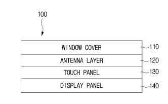
a
conductive ink in the engraved pattern.
[14] The substrate may include at least one of the first panel, the second
panel, and a
separate substrate except for the first panel and the second panel.
[15] The ink layer may be formed with a conductive ink containing the same
kind of
conductive particles.
[16] The conductive particles may have the same size, different sizes, or
different shapes.
[17] The conductive particles may include at least one selected from a
group including
silver (Ag), copper (Cu), nickel (Ni), a silver (Ag)-lead (Pb) alloy, gold
(Au), a gold
(Au)-platinum (Pt) alloy, a copper (Cu)-Nickel (Ni) alloy, and tungsten (W).
[18] The conductive ink may further include blackened particles.
[19] The blackened particles may have a lower specific gravity than the
conductive
particles.
[20] The blackened particles may include at least one selected from a group
including
carbon black, graphite, carbon nanotube, polyacetylene, polypyrrole,
polyaniline, and
polythiophene.
[21] The first panel and the second panel may include at least one of a
display panel, a
touch panel, and a window cover.
[22] The window cover may further include a window protection coating layer
disposed
to be opposite to the window cover, and the antenna layer may be disposed
between
the window protection coating layer and the window cover.
[23] The display panel may include a plurality of panels including a
polarizing panel, and
the antenna layer may be disposed between the plurality of panels.
[24] The display panel may include at least one of a Liquid Crystal Display
(LCD), a re-
flective display, an E-ink display, a Passive Matrix Organic Light Emitting
Diode (PM
OLED) display, and an Active Matrix Organic Light Emitting Diode (AM OLED)
display.
3
CA 02985167 2017-11-06
WO 2016/190506 PCT/KR2015/013848
[25] In accordance with an aspect of the present disclosure, a display
module includes: a
first panel; a second panel disposed to be opposite to the first panel; and an
antenna
layer disposed between the first panel and the second panel, wherein the
antenna layer
includes an ink layer formed with a conductive ink containing the same kind of
conductive particles.
[26] The ink layer may include a conductive material having the same size,
or different
sizes and different shapes.
[27] The conductive material may include at least one selected from a group
including
silver (Ag), copper (Cu), nickel (Ni), a silver (Ag)-lead (Pb) alloy, gold
(Au), a gold
(Au)-platinum (Pt) alloy, a gold (Au)-lead (Pb) alloy, a copper (Cu)-Nickel
(Ni) alloy,
and tungsten (W).
[28] The conductive material may further include a blackened material.
[29] The blackened material may have a lower specific gravity than the
conductive
material.
[30] The blackened material may include at least one selected from a group
including
carbon black, graphite, carbon nanotube, polyacetylene, polypyrrole,
polyaniline, and
polythiophene.
[31] The first panel and the second panel may include at least one of a
window protection
coating layer, a display panel, a touch panel, and a window cover.
[32] In accordance with an aspect of the present disclosure, a display
module includes: a
first panel; a second panel disposed to be opposite to the first panel; and an
antenna
layer disposed between the first panel and the second panel, wherein the
antenna layer
includes a blackened layer formed with the same kind of a conductive material
and a
blackened material having a lower specific gravity than the conductive
material.
[33] The blackened material may include at least one selected from a group
including
carbon black, graphite, carbon nanotube, polyacetylene, polypyrrole,
polyaniline, and
polythiophene.
[34] The conductive material may have the same size, or different sizes and
different
shapes.
[35] The conductive material may include at least one selected from a group
including
silver (Ag), copper (Cu), nickel (Ni), a silver (Ag)-lead (Pb) alloy, gold
(Au), a gold
(Au)-platinum (Pt) alloy, a gold (Au)-lead (Pb) alloy, a copper (Cu)-Nickel
(Ni) alloy,
and tungsten (W).
[36] The first panel and the second panel may include at least one of a
display panel, a
touch panel, and a window cover.
[37] In accordance with an aspect of the present disclosure, a display
module includes: a
first panel; a second panel disposed to be opposite to the first panel; and an
antenna
layer disposed between the first panel and the second panel, and comprising a
resin
4
CA 02985167 2017-11-06
WO 2016/190506 PCT/KR2015/013848
layer formed in a mesh pattern by an imprinting method, wherein the resin
layer
includes: an engraved pattern formed in one surface; and a blackened layer
formed
with the same kind of a conductive material filled in the engraved pattern and
a
blackened material having a lower specific gravity than the conductive
material.
[38] The first panel and the second panel may include at least one selected
from a group
including a window protection coating layer, a window cover, a touch panel,
and a
display panel.
[39] In accordance with an aspect of the present disclosure, a method of
manufacturing a
display module, the display module including a first panel and a second panel,
the
method includes: forming an antenna layer on one surface of the first panel
using an
imprinting method; and coupling the first panel with the second panel, wherein
the
forming of the antenna layer includes: applying a resin on the first panel;
pressing the
applied resin to form an engraved pattern; and applying a conductive ink in
the
engraved pattern to form an antenna layer.
[40] The applying of the conductive ink may include applying a conductive
ink containing
the same kind of conductive particles.
[41] The conductive particles may have the same size, different sizes, or
different shapes.
[42] The conductive particles may include at least one selected from a
group including
silver (Ag), copper (Cu), nickel (Ni), a silver (Ag)-lead (Pb) alloy, gold
(Au), a gold
(Au)-platinum (Pt) alloy, a gold (Au)-lead (Pb) alloy, a copper (Cu)-Nickel
(Ni) alloy,
and tungsten (W).
[43] The conductive ink may further include blackened particles having a
lower specific
gravity than the conductive particles.
[44] The blackened particles may include at least one selected from a group
including
carbon black, graphite, carbon nanotube, polyacetylene, polypyrrole,
polyaniline, and
polythiophene.
[45] The first panel and the second panel may include at least one selected
from a group
including a window protection coating layer, a window cover, a touch panel,
and a
display panel.
Advantageous Effects of Invention
[46] Because the display module according to an aspect includes a
transparent antenna, it
is possible to ensure improved transmission and reception performance.
[47] Also, by forming the transparent antenna with a conductive ink
containing
conductive particles of different sizes, it is possible to improve
conductivity of the
antenna, and to ensure improved transmission and reception performance through
noise reduction.
[48] Also, by blackening the surface of the transparent antenna, it is
possible to prevent
5
CA 02985167 2017-11-06
WO 2016/190506 PCT/KR2015/013848
reflection of light incident from the outside, and to ensure visibility of the
electronic
device (for example, a display device).
Brief Description of Drawings
[49] These and/or other aspects will become apparent and more readily
appreciated from
the following description of exemplary embodiments, taken in conjunction with
the ac-
companying drawings of which:
[50] FIGS. lA and 1B are perspective views of electronic devices according
to em-
bodiments of the present disclosure;
[51] FIG. 2 is a cross-sectional view of the electronic device shown in
FIG. 1B, cut along
a line A-A';
[52] FIGS. 3A and 3B show examples of layered structures of a display
module according
to an embodiment of the present disclosure;
[53] FIG. 4 shows an example of a mesh pattern formed in an antenna layer
according to
an embodiment of the present disclosure;
[54] FIG. 5A, 5B, 5C, and 5D show various modifications of the mesh pattern
shown in
FIG. 4;
[55] FIG. 6 is a cross-sectional view of the antenna layer shown in FIG. 4,
cut along a line
B-B';
[56] FIG. 7 is a view for describing a relationship between the shape of a
mesh pattern
and transmission and reception performance of an antenna layer;
[57] FIG. 8 shows a detailed structure of a display module according to an
embodiment of
the present disclosure, and various arrangement examples of an antenna layer
included
in the display module;
[58] FIG. 9 shows a layered structure of a display module according to an
embodiment of
the present disclosure;
[59] FIG. 10 shows a detailed structure of a display module according to an
embodiment
of the present disclosure, and various formation examples of an antenna layer
included
in the display module;
[60] FIG. 11 shows an example in which conductive particles of the same
size are
provided;
[61] FIG. 12 shows an example in which conductive particles of different
sizes are
provided;
[62] FIG. 13 shows an example in which conductive particles of different
sizes and shapes
are provided;
[63] FIG. 14 is a view for describing a blackening process according to an
embodiment of
the present disclosure;
[64] FIG. 15 is a flowchart illustrating a method of manufacturing a
display module
6
CA 02985167 2017-11-06
WO 2016/190506
PCT/KR2015/013848
according to an embodiment of the present disclosure; and
[65] FIG. 16 is a schematic view for describing the manufacturing method of
FIG. 15.
Best Mode for Carrying out the Invention
[66] Reference will now be made in detail to the embodiments, examples of
which are il-
lustrated in the accompanying drawings, wherein like reference numerals refer
to like
elements throughout. The embodiments are described below to explain the
present
disclosure by referring to the figures.
[67] Hereinafter, a display module, and a method of manufacturing the same
will be
described in detail with reference to the accompanying drawings.
[68] A display module according to an embodiment of the present disclosure
may be
applied to various kinds of electronic devices. The electronic device may be
an
electronic device with a communication function. For example, the electronic
device
may be at least one of a smart phone, a tablet Personal Computer (PC), a
mobile
phone, a video phone, an e-Book reader, a desktop PC, a Personal Digital
Assistant
(PDA), a Portable Multimedia Player (PMP), an MPEG audio layer-3 (MP3) player,
mobile medical equipment, a camera, or a wearable device (for example, a Head-
Mounted-Device (HMD) such as electronic glasses, electronic clothes, an
electronic
bracelet, an electronic necklace, an electronic Appcessory, or a smart watch).
[69] According to some embodiments, the electronic device may be a smart
home
appliance with a communication function. The smart home appliance may be at
least
one of a Television (TV), a Digital Versatile Disk (DVD) player, audio
equipment, a
refrigerator, an air conditioner, a cleaner, an oven, a microwave, a washing
machine,
an air cleaner, a set-top box, a TV box (for example, Samsung HomeSyncTM,
Apple
TVTm, or Google TVTm), game consoles, an electronic dictionary, a camcorder,
or an
electronic album.
[70] According to some embodiments, the electronic device may be at least
one of various
medical equipment (for example, Magnetic Resonance Angiography (MRA), Magnetic
Resonance Imaging (MRI), Computed Tomography (CT), medical camcorder, ul-
trasonic equipment, and the like), a navigation device, a Global Positioning
System
(GPS) receiver, an Event Data Recorder (EDR), a Flight Data Recorder (FDR), an
au-
tomotive infotainment device, electronic equipment for a ship (for example, a
marine
navigation device, a gyro compass, and the like), avionics, or security
equipment.
[71] According to some embodiments, the electronic device may be at least
one of
furniture or part of building/structure with a communication function, an
electronic
board, an electronic signature receiving device, a projector, or various
metering
equipment (for example, water, electricity, gas, or waves metering equipment).
1721
However, the electronic device that can adopt the display module according to
an
7
CA 02985167 2017-11-06
WO 2016/190506 PCT/KR2015/013848
embodiment of the present disclosure is not limited to the aforementioned
devices.
Hereinafter, for convenience of description, the display module will be
described in
detail using a smart watch and a smart phone among the above-mentioned
electronic
devices as examples.
[73] FIG. lA is a perspective view of a smart watch which is an example of
an electronic
device according to an embodiment of the present disclosure, and FIG. 1B is a
per-
spective view of a smart phone which is an example of an electronic device
according
to an embodiment of the present disclosure. As shown in FIGS. lA and 1B, an
electronic device 1 (more specifically, a smart watch la and a smart phone lb)
according to an embodiment of the present disclosure may include a display
module
100, a speaker 2, at least one sensor 3, at least one key 4, and an external
connector
connecting jack 5.
[74] The display module 100 may display images. The display module 100 may
receive
touch inputs. The display module 100 may include an antenna, and in this case,
the
antenna may be transparent in order to ensure visibility of the display module
100.
[75] The speaker 2 may convert an electrical signal generated in the
electronic device 1
into a sound signal to output sound.
[76] The at least one sensor 3 may measure a physical quantity, sense an
operation state of
the electronic device 1, and convert the measured or sensed information into
electrical
signals. The at least one sensor 3 may include at least one of a gesture
sensor, a
proximity sensor, a grip sensor, a gyro sensor, an accelerometer, a
geomagnetic sensor,
a pressure sensor, a temperature/humidity sensor, a hall sensor, a RGB (Red,
Green,
Blue) sensor, an ambient light sensor, a biometric sensor, or an Ultra Violet
(UV)
sensor.
[77] The key 4 may include a pressure key or a touch key. The key 4 may
include a key to
adjust volume, and a key to power the device on/off.
[78] The external connector connecting jack 5 may be used as a High-
Definition
Multimedia Interface (HDMI), a Universal Serial Bus (USB), a projector, a port
for
connecting to a D-subminiature (D-sub) cable, or a charging port.
[79] Hereinafter, the display module 100 will be described in more detail
using the smart
phone lb which is an example of the electronic device 1 according to an
embodiment
of the present disclosure.
[80] FIG. 2 is a cross-sectional view of the electronic device 1 (more
specifically, the
smart phone lb) cut along a line A-A', according to an embodiment of the
present
disclosure, FIG. 3A shows a layered structure of the display module 100
according to
an embodiment of the present disclosure, and FIG. 3B shows a layered structure
of a
display module according to an embodiment of the present disclosure.
[81] As shown in FIG. 2, the electronic device 1 cut along the line A-A'
may include the
8
CA 02985167 2017-11-06
WO 2016/190506 PCT/KR2015/013848
display module 100, a housing 6, a main circuit board 7, and a battery 8.
[82] The display module 100 may include a first panel, a second panel that
is opposite to
the first panel, and an antenna layer disposed between the first panel and the
second
panel, which are layers to create images that are displayed on the electronic
device 1.
Herein, the first panel and the second panel may include at least one of a
window
cover, a touch panel, and a display panel. As shown in FIG. 3A, the display
module
100 may have a structure in which a display panel 140, a touch panel 130, an
antenna
layer 120, and a window cover 110 are stacked in this order. However, the
layered
structure of the display module 100 is not limited to the structure shown in
FIG. 3A,
and a display module 100-1 according to an embodiment of the present
disclosure may
have a structure in which a display panel 140, an antenna layer 120, a touch
panel 130,
and a window cover 110 are stacked in the order as shown in FIG. 3B.
Hereinafter, for
convenience of description, it is assumed that the display module 100 has the
structure
shown in FIG. 3A.
[83] The window cover 110 may be provided to protect the display module
100. The
window cover 110 may be made of a transparent material with predetermined
trans-
mittance. The window cover 110 may be made of glass or a transparent plastic
material
having a uniform thickness and transmittance of a predetermined degree or
more.
[84] According to an embodiment, the window cover 110 may be tempered glass
or thin-
film glass into which a protection film is laminated. Alternatively, the
window cover
110 may be a resin film. If the window cover 110 is a resin film, the window
cover 110
may be made of polyethyleneTerephthalate (PET), polymethylmethacrylate (PMMA),
acryl, polycarbonate (PC), polyimide (PI), polyethylene naphthalate (PEN),
triacetate
cellulose (TAC), polyether sulfone (PES), or the like.
[85] When the window cover 110 is a resin film having flexibility, a thin,
light-weight
display module 100 can be implemented. Also, in this case, the display module
100
can be freely bent or flexed so that it can be applied to various kinds of
devices based
on design freedom.
[86] The antenna layer 120, which is provided to ensure transmission and
reception per-
formance of the electronic device 1, may be below the window cover 110. The
antenna
layer 120 may have a metal mesh structure in order to ensure visibility of the
display
module 100.
[87] One surface of the antenna layer 120 on which a mesh pattern is formed
may be
toward the front surface of the display module 100. According to an embodiment
of
the present disclosure, one surface of the antenna layer 120 on which a mesh
pattern is
formed may be toward the back surface of the display module 100. Hereinafter,
one
surface of the electronic device 1 on which images are displayed is defined as
a front
surface, and the other surface of the electronic device 1 is defined as a back
surface.
9
CA 02985167 2017-11-06
WO 2016/190506 PCT/KR2015/013848
[88] The visibility and conductivity of the display module 100 may depend
on how the
mesh pattern of the antenna layer 120 is formed. Also, the conductivity of the
display
module 100 may depend on a kind of a conductive ink used to form the antenna
layer
120. This will be described in more detail, later.
[89] The touch panel 130 may be used to receive touch commands input from a
user. The
touch panel 130 may be below the antenna layer 120. However, the position of
the
touch panel 130 is not limited to this. Also, according to an embodiment of
the present
disclosure, one surface of the touch panel 130 may be coupled with an
electronic
writing sheet (for example, a digitizer).
[90] The display panel 140, which is provided to display images, may be
below the touch
panel 130. The display panel 140 may be at least one of a Liquid Crystal
Display
(LCD), a reflective display, an E-ink display, a Passive Matrix Organic Light
Emitting
Diode (PM OLED) display, and an Active Matrix Organic Light Emitting Diode (AM
OLED) display.
[91] The housing 6 may include a bracket, a back case, and a battery cover.
[92] The bracket may include an upper bracket and a lower bracket, and the
lower bracket
may be fixed at the lower part of the upper bracket. The bracket may be a
mounting
plate to fix and support a plurality of electronic components (for example, a
commu-
nication module, a memory, a processor, an audio device, a speaker, a
microphone, and
the like).
[93] The back case may be coupled with the bracket. The back case may be
separated
from the battery cover, or integrated into the battery cover.
[94] The battery cover may be coupled with the back case to form the back
of the
electronic device 1. The battery cover may include a plurality of hooks at its
edges,
which are fastened with a plurality of hook fastening grooves of the back
case.
[95] The main circuit board 7 (see FIG. 2, for example, a main board or a
mother board)
may include a substrate on which a fundamental circuit and a plurality of
electronic
components are mounted. The main circuit board 7 may set an execution
environment
of the electronic device 1, and enable the electronic device 1 to stably
operate.
According to an embodiment, the main circuit board 7 may be electrically
connected to
the display module 100 to control the display module 100.
[96] The basic structure of the display module 100 has been described
above.
[97] Hereinafter, a shape of the antenna layer 120 for ensuring
transmission and reception
performance of the display module 100 will be described in more detail.
[98] FIG. 4 shows an example of a mesh pattern formed in the antenna layer
120
according to an embodiment of the present disclosure, FIG. 5 shows various
modi-
fications of the mesh pattern shown in FIG. 4, and FIG. 6 is a cross-sectional
view of
the antenna layer 120 shown in FIG. 4, cut along a line B-B'.
10
CA 02985167 2017-11-06
WO 2016/190506 PCT/KR2015/013848
[99] Referring to FIG. 4, the antenna layer 120 may be formed in a mesh
pattern. The
display module 100 may include the antenna layer 120 formed in the mesh
pattern in
order to ensure visibility.
[100] The mesh pattern may be, as shown in FIG. 4, a pattern in which a
plurality of
diamond- or square-shaped patterns are uniformly arranged, wherein when 01<02,
10<01<89 in order to provide an optimal angle allowing Moire avoidance
according
to display characteristics. However, the mesh pattern is not limited to the
pattern
shown in FIG. 4, and various modifications are possible.
[101] As shown in FIG. 5, the mesh pattern may be a pattern in which a
plurality of square-
shaped patterns are uniformly arranged, as shown in FIG. 5A, a pattern in
which a
plurality of square- or rectangle-shaped patterns are uniformly arranged, as
shown in
FIG. 5B, a pattern in which a plurality of hexagon-shaped patterns are
uniformly
arranged, as shown in FIG. 5C, or a non-uniform pattern in which a plurality
of
random polygon shapes are arranged, as shown in FIG. 5D. In the following de-
scription, for convenience of description, the mesh pattern is assumed to be
the pattern
shown in FIG. 4.
[102] As shown in FIG. 6, the antenna layer 120 may include a substrate
121, and a resin
layer 122 formed by an imprinting method. The resin layer 122 may include, in
its one
surface, a plurality of engraved patterns, or groove, 123 (123 for each) and
an ink layer
124 formed by filling a conductive material in the engraved patterns 123. The
engraved
patterns 123 may be formed in a mesh pattern as described above, and
accordingly, the
ink layer 124 may also be formed in a mesh pattern to correspond to the
engraved
patterns 123. The ink layer 124 may function as an electrode structure because
it is
formed with a conductive material. The conductive material will be described
later.
[103] The transmission and reception performance of the antenna layer 120
included in the
display module 100 may depend on a structure of the engraved patterns 123
formed in
the substrate 121, more specifically, the ink layer 124 formed to correspond
to the
engraved patterns 123. In more detail, as the engraved patterns 123 have
narrower
widths and deeper depths, the antenna layer 120 may have better transmission
and
reception performance. Also, as intervals between the engraved patterns 123,
that is,
the lengths of pitches are shorter, the transmission and reception performance
of the
antenna layer 120 may be improved. However, because transmission and reception
performance of the antenna layer 120 and visibility of the display module 100
are in a
trade-off relationship, the width, depth, and pitch of the engraved patterns
123 are
adjusted appropriately.
[104] Hereinafter, a relationship between a structure of the mesh pattern
and transmission
and reception performance of the antenna layer 120 will be described in more
detail.
11051 FIG. 7 is a view for describing a relationship between the shape of
the mesh pattern
11
CA 02985167 2017-11-06
WO 2016/190506 PCT/KR2015/013848
and transmission and reception performance of the antenna layer 120.
[106] Referring to FIG. 7, the width of an engraved pattern 123 is defined
as a width W,
the thickness of an engraved pattern 123 is defined as a depth D, and an
interval
between two neighboring engraved patterns 123 is defined as a pitch P.
According to
an embodiment, when a plurality of patterns under different pattern
regulations are
combined to form a mesh pattern, an interval between pattern groups under the
different pattern regulations is defined as a pitch, and when a plurality of
diamond-
shaped patterns are combined to form a mesh pattern, a straight distance
between two
neighboring patterns is defined as a pitch.
[107] Meanwhile, a height to width ratio is defined as an aspect ratio.
Generally, if an
aspect ratio is high, it is possible to improve conductivity due to an
increase of the
cross-sectional areas of conductors, while minimizing a reduction rate of
visibility of
the display. However, if an aspect ratio is excessively high, it may be
difficult to
ensure visibility due to a poor viewing angle. Accordingly, an aspect ratio is
appro-
priately adjusted in consideration of both visibility and conductivity.
[108] Each pattern included in the antenna layer 120 may have a width in a
range of ap-
proximately l[im to approximately 10[1m. Generally, if the width of a pattern
is below
1.8 [im, it is difficult to recognize the pattern with a human's naked eyes.
Accordingly,
by reducing the widths of the patterns, visibility of the display module 100
can be
improved. However, if the widths of the patterns are excessively reduced, the
metal
mesh structure may fail to ensure conductivity due to a decrease of the cross-
sectional
areas of the conductors. Accordingly, a lower limit on the widths of the
patterns may
be set to l[im or more.
[109] According to an embodiment, if the widths of the patterns are wide,
an advantage
may be acquired in view of conductivity of the ink layer 124, which may lead
to
ensuring transmission and reception performance of the antenna layer 120.
However, if
the widths of the patterns are excessively wide, a user can see the patterns
with his/her
naked eyes, which may lead to failing to ensure visibility of the display
module 100.
Accordingly, an upper limit on the widths of the patterns may be set to 10[1m
or less.
[110] Each pattern may have a depth in a range of approximately l[im to
approximately
18.5m. Generally, if a depth to width ratio of a pattern is great, an
advantage can be
obtained in view of visibility. For example, comparing a case in which the
width of a
pattern is 2 [im and the depth of the pattern is 4[1m to a case in which the
width of a
pattern is 4 [im and the depth of the pattern is 2[1m, the former case shows
higher
visibility than the latter case, while the two cases show the same
conductivity. This is
because a pattern area that a human's naked eyes can recognize is small.
Accordingly,
the depths of patterns may be adjusted in consideration of the widths of the
patterns.
[111] Meanwhile, if an aspect ratio of the patterns is excessively great, a
viewing angle
12
CA 02985167 2017-11-06
WO 2016/190506 PCT/KR2015/013848
may be limited due to the deep depths of the patterns. Accordingly, the depths
of the
patterns may be set to 18.5[1m or less.
[112] The patterns may have a pitch in a range of approximately 50[1m to
approximately
250m. If the length of the pitch is short, a density of metal per unit area
may increase
to improve conductivity of the electrode structure. However, if the length of
the pitch
is excessively short, visibility may deteriorate. Accordingly, a lower limit
on the pitch
may be set to 50[1m or more.
[113] Meanwhile, if the length of the pitch is excessively long, density of
metal per unit
area may decrease to make ensuring conductivity of the electrode structure
difficult.
Accordingly, an upper limit on the pitch may be set to 250[1m or less.
[114] Hereinafter, a relationship between the structure of the mesh pattern
and transmission
and reception performance of the antenna layer 120 will be described with
reference to
experimental data.
[115] Resistance values of the antenna layer 120 according to various
structures of the
mesh pattern are shown in Table 1, below.
[116] [Table 11
Sample Width (pm) Depth (pm) Pitch (pm) Resistance (n)
Sample 1 5.2 4.5 196 9.73
Sample 2 5.2 4.5 160 8.09
Sample 3 5.2 4.5 130 6.84
Sample 4 5.2 4.5 98 4.95
Sample 5 3.4 6.4 90 4.7
Sample 6 3.7 6.4 110 5.3
Sample 7 3.9 6.1 130 6.2
Sample 8 4.2 6.3 130 5.6
[117] Resistance values shown in Table 1 are resistance values measured on
Samples 1 to 8
13
CA 02985167 2017-11-06
WO 2016/190506 PCT/KR2015/013848
each having a size of 4*60mm in which mesh patterns having widths, depths, and
pitches as shown in Table 1 are respectively formed.
[118] Comparing Samples 1 to 4 to each other, it can be seen that if the
lengths of the
pitches are shortened from 196[1m to 98[1m when the widths and depths of the
mesh
patterns are 5.2[1m and 4.5m, respectively, the resistance values of Samples 1
to 4 are
reduced from 9.73Q to 4.95Q. That is, as the length of a pitch is shortened,
electrical
conductivity of the antenna layer 120 can be improved.
[119] Comparing Samples 3, 7, and 8 to each other, it can be seen that if
the widths of the
mesh patterns are reduced from 5.2[1m to 4.2[1m and the depths of the mesh
patterns
increase from 4.5[1m to 6.3[1m when the pitches of the mesh patterns are the
same as
130m, the resistance values of Samples 3, 7, and 8 are reduced from 6.84Q to
5.6Q.
That is, as the width of a mesh pattern is reduced and the depth of the mesh
pattern
increases, electrical conductivity of the antenna layer 120 can be improved.
[120] The structure of the antenna layer 120 has been described above.
[121] The antenna layer 120 may be disposed between the window cover 110
and the touch
panel 130 of the display module 100. However, the antenna layer 120 of the
display
module 100 may be disposed at another position than between the window cover
110
and the touch panel 130, according to an embodiment.
[122] FIG. 8 shows a detailed structure of the display module 100 according
to an em-
bodiment of the present disclosure, and various arrangement examples of the
antenna
layer 120 included in the display module 100.
[123] Referring to FIG. 8, the display module 100 according to an
embodiment of the
present disclosure may include a window protection coating layer 111 and a
plurality
of adhesive layers 112 and 113, in addition to the components shown in FIGS.
3A and
3B.
[124] The window protection coating layer 111 may be formed on the window
cover 110 to
protect the window cover 110. Also, the first and second adhesive layers 112
and 113
may be disposed between the window cover 110 and the touch panel 130 and
between
the touch panel 130 and the display panel 140, respectively. The first and
second
adhesive layers 112 and 113 may be provided between the individual layers to
fa-
cilitate attachment of the layers while isolating the layers. The first and
second
adhesive layers 112 and 113 may include an Optical Clear Adhesive (OCA) film,
although the disclosure is not limited to this.
[125] The antenna layer 120 may be disposed between the individual layers
shown in FIG.
8. More specifically, the antenna layer 120 may be disposed between the window
protection coating layer 111 and the window cover 110 (P1), between the window
cover 110 and the first adhesive layer 112 (P2), between the first adhesive
layer 112
and the touch panel 130 (P3), between the touch panel 130 and the second
adhesive
14
CA 02985167 2017-11-06
WO 2016/190506 PCT/KR2015/013848
layer 113 (P4), or between the second adhesive layer 113 and the display panel
140
(P5).
[126] According to an embodiment, if the display panel 140 is an OLED type,
the display
panel 140 may include a polarizing film 141 and an organic light emitting
layer 142. In
this case, the antenna layer 120 may be also disposed between the polarizing
film 141
and the organic light emitting layer 142 (P6).
[127] When the antenna layer 120 is disposed at each position P1 to P6, the
antenna layer
120 may be positioned such that the mesh pattern formed on one surface of the
substrate is toward the front or back surface of the display module 100.
[128] The antenna layer 120 may be provided as a separate layer, as
described above with
reference to FIGS. 1 to 6. However, according to an embodiment, the antenna
layer
120 may be formed directly on one surface of a component that is basically
provided to
the display module 100. For example, a conductive ink may be coated on one
surface
of the window cover 110 to provide a conductive pattern in the form of a thin
film
without having to insert any additional component, which may contribute to
slimming
of the electronic device 1. Hereinafter, a layered structure of a display
module
according to an embodiment of the present disclosure will be described with
reference
to the appended drawings.
[129] FIG. 9 shows a layered structure of a display module according to an
embodiment of
the present disclosure.
[130] Referring to FIG. 9, a display module 100a according to an embodiment
of the
present disclosure may include a window cover 110a, an antenna layer 120a, a
touch
panel 130a, and a display panel 140a. The window cover 110a, the touch panel
130a,
and the display panel 140a may be substantially the same as the window cover
110, the
touch panel 130, and the display panel 140 shown in FIGS. 3A and 3B, and ac-
cordingly, further descriptions thereof will be omitted.
[131] The antenna layer 120a may be formed in a mesh pattern, like the
antenna layer 120
shown in FIGS. 4 and 5, by an imprinting method. More specifically, the
antenna layer
120a may be formed directly on one surface of the window cover 110a, which may
lead to slimming of the display module 100a.
[132] According to some embodiments, the antenna layer 120a may be formed
on a layer
other than the window cover 110a.
[133] FIG. 10 shows a detailed structure of the display module 100a
according to an em-
bodiment of the present disclosure, and various formation examples of the
antenna
layer 120a included in the display module 100a.
[134] Referring to FIG. 10, the display module 100a may include a window
protection
coating layer 111a and a plurality of adhesive layers (that is, a first
adhesive layer 112a
and a second adhesive layer 113a), in addition to the components shown in FIG.
9.
15
CA 02985167 2017-11-06
WO 2016/190506 PCT/KR2015/013848
More specifically, the display module 100a may have a structure in which the
display
panel 140a, the second adhesive layer 113a, the touch panel 130a, the first
adhesive
layer 112a, the window cover 110a, and the window protecting coating layer
111a are
stacked in this order.
[135] The antenna layer 120a may be formed on one surface of each layer
shown in FIG.
10. More specifically, the antenna layer 120a may be formed on the rear
surface of the
window protection coating layer 111a (P1), on the front surface of the window
cover
110a (P2), on the rear surface of the window cover 110a (P3), on the front
surface of
the touch panel 130a (P6), on the rear surface of the touch panel 130a (P7),
or on the
front surface of the display panel 140a (P10).
[136] According to an embodiment, if the display panel 140a is an OLED
type, the display
panel 140a may include a polarizing film 141a and an organic light emitting
layer
142a. In this case, the antenna layer 120a may be also formed on one surface
of the po-
larizing film 141a or the organic light emitting layer 142a (P11 and P12).
[137] Examples in which the antenna layer 120 or 120a is disposed (formed)
in the display
module 100 or 100a according to the embodiment of the present disclosure have
been
described above.
[138] The antenna layer 120 or 120a may be formed with a transparent,
conductive
material in order to ensure visibility of the display module 100 or 100a. The
transparent, conductive material may be a conductive ink having low resistance
in
order to ensure transmission and reception performance of an antenna.
[139] Transparency and transmission and reception performance of the
antenna layer 120
or 120a may depend on a mixing proportion of the conductive ink used to form
the
antenna layer 120 or 120a, a kind of conductive particles included in the
conductive
ink, etc. Hereinafter, the conductive ink used to form the antenna layer 120
or 120a
will be described in detail.
[140] The conductive ink according to an embodiment of the present
disclosure may
contain the same kind of conductive particles. The same kind of conductive
particles
may have the same size. However, according to an embodiment, the same kind of
conductive particles may have different sizes and shapes.
[141] FIG. 11 shows an example in which conductive particles of the same
size are
provided, FIG. 12 shows an example in which conductive particles of different
sizes
are provided, and FIG. 13 shows an example in which conductive particles of
different
sizes and shapes are provided.
[142] In FIGS. 11, 12, and 13, the left drawings show states in which a
conductive ink is
filled in an engraved pattern 123, and the right drawings show states in which
conductive particles are connected due to heat generated by post-processing of
applying heat, light, or pressure to the conductive ink, or due to heat
generated by re-
16
CA 02985167 2017-11-06
WO 2016/190506 PCT/KR2015/013848
sistance of the conductive particles when power is supplied to the conductive
particles.
[143] As shown in FIG. 11, the conductive ink may contain conductive
particles of the
same size. Generally, as the size of conductive particles is great, contact
points are
reduced to reduce conductivity, and as the size of conductive particles is
small, surface
resistance increases to reduce conductivity. Accordingly, the conductive ink
according
to the current embodiment may contain conductive particles of the same size.
[144] The conductive particles may melt at different temperatures according
to their sizes.
Because the conductive ink according to the current embodiment contains
conductive
particles of the same size, it is easy to adjust a melting temperature of the
conductive
particles. Accordingly, if the conductive ink according to the current
embodiment is
used in a process of manufacturing the antenna layer 120 or 120a, it may be
easy to
adjust a melting temperature of the conductive ink when the conductive ink was
hardened.
[145] As shown in FIG. 12, the conductive ink may contain first particles
D1 and second
particles D2, wherein the size of the first particles D1 may be different from
that of the
second particles D2. More specifically, a mean particle size of the first
particles D1
may be greater than that of the second particles D2. According to an
embodiment, a
mean particle size of the first particles D1 may be 1 to 1500 times greater
than that of
the second particles D2. However, the mean particle sizes of the first
particles D1 and
the second particle D2 are not limited to the above-mentioned value range.
[146] As shown in FIG. 12, because the conductive ink contains conductive
particles of
different sizes, the conductive ink may have different mean particle sizes per
unit
distance. As a result, the conductive ink can be filled with high density in a
target area
(for example, in the engraved pattern 123). .
[147] Also, by filling the first particles D1 having the greater mean
particle size per unit
distance, electrical contact resistance may be reduced, and as a result,
conductivity of
the antenna layer 120 or 120a may be improved due to an ink layer 124
resulting from
hardening of the conductive ink. Also, the second particles D2 having the
smaller size
may be filled between the first particles D1 having the greater size to
increase density
of metal.
[148] Also, the first and second particles D1 and D2 may have nano sizes.
However, the
sizes and shapes of the first and second particles D1 and D2 are not limited
to nano
sizes, and the first and second particles D1 and D2 may have sizes of several
hundreds
of picometers to several hundreds of micrometers.
[149] As shown in FIG. 13, the conductive ink may contain third particles
D3 and fourth
particles D4, wherein the shape of the third particles D3 may be different
from that of
the fourth particles D4. The third particles D3 may be in the shape of nano
dots, and
the fourth particles D4 may be in the shape of nano rods. Unlike the nano dots
that are
17
CA 02985167 2017-11-06
WO 2016/190506 PCT/KR2015/013848
point-to-point coupled, the nano rods may allow electrical conduction to a
relatively
long distance due to a high aspect ratio. Accordingly, contact resistance at
contact
areas between the particles may be reduced, and as a result, conductivity of
the antenna
layer 120 or 120a can be improved by the ink layer 124 resulting from
hardening of the
conductive ink.
[150] According to an embodiment, the conductive ink may contain conductive
particles in
the shape of nano dots, and a metallic complex compound. In this case, after
the
conductive ink is dried, the metallic complex compound may resolve into a
metal to
surround the nano dots, which reduces contact resistance between the nano dots
to
thereby improve conductivity.
[151] The conductive particles may include particles for low temperature
and particles for
high temperature. More specifically, the particles for low temperature may be
at least
one selected from a group including silver (Ag), copper (Cu), and Nickel (Ni),
and the
particles for high temperature may be at least one selected from a group
including a
silver (Ag)-lead (Pb) alloy, gold (Au), a gold (Au)-platinum (Pt) alloy, a
gold
(Au)-lead (Pb) alloy, a copper (Cu)-Nickel (Ni) alloy, and tungsten (W).
However, the
conductive particles are not limited to the above-mentioned examples.
[152] Meanwhile, if the antenna layer 120 or 120a is formed with a polished
metal
material, light incident from the outside or image light output from the
display panel
may be reflected from the antenna layer 120 or 120a, which may deteriorate a
contrast
ratio.
[153] For this reason, in the display module 100 or 100a according to the
embodiment of
the present disclosure, a blackened layer may be formed on the surface of the
antenna
layer 120 or 120a in order to suppress reflection of light incident from the
outside.
[154] The blackened layer may be formed by including a blackening material
in a
conductive ink provided to form the antenna layer 120 or 120a. Hereinafter, a
case in
which a blackening material is included in a conductive ink will be described
in detail.
[155] The conductive ink according to an embodiment of the present
disclosure may
further include a blackened material, in addition to the conductive particles
described
above. The blackened material may be added in powder form in the conductive
ink. In
the following description, the blackened material added in powder form will be
referred to as blackened particles.
[156] The conductive ink may include approximately 10 to approximately 75
parts of
weight of a solvent and approximately 25 to approximately 90 parts of weight
of a
solid with respect to the entire weight of the conductive ink, and the solid
may include
approximately 80 to approximately 99 parts of weight of conductive particles
and ap-
proximately 1 to approximately 20 parts of weight of blackened particles with
respect
to the entire weight of the solid. In other words, the conductive ink may
include ap-
18
CA 02985167 2017-11-06
WO 2016/190506 PCT/KR2015/013848
proximately 10 to approximately 75 parts of weight of a solvent, approximately
40 to
approximately 89.1 parts of weight of conductive particles, and approximately
0.5 to
approximately 18 parts of weight of blackened particles with respect to the
entire
weight of the conductive ink.
[157] The conductive particles may include, as described above, particles
for low tem-
perature and particles for high temperature. Hereinafter, repetitive
descriptions about
the kinds of the conductive particles will be omitted.
[158] The blackened particles may be at least one selected from a group
including carbon
black, graphite, carbon nanotube, polyacetylene, polypyrrole, polyaniline, and
poly-
thiophene.
[159] The blackened particles may be included at an appropriate proportion
in the
conductive ink. More specifically, if a small amount of the blackened material
is
included in the conductive ink, light incident from the outside may be
reflected from
the surface of the antenna layer 120 or 120a, which may make ensuring
visibility
difficult. Meanwhile, if a large amount of the blackened material is included
in the
conductive ink, a proportion of the conductive particles in the conductive ink
may be
relatively lowered, which may make ensuring conductivity difficult.
Accordingly, a
proportion of the blackened material is appropriately adjusted in the
conductive ink.
[160] The blackened particles may have a lower specific gravity than the
conductive
particles. According to an embodiment, the blackened particles may be graphite
particles having a specific gravity of approximately 1.6. The conductive
particles may
be silver (Ag) particles having a specific gravity of approximately 10.49,
gold (Au)
particles having a specific gravity of approximately 19.29, lead (Pb)
particles having a
specific gravity of approximately 11.34, copper (Cu) particles having a
specific gravity
of approximately 8.93, nickel (Ni) particles having a specific gravity of
approximately
8.9, or platinum (Pt) particles having a specific gravity of approximately
21.45.
[161] As a result, a density of the conductive particles may be within a
range of ap-
proximately 0.1 to approximately 20g/cm3, and may be within a range of ap-
proximately 2.7 to approximately 20g/cm3. Also, a density of the blackened
particles
may be within a range of approximately 0.1 to approximately 1.5 g/cm3.
[162] In the antenna layer 120 or 120a according to the embodiment of the
present
disclosure, a blackened layer may be formed on the surface of the ink layer
124 due to
a specific gravity difference between the conductive particles and the
blackened
particles. FIG. 14 is a view for describing a blackening process according to
an em-
bodiment of the present disclosure.
[163] As shown in FIG. 14, when the conductive ink is filled in the
engraved pattern 123
formed by an imprinting method, the conductive particles D having a relatively
high
specific gravity may sink to the lower part of the engraved pattern 123 by
gravity, and
19
CA 02985167 2017-11-06
WO 2016/190506 PCT/KR2015/013848
the blackened particles B having a relatively low specific gravity may float
on the
upper part of the engraved pattern 123.
[164] In this state, if the conductive ink is hardened, the blackened
particles B positioned
above the conductive particles D may be hardened to form the blackened layer
125 on
the surface of an ink layer 125. In this way, the surface of the antenna layer
120 or
120a can be blackened by a single process.
[165] The blackened particles B and the conductive particles D may have the
same size.
However, according to an embodiment, the blackened particles B and the
conductive
particles D may have different sizes. Also, the conductive particles D may
have the
same size or different sizes. Hereinafter, repetitive descriptions about those
described
above with reference to FIGS. 11 to 13 will be omitted.
[166] Meanwhile, the conductive ink may further include a binder and an
additive.
[167] The binder may be used to facilitate close contacts between the
conductive particles
D. The binder may be at least one selected from a group including phenol,
acryl,
urethane, epoxy, melamine, glass frit, and fluorosilicate. More specifically,
if
conductive particles for low temperature are a main part of the conductive
ink, a
binder, such as phenol, acryl, urethane, epoxy, and melamine, may be used, and
if
conductive particles for high temperature are a main part of the conductive
ink, a
binder, such as glass frit and fluorosilicate, may be used.
[168] The additive may be added to disperse particles or improve printing
quality. The
additive may be at least one selected from a group including 4000 series of
EFKA,
Disprebyk series of BYK, Solsperse series of Avecia, TEGO Disperse series of
Deguessa, Disperse-AYD series of Elementis, JONCRYL series of Johnson Polymer,
Ethyl Cellulose, and Acryl. However, the additive is not limited to the above-
mentioned materials.
[169] The structure of the display module 100 or 100a according to the
embodiment of the
present disclosure has been described above.
[170] Hereinafter, a method of manufacturing the display module 100 or 100a
will be
described.
[171] FIG. 15 is a flowchart illustrating a method of manufacturing a
display module
according to an embodiment of the present disclosure, and FIG. 16 is a
schematic view
for describing the manufacturing method of FIG. 15.
[172] Hereinafter, for convenience of description, on the assumption that
the display
module includes a first panel and a second panel, and the antenna layer 120a
is formed
on one surface of the first panel (see the structure of the display module
100a shown in
FIGS. 9 and 10), a method of manufacturing the display module 100a will be
described.
11731 Referring to FIGS. 15 and 16, the method of manufacturing the display
module 100a
20
CA 02985167 2017-11-06
WO 2016/190506 PCT/KR2015/013848
according to an embodiment of the present disclosure may include operation 200
of
forming the antenna layer 120a on one surface of the first panel by an
imprinting
method, and operation 250 of coupling the first panel with the second panel.
[174] The first panel and the second panel may include the window cover
110a, the touch
panel 130a, and the display panel 140a. According to some embodiments, the
first
panel and the second panel may include, in addition to the window cover 110a,
the
touch panel 130a, and the display panel 140a, a separate substrate (for
example, the
window protection coating layer 111a, the polarizing layer 141a of the display
panel
140a, or the organic light emitting layer 142a) or an adhesive layer 112a or
113a for
making the above-mentioned panels adhere to each other. In the following
description,
the first panel is assumed to be the window cover 110a, and the second panel
is
assumed to be the display panel 140a.
[175] Operation 200 of forming the antenna layer 120a on one surface of the
first panel
110a by the imprinting method may include operation 210 of applying a resin
114 on
the first panel 110a, operation 220 of pressing the applied resin 114 with a
hard stamp
115 and then hardening the resin 114 to form an engraved pattern 123,
operation 230
of applying a conductive ink in the engraved pattern 123, and operation 240 of
hardening the conductive ink.
[176] Operation 210 of applying the resin 114 on one surface of the first
panel 110a may
include applying the resin 114 on one surface of the window cover 110a.
[177] The window cover 110a may be a transparent window cover having a
predetermined
transmittance. The window cover 110a may be glass having a uniform thickness
and
transmittance of a predetermined degree or more. Hereinafter, repetitive
descriptions
about the window cover 110a as described above with reference to FIG. 3 will
be
omitted.
[178] The resin 114 may be a UV resin having predetermined viscosity, or a
transparent,
thermosetting resin. By applying the resin 114 on one surface of the window
cover
110a, and flattening the resin 114 out with a blade having a predetermined
width, a
resin layer 114a having a uniform height and thickness may be formed. In the
current
embodiment, by applying the resin 114 directly on one surface of the window
cover
110a, no additional member for forming the antenna layer 120a may be needed,
which
may lead to slimming of the electronic device 1.
[179] Then, the applied resin 114 may be pressed with the hard stamp 115 to
form the
engraved pattern 123 (operation 220). Herein, the hard stamp 115 may be made
of a
polydimethylsiloxane (PDMS) material. In one surface of the hard stamp 115, a
mi-
cropattern may be formed. By pressing the resin layer 114a with the hard stamp
115
having the micropattern at one surface, and then hardening the resin layer
114a, an
engraved pattern corresponding to the micropattern may be formed on the resin
layer
21
CA 02985167 2017-11-06
WO 2016/190506 PCT/KR2015/013848
114.
[180] The engraved pattern 123 may be in the form of a mesh pattern.
According to an em-
bodiment, the mesh pattern may be formed to correspond to the engraved pattern
123,
and the mesh pattern may have a width of approximately 1 to approximately
10[1m, a
depth of approximately 1 to approximately 18.5 [im, and a pitch of
approximately 50 to
approximately 250m. Accordingly, the engraved pattern 123 may be formed to be
greater than the mesh pattern such that the mesh pattern has such a shape as
described
above.
[181] Then, operation 230 of applying a conductive ink in the engraved
pattern 123 may be
performed. The conductive ink having predetermined transmittance and
conductivity
may be filled in the engraved pattern 123 to form an electrode pattern
corresponding to
the engraved pattern 123.
[182] Before operation 230, operation 260 of preparing the conductive ink
may be
performed. The conductive ink may contain the same kind of conductive
particles. The
conductive particles may have the same size, or may have different sizes or
shapes
according to an embodiment. Hereinafter, repetitive descriptions about the
conductive
particles will be omitted.
[183] The conductive particles may include particles for low temperature
and particles for
high temperature. More specifically, the particles for low temperature may be
at least
one selected from a group including silver (Ag), copper (Cu), and Nickel (Ni),
and the
particles for high temperature may be at least one selected from a group
including a
silver (Ag)-lead (Pb) alloy, gold (Au), a gold (Au)-platinum (Pt) alloy, a
gold
(Au)-lead (Pb) alloy, a copper (Cu)-Nickel (Ni) alloy, and tungsten (W).
However, the
conductive particles are not limited to the above-mentioned examples.
[184] By applying the conductive ink and then hardening the conductive ink,
an electrode
pattern may be formed on one surface of the window cover 110a, and the
electrode
pattern may function as the antenna layer 120a.
[185] Then, the first panel 110a in whose one surface the antenna layer
120a is formed may
be coupled with the second panel 140a (operation 250). The second panel 140a
may be
the display panel 140a as described above. More specifically, the second panel
140a
may be at least one of LCD, a reflective display, an E-ink display, a PM OLED
display, and an AM OLED display. However, the display panel 140a is not
limited to
the above-mentioned displays.
[186] Although a few embodiments of the present disclosure have been shown
and
described, it would be appreciated by those skilled in the art that changes
may be made
in these embodiments without departing from the principles and spirit of the
disclosure, the scope of which is defined in the claims and their equivalents.