Note: Descriptions are shown in the official language in which they were submitted.
84111691
- 1 -
INTERPOSER FOR A PACKAGE-ON-PACKAGE STRUCTURE
CROSS-REFERENCE TO RELATED APPLICATIONS
[0001] The present application claims priority from commonly owned U.S. Non-
Provisional Patent
Application No. 14/733,201 filed on June 8, 2015.
FIELD
[0002] The present disclosure is generally related to package-on-package (PoP)
structures.
DESCRIPTION OF RELATED ART
[0003] Advances in technology have resulted in smaller and more powerful
computing devices. For
example, there currently exist a variety of portable personal computing
devices, including wireless
computing devices, such as portable wireless telephones, personal digital
assistants (PDAs), tablet
computers, and paging devices that are small, lightweight, and easily carried
by users. Many such
computing devices include other devices that are incorporated therein. For
example, a wireless
telephone can also include a digital still camera, a digital video camera, a
digital recorder, and an
audio file player. Also, such computing devices can process executable
instructions, including
software applications, such as a web browser application that can be used to
access the Internet and
multimedia applications that utilize a still or video camera and provide
multimedia playback
functionality.
[0004] A wireless device may include memory devices (e.g., memory chips) to
store data. Typical
memory devices may have between approximately 300 and 400 input/output (I/O)
ports. However,
wide I/0 memory devices may have between approximately 1700 and 2000 I/O
ports. Package-on-
package (PoP) techniques may be used to package wide I/0 memory devices (e.g.,
to vertically
combine/stack a wide I/0 memory device with logic circuits or dies) to improve
(e.g., increase)
component density in wireless computing devices.
[0005] A PoP structure may use an interposer as an electrical interface that
routes electrical signals
between one component of the PoP structure and another component of the PoP
structure. For
example, an interposer may be used to route electrical signals between an I/O
port of a wide I/O
memory device of the PoP structure and an associated
Date Recue/Date Received 2022-10-07
CA 02985197 201.7-11-06
WO 2016/200604
PCT/US2016/033948
- 2 -
logic circuit (e.g., die) of the PoP structure. However, a conventional
interposer for a
PoP structure may occupy a relatively large amount of die area, increasing the
package
size of the PoP structure. For example, an interposer may use relatively large
solder
balls to route electrical signals from the I/O ports of the wide I/O memory
device to the
other components of the PoP structure. The solder balls may increase an
interconnect
length between the wide I/O memory device and the other components, which may
degrade signal integrity and power integrity.
SUMMARY
[0006] According to one implementation, a package-on-package (PoP) structure
includes a first die, a second die, and a memory device electrically coupled
to the first
die and the second die by an interposer between the first die and the second
die. The
interposer includes copper-filled vias formed within a mold.
[0007] According to another implementation, a method for forming a package-on-
package (PoP) structure includes coupling a first die and a second die to a
bottom
interposer. The method also includes forming a mold on the first die, the
second die,
and the bottom interposer. The method further includes etching one or more
vias within
the mold. The one or more vias are located between the first die and the
second die.
The method also includes filling the one or more vias with copper to form an
interposer
having one or more copper-filled vias.
[0008] According to another implementation, a non-transitory computer-readable
medium includes data for forming a package-on-package (PoP) structure. The
data,
when used by fabrication equipment, causes the fabrication equipment to couple
a first
die and a second die onto a bottom interposer. The data, when used by the
fabrication
equipment, further cause the fabrication equipment to form a mold on the first
die, the
second die, and the bottom interposer. The data, when used by the fabrication
equipment, also causes the fabrication equipment to etch one or more vias
within the
mold. The one or more vias are located between the first die and the second
die. The
data, when used by the fabrication equipment, further causes the fabrication
equipment
to fill the one or more vias with copper to form an interposer having one or
more
copper-filled vias.
[0009] According to another implementation, a package-on-package (PoP)
structure
includes means for performing a first logical function, means for performing a
second
84111691
- 3 -
logical function, and means for storing data. The means for storing data
coupled to the means for
perfouning the first logical function and coupled to the means for performing
the second logical
function. The PoP structure also includes means for routing electrical signals
between the means for
storing data and at least one of the means for performing the first logical
function or the means for
performing the second logical function. The means for routing electrical
signals is between the
means for performing the first logical function and the means for performing
the second logical
function. The means for routing electrical signals includes copper-filled vias
formed within a mold.
[0009a1 According to one aspect of the present invention, there is provided a
package-on-package
(PoP) structure comprising: a first die; a second die; a mold between the
first die and the second die,
the mold including vias including a barrier/seed deposition layer and copper,
the barrier/seed
deposition layer configured to isolate the copper from the mold; and a bottom
interposer electrically
coupled to the vias, the first die and the second die; a memory device
electrically coupled to the first
die and to the second die by the vias and the bottom interposer.
[0009b] According to another aspect of the present invention, there is
provided a method for
forming a package-on-package (PoP) Mixture, the method comprising: coupling a
first die and a
second die to a bottom interposer; forming a mold on the first die, the second
die, and the bottom
interposer; etching one or more vias within the mold, the one or more vias
located between the first
die and the second die; depositing a barrier/seed deposition layer into the
one or more vias prior to
filling the one or more vias with copper; and filling the one or more vias
with copper to form an
interposer having one or more vias.
[0009c] According to another aspect of the present invention, there is
provided a non-transitory
computer-readable medium comprising computer executable instructions stored
thereon for forming
a package-on-package (PoP) structure, the instructions, when used by
fabrication equipment, causes
the fabrication equipment to: couple a first die and a second die onto a
bottom interposer; form a
mold on the first die, the second die, and the bottom interposer; etch one or
more vias within the
mold, the one or more vias located between the first die and the second die;
and fill the one or more
vias with copper to form an interposer having one or more vias.
10009d] According to another aspect of the present invention, there is
provided a package-on-
package (PoP) structure comprising: means for performing a first logical
function; means for
Date recue/date received 2022-10-11
84111691
- 3a -
performing a second logical function; means for storing data, the means for
storing data coupled to
the means for performing the first logical function and coupled to the means
for performing the
second logical function; and means for routing electrical signals between the
means for storing data
and at least one of the means for performing the first logical function or the
means for performing
the second logical function, the means for routing electrical signals is
between the means for
performing the first logical function and the means for performing the second
logical function, and
the means for routing electrical signals comprising vias formed within a mold,
wherein the vias
include a barrier/seed deposition layer and copper, the barrier/seed
deposition layer configured to
isolate the copper from the mold.
BRIEF DESCRIPTION OF THE DRAWINGS
[0010] FIG. 1 is a diagram of a particular illustrative aspect of a package-on-
package (PoP)
structure having an interposer formed between two dies of a package;
[0011] FIG. 2A illustrates a particular stage of forming the PoP structure of
FIG. 1;
[0012] FIG. 2B illustrates another particular stage of forming the PoP
structure of FIG. 1;
[0013] FIG. 2C illustrates another particular stage of forming the PoP
structure of FIG. 1;
[0014] FIG. 2D illustrates another particular stage of forming the PoP
structure of FIG. 1;
[0015] FIG. 2E illustrates another particular stage of forming the PoP
structure of FIG. 1;
[0016] FIG. 2F illustrates another particular stage of forming the PoP
structure of FIG. 1;
[0017] FIG. 2G illustrates another particular stage of forming the PoP
structure of FIG. 1;
[0018] FIG. 2H illustrates another particular stage of forming the PoP
structure of FIG. 1;
[0019] FIG. 3 is a flowchart of a particular illustrative aspect of a method
for forming a PoP
structure having an interposer for formed between two dies of a package;
100201 FIG. 4 is a block diagram of a device that includes a PoP structure
having an interposer for
formed between two dies of a package; and
Date Recue/Date Received 2022-10-07
CA 02985197 2017-11-06
WO 2016/200604
PCT/US2016/033948
- 4 -
[0021] FIG 5 is a data flow diagram of a particular illustrative aspect of a
manufacturing process to manufacture electronic devices that include a PoP
structure
having an interposer for formed between two dies of a package.
DETAILED DESCRIPTION
[0022] Techniques and methods for forming a package-on-package (PoP) structure
having an interposer formed between two dies of a package are disclosed. For
example,
vias may be etched into a mold (e.g., a dielectric mold) and filled using
copper
electroplating to form the interposer. The interposer may be electrically
coupled to a
bottom interposer of the PoP structure, and the bottom interposer may be
electrically
coupled to a first die and to a second die. The interposer, the first die, and
the second
die are included in a common package of the PoP structure. After the
interposer is
formed and electrically coupled to the bottom interposer, a memory device
(e.g., a wide
input/output (I/O) memory chip) may be attached to the interposer. Electrical
signals
(e.g., data) may be routed between the memory device and the dies by way of
the
interposer.
[0023] One particular advantage provided by at least one of the disclosed
aspects is the
ability to route electrical signals (e.g., data) between a memory chip and
dies of a
package-on-package (PoP) structure using an interposer formed between the
dies.
Using the interposer formed between the dies to route electrical signals
between the
memory chip and the dies may decrease an interconnect length between the
memory
chip and the dies compared to a conventional PoP structure that uses solder
balls (as an
interposer) that occupy a relatively large amount of die area Decreasing the
interconnect length may reduce the package size of the PoP structure compared
to a
conventional PoP structure. Additionally, decreasing the interconnect length
may
improve signal integrity and power integrity.
[0024] Language describing the location of one component with respect the
location of
another component (e.g., on top of, underneath, top, bottom, etc.) refers to
the
orientation of the components in the figures. This language should not be
construed as
limiting. For example, if a structure is rotated, flipped, etc., the location
of a component
with respect to the location of another component change.
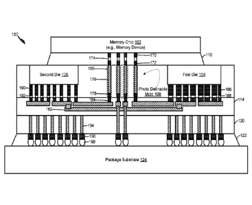
[0025] Referring to FIG 1, a particular illustrative aspect of a package-on-
package
(PoP) structure 100 having an interposer formed between two dies of a package
is
CA 02985197 2017-11-06
WO 2016/200604
PCT/US2016/033948
- 5 -
shown. The PoP structure 100 includes a memory chip 102, a first die 104, a
second die
106, and a photo definable mold 108. In a particular aspect, the memory chip
102 is a
wide input/output (I/0) memory device. For example, the memory chip 102 may
have
between approximately 1700 and 2000 1/0 ports. The memory chip 102 may be
included in a "first package" of the PoP structure 100, and the dies 104, 106
may be
included in a "second package" of the PoP structure 100.
[0026] The first die 104 may include first circuitry (not shown) that is
configured to
perform a first logical function. For example, first data from the memory chip
102 may
be communicated (e.g., as first electrical signals) from the memory chip 102
to the first
circuitry in the first die 104, and the first circuitry may perform the first
logical function
on the first data. After the first logical function is performed on the first
data to produce
first modified data, the first modified data may be communicated to the memory
chip
102.
[0027] In a similar manner, the second die 106 may include second circuitry
(not
shown) that is configured to perform a second logical function. For example,
second
data from the memory chip 102 may be communicated (e.g., as second electrical
signals) from the memory chip 102 to the second circuitry in the second die
106, and the
second circuitry may perform the second logical function on the second data.
After the
second logical function is performed on the second data to produce second
modified
data, the second modified data may be communicated to the memory chip 102.
[0028] As described in greater detail below, the PoP structure 100 utilizes
the photo
definable mold 108 and a bottom interposer 114 to communicate (e.g., transmit)
electrical signals between the memory chip 102 and at least one of the first
die 104 or
the second die 106. An interposer may be formed within the photo definable
mold 108
between the first die 104 and the second die 106. For example, the photo
definable
mold 108 may be included in the same "package" as the first die 104 and the
second die
106. The bottom interposer 114 may be located underneath the photo definable
mold
108 and the dies 104, 106.
[0029] An underfill 110 may be used to connect the memory chip 102 to the
photo
definable mold 108. The underfill 110 may include an epoxy adhesive. For
example,
the first package (e.g., the memory chip 102) may be mounted on top of the
second
package (e.g., the first die 104, the second die 106, and the photo definable
mold 108)
CA 02985197 2017-11-06
WO 2016/200604
PCT/US2016/033948
- 6 -
using the epoxy adhesive. Additionally, pads 170 of the memory chip 102 may be
electrically coupled to top pads 172 of the photo definable mold 108 by
microbumps
174. The microbumps 174 may include copper, tin-silver or tin-silver-copper.
Thus,
data may be communicated (e.g., as electrical signals) between the memory chip
102
and the photo definable mold 108 by the pads 170, 172 and the microbumps 174.
Each
pad 170 of the memory chip 102 may be coupled to an I/O port of the memory
chip 102.
In the implementation of FIG. 1, the memory chip 102 is shown to include four
pads
170. In other implementations, the memory chip 102 may include additional pads
170.
For example, if the memory chip 102 is a wide I/O memory device, the memory
chip
102 may include between approximately 1700 and 2000 pads. Each pad 170 may be
coupled to a corresponding I/O port of the wide VO memory device.
100301 The photo definable mold 108 may include copper-filled vias 176 to form
the
interposer. Each copper-filled via 176 may be electrically coupled to a
corresponding
top pad 172 of the photo definable mold 108. In the implementation of FIG 1,
the
photo definable mold 108 is shown to include four copper-filled vias 176. In
other
implementations, the photo definable mold 108 may include additional copper-
filled
vias. For example, if the memory chip 102 is a wide I/O memory device, the
photo
definable mold 108 may include between approximately 1700 and 2000 copper-
filled
vias. The photo definable mold 108 may also include bottom pads or under bump
metallurgy (UBM) 178 that are electrically coupled to corresponding copper-
filled vias
176. In the implementation of FIG 1, the photo definable mold 108 is shown to
include
four bottom pads 178. Each bottom pad 178 may be coupled to a corresponding
copper-
filled via 176 of the photo definable mold 108. In other implementations, the
photo
definable mold 108 may include additional bottom pads 178. For example, if the
memory chip 102 is a wide I/O memory device, the photo definable mold 108 may
include between approximately 1700 and 2000 bottom pads.
[0031] The copper-filled vias 176 may be located within the photo definable
mold 108.
The photo definable mold 108 may be deposited using lamination or thermal
compression molding techniques. The photo definable mold 108 may include a
material
with a high dielectric constant (e.g., a "photo-dielectric" mode) and the
photo definable
mold 108 may include copper-filled vias 176 A barrier/seed deposition layer
180 may
isolate the copper-filled vias from the photo definable mold 108. The
barrier/seed
CA 02985197 2017-11-06
WO 2016/200604
PCT/US2016/033948
- 7 -
deposition layer 180 may be deposited using PVD techniques. For example, the
barrier/seed deposition layer 180 may be deposited into vias that are photo
defined by
lithography into the photo definable mold 108, and the copper (of the copper-
filled vias
176) may be deposited into the vias using electroplating techniques to form
the copper-
filled vias 176. According to one implementation, the photo definable mold 108
may
include a dielectric mold.
[0032] The photo definable mold 108 may be used to connect the first die 104,
the
second die 106, and the photo definable mold 108 to the bottom interposer 114.
The
bottom interposer 114 may include copper-filled vias 182 and top pads 184 that
are
electrically coupled to the copper-filled vias 176. A subset of top pads 184
of the
bottom interposer 114 may be electrically coupled to the bottom pads 178 of
the photo
definable mold 108 by microbumps (not shown). In the implementation of FIG. 1,
the
bottom interposer 114 is shown to include four top pads 184 that are
electrically coupled
to the four bottom pads 178 of the photo definable mold 108.
[0033] The bottom interposer 114 may provide an electrical connection between
the
photo definable mold 108 and the dies 104, 106. For example, a subset of top
pads 184
of the bottom interposer 114 may be coupled to bottom pads 186 of the first
die 104 by
microbumps 188, and a subset of top pads 184 of the bottom interposer 114 may
be
coupled to bottom pads 190 of the second die 106 by microbumps 192. In the
implementation of FIG 1, eight top pads 184 of the bottom interposer 114 are
shown to
be coupled to eight bottom pads 186 of the first die 104 by eight
corresponding
microbumps 188, and eight top pads 184 of the bottom interposer 114 are shown
to be
coupled to eight bottom pads 190 of the second die 106 by eight corresponding
microbumps 192. In the implementation of FIQ 1, the additional (or fewer) pads
184,
186, 190 and microbumps 188, 192 may be present.
[0034] The bottom interposer 114 may be mounted on a silicon substrate 120,
the
silicon substrate 120 may be mounted on an underfill 122, and the underfill
122 may be
mounted on a package substrate 124. Copper-filled vias 194 may be formed in
the
silicon substrate 120, pads 196 may be electrically coupled to the copper-
filled vias 194
of the silicon substrate 120, and microbumps 198 may electrically couple the
pads 196
to the package substrate 124.
CA 02985197 2017-11-06
WO 2016/200604
PCT/US2016/033948
- 8 -
[0035] The PoP structure 100 of FIG 1 may enable electrical signals (e.g.,
representing
data) to be routed between the memory chip 102 and the dies 104, 106 by way of
the
photo definable mold 108 formed between the dies 104, 106. For example,
electrical
signals may be transmitted from the memory chip 102 to the photo definable
mold 108
using conductivity paths (e.g., the bottom pads 170 of the memory chip 102,
the
microbumps 174, and the top pads 172 of the photo definable mold 108) between
the
memory chip 102 and the photo definable mold 108. The electrical signals may
be
routed through the copper-filled vias 176 of the photo definable mold 108 and
to the
bottom interposer 114 by way of conductivity paths (e.g., the bottom pads 178
of the
photo definable mold 108, the microbumps (not shown), and the top pads 184 of
the
bottom interposer 114) between the photo definable mold 108 and the bottom
interposer
114. The electrical signals may be routed through the copper-filled vias 182
of the
bottom interposer 114 and to either the first die 104 or the second die 116 by
way of
conductivity paths between the bottom interposer 114 and the dies 104, 106.
[0036] Using the photo definable mold 108 fomied between the first and second
dies
104, 106 to route electrical signals between the memory chip 102 and the dies
104, 106
may decrease an interconnect length between the memory chip 102 and the dies
104,
106 compared to a conventional PoP structure that uses solder balls (as an
interposer)
that occupy a relatively large amount of die area. Decreasing the interconnect
length
may reduce the package size of the PoP structure 100 compared to a
conventional PoP
structure. Additionally, decreasing the interconnect length may improve signal
integrity
and power integrity.
[0037] Referring to FIG 2A, a particular stage of forming the PoP structure
100 of FIG
1 is shown. At the stage of FIG 2A, the first die 104 and the second die 106
are coupled
to the bottom interposer 114. For example, the first die 104 may be attached
to the
bottom interposer 114, and the second die 106 may be attached to the bottom
interposer
114. The dies 104, 106 may be attached to the bottom interposer 114 using a
reflow
process (e.g., a thermal process).
[0038] Additionally, at the stage of FIG 2A, a backside of the wafer (e.g.,
the silicon
substrate 120) may be placed on (e.g., attached to) a temporary carrier 204
using
temporary carrier bonding techniques. For example, the temporary carrier 204
may be
CA 02985197 2017-11-06
WO 2016/200604
PCT/US2016/033948
- 9 -
attached to the wafer using a temporary glue 202 (or adhesive). The techniques
of FIG
2A may be performed using the fabrication equipment described with respect to
FIG 5.
[0039] Referring to FIG 2B, another particular stage of forming the PoP
structure 100
of FIG 1 is shown. At the stage of FIG 2B, the photo definable mold 108 (e.g.,
a photo
"pattern-able" mold or polymer) is deposited on top of the first die 104, on
top of the
second die 106, and on top of the bottom interposer 114. The photo definable
mold 108
may be deposited using lamination deposition techniques, thermal compression
molding
techniques, or molding deposition techniques. In one implementation, the photo
definable mold 108 may include a "photo-dielectric" mold. The techniques of
FIG 2B
may be performed using the fabrication equipment described with respect to FIG
S.
[0040] Referring to FIG 2C, another particular stage of forming the PoP
structure 100
of FIG 1 is shown. At the stage of FIG 2C, a plurality of vias may be etched
through
the photo definable mold 108. For example, a photo resist (not shown) may be
deposited (e.g., patterned) on top of the photo definable mold 108 using a
lithography
(e.g., a photolithography) process. After depositing the photo resist,
portions of the
photo resist may be "opened" to pattern areas for a thy etch process, and the
vias may
be etched through the photo definable mold 108 during the dry etch process.
After the
vias are etched through the photo definable mold 108, the phot resist may be
removed.
The vias may be etched using the fabrication equipment described with respect
to FIG
5.
[0041] Referring to FIG 2D, another particular stage of forming the PoP
structure 100
of FIG 1 is shown. At the stage of FIG 2D, seed layers and barrier layers
(e.g., the
barrier/seed deposition layer 180) are deposited into the vias using a
physical vapor
deposition (PVD) process. The seed layers may include copper, and the barrier
layers
may include tantalum or silicon nitride. The techniques of FIG 2D may be
performed
using the fabrication equipment described with respect to FIG 5.
[0042] Referring to FIG 2E, another particular stage of forming the PoP
structure 100
of FIG 1 is shown. At the stage of FIG 2E, a photo resist layer 206 may be
deposited
(e.g., patterned) on top of the barrier/seed deposition layer 180 using a
lithography (e.g.,
photolithography) process. The techniques of FIG 2E may be performed using the
fabrication equipment described with respect to FIG 5.
CA 02985197 2017-11-06
WO 2016/200604
PCT/US2016/033948
- 10 -
[0043] Referring to FIG 2F, another particular stage of forming the PoP
structure 100 of
FIG 1 is shown. At the stage of FIG 2F, the vias are filled with copper using
a copper
electroplating process. The techniques of FIG 2F may be performed using the
fabrication equipment described with respect to FIG 5.
[0044] Referring to FIG 2Q another particular stage of forming the PoP
structure 100
of FIG 1 is shown. At the stage of FIG 2G, the photo resist layer 206 and the
portions
of the barrier/seed deposition layer 180 underneath the photo resist layer 206
may be
removed using a planarization process (e.g., a chemical mechanical
planarization
(CMP) process). For example, the front side of the wafer undergoes
planarization to
expose portions of the photo definable mold 108 that were previously covered
by the
photo resist layer 206. The techniques of FIG 2G may be performed using the
fabrication equipment described with respect to FIG 5.
[0045] Referring to FIG 2H, another particular stage of forming the PoP
structure 100
of FIG 1 is shown. At the stage of FIG 2H, the memory chip 102 is placed on
top of
the photo definable mold 108 and the dies 104, 106 using thermal compression
bonding.
For example, the pads of the memory chip 102 may be attached to top pads of
the photo
definable mold 108 using a thermal heating process (e.g., reflow). After the
thermal
heating process, the underfill 110 may be dispensed between the photo
definable mold
108 and the memory chip 102. In a particular implementation, the undeifill 110
may be
dispensed prior to attaching the memory chip 102. The techniques of FIG 2H may
be
performed using the fabrication equipment described with respect to FIG 5.
[0046] After the memory chip 102 is attached, the temporary carrier 204 may be
detached from the wafer using a temporary carrier debonding process. The
temporary
carrier debonding process may be performed using the fabrication equipment
described
with respect to FIG 5. After the debonding process, the wafer may be deposited
onto
the package substrate 124, as shown in FIG 1.
[0047] The stages described with respect to FIGS. 2A-2H may enable fabrication
of a
structure where electrical signals (e.g., data) are routed between the memory
chip 102
and the dies 104, 106 by way of the photo definable mold 108 formed between
the dies
104, 106. For example, electrical signals may be transmitted from the memory
chip 102
to the photo definable mold 108 using conductivity paths (e.g., the bottom
pads of the
memory chip 102, the microbumps, and the top pads of the photo definable mold
108)
CA 02985197 2017-11-06
WO 2016/200604
PCT/US2016/033948
-11 -
between the memory chip 102 and the photo definable mold 108. The electrical
signals
may be routed through the copper-filled vias of the photo definable mold 108
and to the
bottom interposer 114 by way of conductivity paths (e.g., the bottom pads of
the photo
definable mold 108, the microbumps, and the top pads of the bottom interposer
114)
between the photo definable mold 108 and the bottom interposer 114. The
electrical
signals may be routed through the copper-filled vias of the bottom interposer
114 and to
either the first die 104 or the second die 116 by way of conductivity paths
between the
bottom interposer 114 and the dies 104, 106.
[0048] Using the photo definable mold 108 formed between the first and second
dies
104, 106 to route electrical signals between the memory chip 102 and the dies
104, 106
may decrease an interconnect length between the memory chip 102 and the dies
104,
106 compared to a conventional PoP structure that uses solder balls (as an
interposer)
that occupy a relatively large amount of die area. Decreasing the interconnect
length
may reduce the package size of the PoP structure 100 compared to a
conventional PoP
structure. Additionally, decreasing the interconnect length may improve signal
integrity
and power integrity.
[0049] Referring to FIG 3, a flowchart of a method 300 for forming a PoP
structure
having an interposer between two dies of a package is shown. The method 300
may be
performed using the fabrication equipment described with respect to FIG 5.
[0050] The method 300 includes coupling a first die and a second die to a
bottom
interposer, at 302. For example, referring to FIG 2A, the first die 104 and
the second
die 106 may be coupled to the bottom interposer 114. The dies 104, 106 may be
attached to (e.g., electrically coupled to) the bottom interposer 114 using a
reflow
process (e.g., a thermal process).
[0051] A mold may be formed on the first die, the second die, and the bottom
interposer, at 304. For example, referring to FIG 2B, the photo definable mold
108
(e.g., a photo "pattern-able" mold) may be deposited on the first die 104, on
the second
die 106, and on the bottom interposer 114. The photo definable mold 108 may be
deposited using lamination deposition techniques, thermal compression molding
techniques, or molding deposition techniques. In one implementation, the photo
definable mold 108 may include a photo-dielectric mold.
CA 02985197 2017-11-06
WO 2016/200604
PCT/US2016/033948
- 12 -
[0052] One or more vias may be etched within the mold, at 306. The one or more
vias
may be located between the first die and the second die. For example,
referring to FIG
2C, a plurality of vias may be etched through the photo definable mold 108.
For
example, a photo resist may be deposited (e.g., patterned) on top of the photo
definable
mold 108 using a lithography (e.g., a photolithography) process. After
depositing the
photo resist, portions of the photo resist may be "opened" to pattern areas
for a dry etch
process, and the vias may be etched through the photo definable mold 108
during the
dry etch process.
[0053] According to one implementation, the method 300 may include depositing
a
barrier/seed deposition layer into the one or more vias. For example,
referring to FIG
2D, seed layers and barrier layers (e.g., the barrier/seed deposition layer
180) may be
deposited into the vias using a physical vapor deposition (PVD) process. The
seed
layers may be comprised of copper, and the barrier layers may be comprised of
tantalum
or silicon nitride.
[0054] The one or more via may be filled with copper to form an interposer
having one
or more copper-filled vias, at 308. For example, referring to FIG 2F, the vias
may be
filled with copper using a copper electroplating process. The one or more
copper-filled
vias 176 may be electrically coupled to the bottom interposer 114, and the
bottom
interposer 114 may be electrically coupled to the first die 104 and to the
second die 106.
[0055] According to one implementation, the method 300 may include
electrically
coupling a memory device to the first die, to the second die, and to the
interposer. The
interposer may be configured to route signal between the memory device and at
least
one of the first die or the second die. For example, referring to FIG 2H, the
memory
chip 102 may be coupled to the photo definable mold 108 and the dies 104, 106
using
thermal compression bonding. For example, the pads of the memory chip 102 may
be
attached to top pads of the photo definable mold 108 using a thermal heating
process.
After the thermal heating process, the underfill 110 may be dispensed between
the photo
definable mold 108 and the memory chip 102. In a particular implementation,
the
underfill 110 may be dispensed prior to attaching the memory chip 102.
[0056] The method 300 of FIG 3 may enable electrical signals (e.g., data) to
be routed
between the memory chip 102 and the dies 104, 106 via the photo definable mold
108
formed between the dies 104, 106. For example, electrical signals may be
transmitted
CA 02985197 2017-11-06
WO 2016/200604
PCT/US2016/033948
- 13 -
from the memory chip 102 to the photo definable mold 108 using conductivity
paths
(e.g., the bottom pads of the memory chip 102, the microbumps, and the top
pads of the
photo definable mold 108) between the memory chip 102 and the photo definable
mold
108. The electrical signals may be routed through the copper-filled vias of
the photo
definable mold 108 and to the bottom interposer 114 via conductivity paths
(e.g., the
bottom pads of the photo definable mold 108, the microbumps, and the top pads
of the
bottom interposer 114) between the photo definable mold 108 and the bottom
interposer
114. The electrical signals may be routed through the copper-filled vias of
the bottom
interposer 114 and to either the first die 104 or the second die 116 via
conductivity paths
between the bottom interposer 114 and the dies 104, 106.
[0057] Using the photo definable mold 108 formed between the first and second
dies
104, 106 to route electrical signals between the memory chip 102 and the dies
104, 106
may decrease an interconnect length between the memory chip 102 and the dies
104,
106 compared to a conventional PoP structure that uses solder balls (as an
interposer)
that occupy a relatively large amount of die area. Decreasing the interconnect
length
may reduce the package size of the PoP structure 100 compared to a
conventional PoP
structure. Additionally, decreasing the interconnect length may improve signal
integrity
and power integrity.
[0058] Referring to FIG 4, a particular illustrative aspect of a wireless
communication
device is depicted and generally designated 400. The device 400 includes a
processor
410, such as a digital signal processor, coupled to a memory 432.
[0059] The processor 410 may be configured to execute software (e.g., a
program of
one or more instructions 468) stored in the memory 432. A memory device 490
may be
coupled to the processor 410. The memory device 490 may include the PoP
structure
100 of FIG 1. For example, the PoP structure 100 may include an interposer
formed
between two dies of a single package.
[0060] A wireless interface 440 may be coupled to the processor 410 and to an
antenna
442. A coder/decoder (CODEC) 434 can also be coupled to the processor 410. A
speaker 436 and a microphone 438 can be coupled to the CODEC 434. A display
controller 426 can be coupled to the processor 410 and to a display device
428. In a
particular aspect, the processor 410, the display controller 426, the memory
432, the
CODEC 434, and the wireless interface 440 are included in a system-in-package
or
CA 02985197 2017-11-06
WO 2016/200604
PCT/US2016/033948
- 14 -
system-on-chip device 422. In a particular aspect, an input device 430 and a
power
supply 444 are coupled to the system-on-chip device 422. Moreover, in a
particular
aspect, as illustrated in FIG 4, the display device 428, the input device 430,
the speaker
436, the microphone 438, the antenna 442, and the power supply 444 are
external to the
system-on-chip device 422. However, each of the display device 428, the input
device
430, the speaker 436, the microphone 438, the antenna 442, and the power
supply 444
can be coupled to one or more components of the system-on-chip device 422,
such as
one or more interfaces or controllers.
[0061] In conjunction with the described aspects, a package-on-package (PoP)
structure
includes means for performing a first logical function. For example, the means
for
performing the first logical function include the first die 104 of FIG 1, one
or more
other devices, or one or more other modules.
[0062] The PoP structure may also include means for performing a second
logical
function. For example, the means for performing the second logical function
may
include the second die 106 of FIG 1, one or more other devices, or one or more
other
modules.
[0063] The PoP structure may also include means for storing data. The means
for
storing data may be coupled to the means for performing the first logical
function and
coupled to the means for performing the second logical function. For example,
the
means for storing data may include the memory chip 102 (e.g., the memory
device) of
FIG 1, one or more other devices, or one or more other modules.
[0064] The PoP structure may also include means for routing electrical signals
between
the means for storing data and at least one of the means for performing the
first logical
function or the means for performing the second logical function. The means
for
routing electrical signals may be between the means for performing the first
logical
function and the means for performing the second logical function. The means
for
routing electrical signals may include copper-filled vias formed within a
mold. For
example, the means for routing electrical signals may include the photo
definable mold
108 of FIG 1.
[0065] The foregoing disclosed devices and functionalities may be designed and
configured into computer files (e.g., RTL, GDSII, GERBER, etc.) stored on
computer-
CA 02985197 2017-11-06
WO 2016/200604
PCT/US2016/033948
- 15 -
readable media. Some or all such files may be provided to fabrication handlers
to
fabricate devices based on such files. Resulting products include wafers that
are then
cut into dies and packaged into chips. The chips are then employed in devices
described
above. FIG 5 depicts a particular illustrative aspect of an electronic device
manufacturing process 500.
100661 Physical device information 502 is received at the manufacturing
process 500,
such as at a research computer 506. The physical device information 502 may
include
design information representing at least one physical property of a
semiconductor
device, such as a physical property of the PoP structure 100 of FIG 1. For
example, the
physical device information 502 may include physical parameters, material
characteristics, and structure information that is entered via a user
interface 504 coupled
to the research computer 506. The research computer 506 includes a processor
508,
such as one or more processing cores, coupled to a computer-readable medium
such as a
memory 510. The memory 510 may store computer-readable instructions that are
executable to cause the processor 508 to transform the physical device
information 502
to comply with a file format and to generate a library file 512.
100671 In a particular aspect, the library file 512 includes at least one data
file including
the transformed design information. For example, the library file 512 may
include a
library of semiconductor devices, including the PoP structure 100 of FIG 1,
provided
for use with an electronic design automation (EDA) tool 520.
100681 The library file 512 may be used in conjunction with the EDA tool 520
at a
design computer 514 including a processor 516, such as one or more processing
cores,
coupled to a memory 518. The EDA tool 520 may be stored as processor
executable
instructions at the memory 518 to enable a user of the design computer 514 to
design a
circuit including the PoP structure 100 of FIG 1, using the library file 512.
For
example, a user of the design computer 514 may enter circuit design
information 522
via a user interface 524 coupled to the design computer 514. The circuit
design
information 522 may include design information representing at least one
physical
property of a semiconductor device, such as the PoP structure 100 of FIG 1. To
illustrate, the circuit design property may include identification of
particular circuits and
relationships to other elements in a circuit design, positioning information,
feature size
CA 02985197 2017-11-06
WO 2016/200604
PCT/US2016/033948
- 16 -
information, interconnection information, or other information representing a
physical
property of an electronic device.
[0069] The design computer 514 may be configured to transform the design
information, including the circuit design information 522, to comply with a
file format.
To illustrate, the file formation may include a database binary file format
representing
planar geometric shapes, text labels, and other information about a circuit
layout in a
hierarchical format, such as a Graphic Data System (GDSII) file format. The
design
computer 514 may be configured to generate a data file including the
transformed
design information, such as a GDSII file 526 that includes information
describing the
PoP structure 100 of FIG 1, in addition to other circuits or information. To
illustrate,
the data file may include information corresponding to a system-on-chip (SOC)
or a
chip interposer component that that includes the PoP structure 100 of FIG 1,
and that
also includes additional electronic circuits and components within the SOC.
[0070] The GDSII file 526 may be received at a fabrication process 528 to
manufacture
the PoP structure 100 of FIG 1 according to transformed information in the
GDSII file
526. For example, a device manufacture process may include providing the GDSII
file
526 to a mask manufacturer 530 to create one or more masks, such as masks to
be used
with photolithography processing, illustrated in FIG 5 as a representative
mask 532.
The mask 532 may be used during the fabrication process to generate one or
more
wafers 533, which may be tested and separated into dies, such as a
representative die
536. The die 536 includes a circuit including the PoP structure 100 of FIG 1.
[0071] In a particular aspect, the fabrication process 528 may be initiated by
or
controlled by a processor 534. The processor 534 may access a memory 535 that
includes executable instructions such as computer-readable instructions or
processor-
readable instructions. The executable instructions may include one or more
instructions
that are executable by a computer, such as the processor 534.
[0072] The fabrication process 528 may be implemented by a fabrication system
that is
fully automated or partially automated. For example, the fabrication process
528 may
be automated and may perform processing steps according to a schedule. The
fabrication system may include fabrication equipment (e.g., processing tools)
to perform
one or more operations to form an electronic device. For example, the
fabrication
equipment may be configured to perform one or more of the processes described
with
CA 02985197 2017-11-06
WO 2016/200604
PCT/US2016/033948
- 17 -
reference to FIGS. 2A-2H using integrated circuit manufacturing processes
(e.g., wet
etching, chemical vapor etching, dry etching, deposition, chemical vapor
deposition,
planarization, lithography, in-situ baking, or a combination thereof).
100731 The fabrication system may have a distributed architecture (e.g., a
hierarchy).
For example, the fabrication system may include one or more processors, such
as the
processor 534, one or more memories, such as the memory 535, and/or
controllers that
are distributed according to the distributed architecture. The distributed
architecture
may include a high-level processor that controls or initiates operations of
one or more
low-level systems. For example, a high-level portion of the fabrication
process 528
may include one or more processors, such as the processor 534, and the low-
level
systems may each include or may be controlled by one or more corresponding
controllers. A particular controller of a particular low-level system may
receive one or
more instructions (e.g., commands) from a high-level system, may issue sub-
commands
to subordinate modules or process tools, and may communicate status data back
to the
high-level system. Each of the one or more low-level systems may be associated
with
one or more corresponding pieces of fabrication equipment (e.g., processing
tools). In a
particular aspect, the fabrication system may include multiple processors that
are
distributed in the fabrication system. For example, a controller of a low-
level system
component of the fabrication system may include a processor, such as the
processor
534.
[0074] Alternatively, the processor 534 may be a part of a high-level system,
subsystem,
or component of the fabrication system. In another aspect, the processor 534
includes
distributed processing at various levels and components of a fabrication
system.
100751 The die 536 may be provided to a packaging process 538 where the die
536 is
incorporated into a representative package 540. For example, the package 540
may
include the single die 536 or multiple dies, such as a PoP arrangement. The
package
540 may be configured to conform to one or more standards or specifications,
such as
Joint Electron Device Engineering Council (JEDEC) standards.
[0076] Information regarding the package 540 may be distributed to various
product
designers, such as via a component library stored at a computer 546. The
computer 546
may include a processor 548, such as one or more processing cores, coupled to
a
memory 550. A printed circuit board (PCB) tool may be stored as processor
executable
CA 02985197 2017-11-06
WO 2016/200604
PCT/US2016/033948
- 18 -
instructions at the memory 550 to process PCB design information 542 received
from a
user of the computer 546 via a user interface 544. The PCB design information
542
may include physical positioning information of a packaged electronic device
on a
circuit board, the packaged electronic device corresponding to the package 540
including the PoP structure 100 of FIG 1.
[0077] The computer 546 may be configured to transform the PCB design
information
542 to generate a data file, such as a GERBER file 552 with data that includes
physical
positioning information of a packaged electronic device on a circuit board, as
well as
layout of electiical connections such as traces and vias, where the packaged
electronic
device corresponds to the package 540 including the PoP structure 100 of FIG
1. In
other aspects, the data file generated by the transformed PCB design
information may
have a format other than a GERBER format.
[0078] The GERBER file 552 may be received at a board assembly process 554 and
used to create PCBs, such as a representative PCB 556, manufactured in
accordance
with the design information stored within the GERBER file 552. For example,
the
GERBER file 552 may be uploaded to one or more machines to perform various
steps
of a PCB production process. The PCB 556 may be populated with electronic
components including the package 540 to form a representative printed circuit
assembly
(PCA) 558.
[0079] The PCA 558 may be received at a product manufacturer 560 and
integrated into
one or more electronic devices, such as a first representative electronic
device 562 and a
second representative electronic device 564. As an illustrative, non-limiting
example,
the first representative electronic device 562, the second representative
electronic device
564, or both, may be selected from a set top box, a music player, a video
player, an
entertainment unit, a navigation device, a communications device, a personal
digital
assistant (PDA), a fixed location data unit, and a computer, into which the
PoP structure
100 of FIG 1, is integrated. As another illustrative, non-limiting example,
referring to
FIG 5, one or more of the electronic devices 562 and 564 may be a wireless
communication device. As another illustrative, non-limiting example, one or
more of
the electronic devices 562 and 564 may also be remote units such as mobile
phones,
hand-held personal communication systems (PCS) units, portable data units such
as
personal data assistants, global positioning system (GPS) enabled devices,
navigation
CA 02985197 2017-11-06
WO 2016/200604
PCT/US2016/033948
- 19 -
devices, fixed location data units such as meter reading equipment, or any
other device
that stores or retrieves data or computer instructions, or any combination
thereof.
Although FIG 5 illustrates remote units according to teachings of the
disclosure, the
disclosure is not limited to these illustrated units. Aspects of the
disclosure may be
suitably employed in any device which includes active integrated circuitry
including
memory and on-chip circuitry.
[0080] A device that includes the PoP structure 100 of FIG 1, may be
fabricated,
processed, and incorporated into an electronic device, as described in the
illustrative
manufacturing process 500. One or more aspects of the aspects disclosed with
respect
to FIGS. 1-4 may be included at various processing stages, such as within the
library
file 512, the GDSII file 526, and the GERBER file 552, as well as stored at
the memory
510 of the research computer 506, the memory 518 of the design computer 514,
the
memory 550 of the computer 546, the memory of one or more other computers or
processors (not shown) used at the various stages, such as at the board
assembly process
554, and also incorporated into one or more other physical aspects such as the
mask
532, the die 536, the package 540, the PCA 558, other products such as
prototype
circuits or devices (not shown), or any combination thereof Although various
representative stages are depicted with reference to FIGS. 1-6, in other
aspects fewer
stages may be used or additional stages may be included. Similarly, the
process 500 of
FIG 5 may be performed by a single entity or by one or more entities
performing
various stages of the manufacturing process 500.
[0081] Those of skill would further appreciate that the various illustrative
logical
blocks, configurations, modules, circuits, and algorithm steps described in
connection
with the aspects disclosed herein may be implemented as electronic hardware,
computer
software, or combinations of both. Various illustrative components, blocks,
configurations, modules, circuits, and steps have been described above
generally in
terms of their functionality. Whether such functionality is implemented as
hardware or
software depends upon the particular application and design constraints
imposed on the
overall system. Skilled artisans may implement the described functionality in
varying
ways for each particular application, but such implementation decisions should
not be
interpreted as causing a departure from the scope of the present disclosure.
[0082] The steps of a method or algorithm described in connection with the
aspects
CA 02985197 2017-11-06
WO 2016/200604
PCT/US2016/033948
- 20 -
disclosed herein may be embodied directly in hardware, in a software module
executed
by a processor, or in a combination of the two. A software module may reside
in
random access memory (RAM), flash memory, read-only memory (ROM),
programmable read-only memory (PROM), erasable programmable read-only memory
(EPROM), electrically erasable programmable read-only memory (EEPROM),
registers,
hard disk, a removable disk, a compact disc read-only memory (CD-ROM), or any
other
form of storage medium known in the art. An exemplary non-transitory (e.g.
tangible)
storage medium is coupled to the processor such that the processor can read
information
from, and write information to, the storage medium. In the alternative, the
storage
medium may be integral to the processor. The processor and the storage medium
may
reside in an application-specific integrated circuit (ASIC). The ASIC may
reside in a
computing device or a user terminal. In the alternative, the processor and the
storage
medium may reside as discrete components in a computing device or user
terminal.
[0083] The previous description of the disclosed aspects is provided to enable
a person
skilled in the art to make or use the disclosed aspects. Various modifications
to these
aspects will be readily apparent to those skilled in the art, and the
principles defined
herein may be applied to other aspects without departing from the scope of the
disclosure. Thus, the present disclosure is not intended to be limited to the
aspects
shown herein but is to be accorded the widest scope possible consistent with
the
principles and novel features as defined by the following claims.