Note: Descriptions are shown in the official language in which they were submitted.
CROSS-REFERENCE TO RELATED APPLICATION
[0001] None.
BACKGROUND OF THE INVENTION
FIELD OF THE INVENTION
[0002] In one of its aspects, the present invention relates to a sensing
system, more particularly
a sensing system comprising at least one piezoelectric sensing device coupled
to at least one
shim device. The sensing system may be used in, for example, aereospace
applications such as
aircraft, space vehicles and the like.
DESCRIPTION OF THE PRIOR ART
[0003] Air travel is widely used throughout the globe as a fast and efficient
form of transport of
passengers and cargo, with its popularity expected to increase with population
growth and
migration. Airbus anticipates that air traffic will continue to grow at just
under 5% annually. The
structural integrity of the aircraft is of highest importance, and maintaining
safe operating
conditions becomes a challenge as the demand for air travel increases.
[0004] As noted by Covington Aircraft, a major MR0 (Maintenance, Repair and
Overhaul)
organization in Oklahoma, United States, "Airplane On Ground" or AOG can
significantly
reduce operating margins. AOG is a term used by aircraft MR0 crews when a
mechanical
problem in an aircraft makes the plane unsafe for flying. The plane is then
grounded, and in
some cases, any other planes of the same make and model that the company owns
could be
grounded as well. It has been noted, in early 2011, one major airline
cancelled approximately
300 flights after a crack appeared in the fuselage of a Boeing 737 while in
flight. As a result, the
airline placed 79 planes into AOG status, which cost the airline as much as $4
million in lost
revenue. It is therefore highly desired by many MR0 organizations and airlines
that real-time
aircraft Diagnostic and Prognostic Health Monitoring (DPHM) can be developed
and deployed
so that maintenance, repair and overhaul can be planned and scheduled in
advance to reduce out
of service time as well as the turn-around time for regular maintenance.
1
CA 2985238 2017-11-10
[0005] Shim. Aerospace and Defence require high degrees of precision in their
manufacture and
assemblies. Although quality measures range between 0.0001-0.0004 inches when
final
integration and major subsystem assembly is performed, gaps exist in the
structures and
components that the industries produce ¨ e.g., landing gears, engines, air
frames and other
subsystems. The gap management is conventionally accomplished by employing
shim
components, such as washers or thin strips of materials used to align parts,
make them fit and/or
reduce wear. In order to meet different needs, particularly needs for
different thickness, peelable
shim parts have been developed, which consist of many thin layers that are
integrated by glue
and can be peeled off layer by layer.
[0006] Aircraft diagnostic and prognostic health monitoring (DPHM). Aircraft
diagnostic
and prognostic health monitoring (DPHM) is the assessment of an aircraft's
structural condition
using advanced sensor technologies. Aircraft DPHM has two critical aspects:
load monitoring
and damage assessment. Load monitoring is performed by the combination of two
methods,
namely, using a limited number of wired strain sensors mounted at critical
points for direct
measurement, and monitoring flying parameters (such as flight time,
acceleration, air pressure/
density, etc.) for the estimation of loads in other locations. Damage
assessment covers the
detection/evaluation/monitoring of damage induced by accidents such as those
arising from bird
strikes, foreign objects, and maintenance, and damage caused by the
environment, such as
corrosion of metallic structures, delamination of composite structures and
degradation of
nonmetallic structures due to thermal and fluid exposure.
[0007] Energy harvesting. Currently, wired sensor networks are still the
industry standard for
DPHM, which are widely deployed in most Boing/AirBus/Bombardier/Embraer
aircraft. The
wired system offers advantages such as design freedom, versatile DPHM
capabilities and
minimum noise interference. Nevertheless, installation of the wired network
can be an error-
prone process requiring significant manpower and costs. It also adds extra
weight to the aircraft.
For some spots such as wings, the installation of wires often requires
dismantling the aircraft's
external structures. Alternatively, a wireless sensor system can effectively
eliminate the wiring
problems. For a wireless system, reliable and long-lasting power supply
becomes critical. One
emerging technology is to harvest energy from ambient sources (solar,
vibration, thermal).
2
CA 2985238 2017-11-10
Among them, mechanical energy is ubiquitously available in an aircraft
operation environment,
which is independent of weather and surrounding environment and can be
harvested to power the
wireless sensors.
[0008] PENG and TENG. Triboelectric and piezoelectric nanogenerator (TENG and
PENG)
are considered promising building blocks for the design and application of
renewable,
lightweight, and low-cost energy sources. Both triboelectric and piezoelectric
nanostructures can
convert mechanical energy into electricity. The basic working principle of
TENG is a
combination of contact electrification and electrostatic induction. The
successive current output
is obtained through the electric charge transfer that occurs in multiple in-
plane charge separation
cycles. TENG typically yields a high energy collection efficiency,
nevertheless, it needs physical
contact and separation motion of its multiple layers. In PENGs, piezoelectric
polarization is
generated at the end of each nanostructure upon the application of strain,
pressure or external
force. The polarization leads to electrical charge separation, yielding pulsed
voltage/current
output in press-and-release cycles.
[0009] Despite the advance to date in the art, there is an unmet need for real-
time, in-situ DPHM
with non-intrusive and minimum impacts to the aircrafts, easy installation and
maintenance and
high accuracy. More particularly, there remains a need in the art for a
sensing system that can be
readily integrated into load-lifting structures (such as wings and landing
gears) to provide real-
time DPHM.
SUMMARY OF THE INVENTION
[0010] It is an object of the present invention to obviate or mitigate at
least one of the above-
mentioned disadvantages of the prior art.
[0011] It is another object of the present invention to provide a novel
sensing system.
[0012] Accordingly, in one of its aspects, the present invention provides a
sensing system
comprising at least one shim portion secured with respect to at least one
nanogenerator portion.
3
CA 2985238 2017-11-10
[0013] Thus, the present inventors have conceived a sensing system that can be
readily
integrated into load-lifting structures (such as wings and landing gears) to
provide real-time
DPHM and obviate/mitigate catastrophic problems. Broadly, the present sensing
system
combines at least one shim portion with at least one nanogenerator such as a
TENG or a PENG.
[0014] PENGs demonstrate excellent sensitivity to external strain. Given the
recent development
in PENGs and TENGs, a novel hybrid device that can combine the merits from
both TENGs and
PENGs is particularly preferred for using in the present sensing system, which
may not only
enhance the energy conversion efficiency, but also achieve new functionalities
such as self-
powered strain sensors.
[0015] A major advantage of the present sensing system is that it combines in
a single structure
the following functions: (a) gap management in the component in which this
system is installed,
(b) collection/storage of measured data for the component in which the sensing
system is
installed, (c) harvesting/storing energy from operation environment of the
component in which
this system is installed (e.g., DPHM data when the present sensing system is
used for assessment
of an aircraft's structural conditions), and (d) wireless transmission of
measured data for the
component in which this system is installed to a user interface.
[0016] To the knowledge of the present inventors, a sensing system having such
a combination
of features is heretofore unknown.
[0017] While the detail description of the preferred embodiments of the
present invention will be
described with reference to use of the present sensing system in aerospace
applications
(including but not limitied to obtaining and transmitting DPHM data in
assessment of an
aircraft's structural condition), it is to be clearly understood that the
present sensing system can
be applied in other applications where it is desirable to have a combination
of gap management
and collection/storage/transmission of measured data for a component in which
the sensing
system is involved.
[0018] The data measured by the present sensing system can be strain data, and
that could be
processed/interpreted in many ways, depending on the application of the
sensing system. In
4
CA 2985238 2017-11-10
addition or alternatively, the present sensing system could be installed in a
component (e.g., an
aircraft wing) and used to measure load (within or outside acceptable
parameters), movement,
wear, predictive wear and potential or real failure, etc. of that component.
[0019] In a preferred embodiment of the present sensing system, the measured
data to be stored
and transmitted would be the strain signal measured from the strain sensors.
In one embodiment,
the original data would be analog data (e.g., in units of milli-volt or volt).
In such an
embodiment, this analog data preferably would be converted to digital data via
a control unit in
the nanogenerator portion. Depending on measurement accuracy requirement, in
Analog-to-
Digital conversion, 8 or 12 digitization might be implemented. Preferably, the
data transmission
would be sent out on an intermittent or continuous basis wirelessly to a
central data hub.
[0020] Potential applications of the present sensing system include (but are
not limited to): strain
sensing and DPHM in helicopters and UAVs, building movement and/or vibration
measurement
for buildings in, for example, earth quake or hurricane/typhoon/tornado prone
areas, bridge
movement measurement for load limit safety and maintenance timing
determination, vibration
monitoring in manufacturing equipment, strain sensing in aircraft (including
jet fighters and
UAVs) to be used as a feedback mechanism to automatically adjust engine thrust
or direction to
prevent or correct load limits being exceeded, strain sensing in automotive
frames, strain sensing
in equipment designed for pulling or hauling).
BRIEF DESCRIPTION OF THE DRAWINGS
[0021] Embodiments of the present invention will be described with reference
to the
accompanying drawings, wherein like reference numerals denote like parts, and
in which:
Figure 1 illustrates a schematic comparison of conventional laminated shim,
which can
be used only for mechanically filling gaps (left) and a preferred embodiment
of the present
sensing system (right);
Figure 2 illustrates alternate schematict layouts of preferred embodiments of
the present
sensing system: (a) parallel layout; (b) vertical layout; and (c) hybrid
layout;
CA 2985238 2017-11-10
Figure 3 illustrates a preferred embodiment (in schematic) of the vertical
layout of
present sensing system;
Figure 4 illustrates top-view SEM images of ZnO homojunctions NWs on AZO with
(a)
0% Li-doping; (b) 100% Li-doping; (c) 200% Li-doping; (d) 300% Li-doping;
Figure 5 illustrates a schematic representation of a preferred embodiment of
the
nanogenerator fabrication process: (a) Shim substrate, (b) Deposition of an
AZO seed layer by
RF sputtering, (c) Photoresist spin-coating, (d) Windows opening by
photolithography, (e)
Selection growth of ZnO p-n homojunction NWs, (1) Stripping off residual
photoresist by
acetone, (g) Spin-coating a PMMA layer to cover the structure, (h) Deposition
of a Mo03 layer,
(i) Deposition of a metal layer as the top electrode, and (j) Packing by PDMS;
Figure 6 illustrates a schematic diagram of a fabricated nanogenerator (NG)
made of the
p-n homojunction ZnO NWs;
Figure 7 illustrates a schematic of a triboelectric nanogenerator useful in a
preferred
embodiment of the present sensing system;
Figure 8 illustrates a schematic of a preferred power unit useful in a
preferred
embodiment of the present sensing system;
Figure 9 illustrates a schematic of a preferred AC to DC converter circuit
useful in the
power unit illustrated in Figure 8;
Figure 10 illustrates preliminary experimental results of a ZnO nanowire based
piezoelectric energy harvester fabricated on a flexible substrate;
Figure 11 illustrates a demonstration of a proof-of-concept setup for wireless
strain signal
transmission.
DETAILED DESCRIPTION OF THE PREFERRED EMBODIMENTS
6
CA 2985238 2017-11-10
100221 The present invention relates to a sensing system comprising at least
one shim portion
secured with respect to at least one nanogenerator portion. Preferred
embodiments of this sensing
system may include any one or a combination of any two or more of any of the
following
features:
= the nanogenerator portion comprises a piezoelectric nanogenerator;
= the piezoelectric nanogenerator comprises a InN nanowire-based
nanogenerator.;
= the piezoelectric nanogenerator comprises a ZnO nanowire-based
nanogenerator;
= the piezoelectric nanogenerator comprises a laminate structure having the
following elements:
(a) a substrate;
(b) an electrically insulating buffer layer;
(c) a first electrode element;
(d) piezoelectric element is configured to convert
mechanical and/or thermal energy to electrical energy; and
(e) a second electrode element;
wherein the nanogenerator further comprises an
encapsulation element that encapsulates the laminate structure;
= the substrate is a polymer;
= the substrate is a non-polymeric material;
= the substrate comprises a flexible material;
= the substrate comprises a rigid material;
= the substrate comprises polyethylene naphthalate (PEN);
7
CA 2985238 2017-11-10
= the substrate comprises aluminum;
= the substrate comprises a silicon wafer;
= the buffer layer is a polymer;
= the buffer layer is a non-polymeric material;
= the buffer layer comprises silicon nitride (SiN);
= the buffer layer comprises silicon dioxide (SiO2);
= the buffer layer comprises aluminum oxide;
= the first electrode comprises an optically-transparent first electrode;
= the first electrode comprises a layer aluminum-doped zinc oxide (AZO) ),
for
example 2 wt.% A1203 +98 wt.% Zn0;
= the first electrode comprises a layer indium tin oxide (ITO) layer;
= the piezoelectric element comprises a n-p homojunction ZnO piezoelectric
nanogenerator element;
= the piezoelectric element comprises an InN nanowire-based piezoelectric
nanogenerator element;
= the solar cell element comprises a n+-i-p+ nanocrystal/armouphousSi:H
thin-
film;
= the triboelectric element comprises multiple layers of polymers;
= the triboelectric element comprises multiple layers of non-polymeric
materials;
8
CA 2985238 2017-11-10
= the thermoelectric element comprises single or multiple layers of organic
and/or inorganic materials;
= the second electrode comprises an optically-transparent second electrode;
= The cascade-type hybrid solar and piezoelectric (and/or triboelectric,
and/or
thermoelectric) nanogenerator defined in Claims 1-19, wherein the second
electrode comprises a layer aluminum-doped zinc oxide (AZO), for example 2
wt.% Al2O3 +98 wt.% ZnO
= the second electrode comprises a layer indium tin oxide (ITO) layer;
= the first electrode and the second electrode are the same;
= the first electrode and the second electrode are different;
= the encapsulation element is a polymer.
= the encapsulation element is a non-polymeric material;
= the encapsulation element comprises polydimethylsiloxane (PDMS);
= one or both of the buffer layer and the the first electrode are deposited
onto
the substrate using a physical deposition method;
= both of the buffer layer and the the first electrode are deposited onto
the
substrate using a physical deposition method;
= the physical deposition method radio-frequency (RF) magnetron sputtering
at
150 C;
= the piezoelectric element is grown on the first electrode by a physical
deposition method;
9
CA 2985238 2017-11-10
= the piezoelectric element is grown on the first electrode by a chemical
deposition method;
= the piezoelectric element comprises a n-p homoj unction ZnO piezoelectric
nanogenerator element comprising ZnO homojunction nanowires that are are
grown using a hydrothermal method;
= the hydrothermal method comprises as follows: providing an aqueous
solution for growing n-type ZnO nanowires, the aqueous solution comprising
a mixture of zinc (Zn) nitrate hexahydrate (25 mM), hexamethylenetetramine
(25 mM) and aluminum (Al) nitrate nonahydrate, wherein the atomic ratio of
Al to (Al + Zn) in the mixture solution is controlled at 3 wt.%; adding a
doping agent (such as lithium (Li) nitrate (75 mM)) to the solution (heavily p-
type); maintaining the aqueous solution at a substantially constant
temperature
of 88 C during growt of the nanowires; and controlling the length of the ZnO
nanowire by growth time (-500 nm/hour): one hour for the n-type section
immediately followed by an additional half hour for the Li-doped p-type
section;
= the nanogenerator portion comprises a triboelectric nanogenerator;
= the triboelectric nanogenerator is a PET-based nanogenerator;
= the triboelectric nanogenerator is a PDMS-based nanogenerator;
= the triboelectric nanogenerator is a PET/PDMS-based nanogenerator;
= the at least one nanogenerator portion comprises:
(a) a strain sensing portion;
(b) an energy-harvesting portion; and
(c) a data managing portion;
CA 2985238 2017-11-10
= The sensing system defined in Claim 45, wherein the energy-harvesting
portion comprises an energy-storage portion configured to store harvested
energy;
= the energy-storage portion is configured to power the sensing system;
= the data managing portion is configured to transmit measured from the
strain
sensing portion to a remote location;
= the data managing portion is configured to wirelessly transmit measured
from
the strain sensing portion to a remote location;
= the at least one shim portion comprises a metal;
= the metal is selected from the group consisting of aluminum, steel,
stainless
steel, titanium, brass, copper, composites thereof and alloys thereof.
= the at least one shim portion comprises an austenitic nickel-chromium-
based
alloys;
= the at least one shim portion comprises is a lithium-aluminum alloy;
= the at least one shim portion comprises a plastic;
= the at least one shim portion comprises a polymer;
= the at least one shim portion comprises a carbon fibre material; and/or
= the at least one shim portion comprises fibreglass.
100231 Conventional shims are mechanical parts with the sole function of
filling mechanical
gaps for achieving critical dimensional tolerances. However, the present
sensing systems (also
referred to herein in some places as a "smart shim") will integrate multiple
functions ¨ gap
management, strain sensing, energy harvesting and data transmission ¨ all in
one piece with light
weight and small physical footprint constraints ¨ see Figure 1.
11
CA 2985238 2017-11-10
[0024] Figure 2 shows a few different layouts of preferred embodiments of the
present sensing
system.
[0025] In one option (parallel smart shim) as shown in Figure 2(a), the
functioning units - strain
sensor (for sensing mechanical strain and deformation), energy harvester (for
harvesting energy
from surroundings and convert it to electrical energy), power unit (for
converting AC electrical
energy to DC electrical energy and storing it) and data unit (for collecting
the strain signal and
transmit it to a remote base station) - are integrated laterally on the same
shim layer.
[0026] Figure 2(b) shows a second option (vertical smart shim), in which the
different
functioning units are fabricated on different shim layers, and integrated
vertically.
[0027] Figure 2(c) shows a third option (hybrid smart shim), in which some
function units are
integrated on one shim layer, and other function units are integrated on
another shim layer, and
these two shim layers are then vertically integrated together to achieve a
complete system. The
parallel smart shim option needs to integrate different function units on one
shim layer, which is
demanding for device fabrication. On the other hand, the interconnection among
different
function units can be done on one shim layer.
100281 The vertical smart shim option (Figure 2(b)) can fabricate different
function units on
different shim layers, as a result, the device fabrication is simpler.
However, the interconnection
among different function units is more complex. The hybrid smart shim option
(Figure 3(c))
combines the advantages of the previous two options. In some applications, the
hybrid smart
shim option may be the preferred approach.
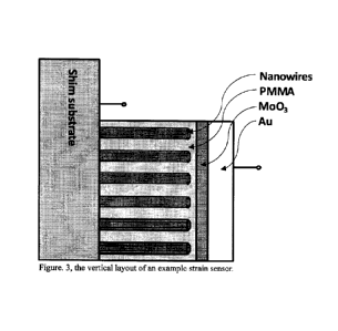
[0029] Figure 3 illustrates a preferred embodiment of the layout of a
preferred sensor system. In
this preferred embodiment, the device consists of five layers: (i) the shim
substrate (also serving
as bottom electrode, (ii) piezoelectric nanowires (for converting mechanical
strain to electrical
potential or electrical current), (iii) a poly-methyl methacrylate (PMMA)
layer (for filling the
gaps between nanowires, providing mechanical support to nanowires and
insulating the top
electrode from the bottom electrode), (iv) a Mo03 layer and (v) a Au layer (as
top electrode).
The piezoelectric nanowires (NWs) are not particularly restricted. Preferably,
the NWs are
12
CA 2985238 2017-11-10
selected from the group consisting of InN NWs, GaN NWs, ZnO NWs and the like.
ZnO NWs
can be grown on the shim substrate by using either electrochemical or
thermochemical
deposition approaches.
[0030] The ZnO NWs can be grown using electrochemical deposition in a three-
electrode
configuration, with a platinum mesh counter electrode and an Ag/AgC1 reference
electrode. An
aluminum-doped ZnO (AZO, 2 wt.% A1203 + 98 wt.% ZnO) layer was coated onto a
pre-cleaned
shim substrate using radio-frequency (RF) magnetron sputtering at 150 C. The
AZO layer
serves as both the conductive electrode and seed layer for NW growth in the
subsequent
electrochemical deposition. Photolithography was then employed to open an
array of square
windows, 200 gm apart, in a photoresist layer spun onto the AZO-coated PEN
substrate. The
retained photoresist mask ensures that NWs grow only on the exposed seed layer
in the open
windows.
[0031] The solution for growing intrinsic NWs (n-type) comprises 25 mM zinc
nitrate
(Zn(NO3)2), 12.5 mM hexamethylenetetramine (HMTA), 5 mM polyethylenemine
(PEI), and 0.3
M ammonium hydroxide. To obtain p-type NWs (Li-doped), different
concentrations of a lithium
nitrate doping reagent can be added. These concentrations (25 mM, 50 mM, and
75 mM)
corresponded to different lithium mixture ratios (100%, 200%, and 300%,
respectively) and
produced differently Li-doped NWs. The working electrode's bias was fixed at -
0.7 V with
respect to the Ag/AgC1 reference electrode. The NW length (-4 gm) was simply
controlled by
setting the growth time to 3 hours for the intrinsic section (n-type)
immediately followed by
another 3 hours for the Li-doped section (p-type). The solution temperature
was maintained at 90
C for 10 minutes followed by 88 C for 170 minutes in both cases.
[0032] Figure 4 illustrates scanning electron microscopy (SEM) images of the
ZnO NWs grown
by using the electrochemical deposition. The single-crystalline NWs are
roughly aligned along
the vertical direction having tilting angles within 250. Their diameters
range from 100 nm to
200 nm, with an area density about 2.0 x109 cm-2.
[0033] Figure 5 shows a preferred embodiment of a schematic of processing
steps of fabricating
a preferred embodiment of the present sensing system (in this case, a NW based
strain sensor).
13
CA 2985238 2017-11-10
Square- or different-shape NW patterns with a side length of 1 -10 cm can be
employed in device
fabrication. The NWs is first encapsulated with a spin-coated insulating layer
of PMMA, then
cured at 120 C for 3 hours. This layer provides a polymer matrix to protect
NWs against
damage during NG operation and prevents electrical shortage between the NGs'
top and the
bottom electrodes. Due to its flexibility, PMMA does not impede the
application of external
strain to the NWs.
[0034] To increase the interfacial energy barrier and suppress leakage
current, a thin
molybdenum oxide (Mo03) interlayer is deposited on top of the PMMA layer by
vacuum
thermal evaporation using a shadow mask, followed by the deposition of a
metallic cathode
(aluminum or gold) to complete fabrication. The devices can be packaged in
polydimethylsiloxane (PDMS), Dow Corning SylgardTM 184 premixed with curing
agent at a
ratio of 10:1 w/w and degassed, to prevent contamination, damage, and moisture
penetration
from the ambient environment.
[0035] Figure 6 illustrates a schematic layout of a preferred embodiment of
the present sensing
system based on ZnO homojunction NWs. By using ZnO homojunction NWs, the
efficiency of
converting mechanical energy to electrical energy can be significantly
enhanced. The fabrication
of such an energy harvest device is similar to that of a ZnO NW-based strain
sensor. The
difference of these two devices lies in that the strain sensor should be very
sensitive to
mechanical strain and has a very low noise level, while the energy harvester
should have a very
high efficiency in converting mechanical energy to electrical energy. The ZnO
Nanowires and
the device configurations cab be optimized differently for these two devices
in terms of their
different technical requirements.
[0036] Further details on a preferred piezoelectric nanogenerator that may be
used in a preferred
embodiment of the present sensing system may be found in copending Canadian
patent
application 2,967,004 and United States provisional patent application S.N.
62/602,895, both
filed on May 11, 2017. See, also, G. Liu, E. Abdel-Rahman, D. Ban, Performance
optimization
of p-n homoj unction nanowire-based piezoelectric nanogenerators through
control of doping
concentration. I AppL Phys., 2915, 118, 094307.
14
CA 2985238 2017-11-10
[0037] When the piezoelectric nanogenerator is InN nanowire-based, see also,
G. Liu, S. Zhao,
R. D. Henderson, Z. Leonenko, E. Abdel-Rahman, Z. Mi, and D. Ban,
"Nanogenerators based on
vertically aligned InN nanowires," Nanoscale, 2016, 8, 2097-2106.
[0038] The energy harvester unit can be also fabricated by using triboelectric
devices. The
energy conversion efficiency of a triboelectric devices typically depends on
relative mechanical
displacement of the two electrodes of the device. In a circumstance that the
mechanical relative
displacement is sizeable, a triboelectric energy harvester can be more
beneficial than a
piezoelectric energy harvester.
[0039] A triboelectric device has a simpler layer structure than a
piezoelectric device. It typically
consists of two metallic electrode layers separated by a polymer insulating
layer. Figure 7
illustrates a preferred embodiment of a triboelectric device use in the
present sensing system, the
triboelectric device comprising an upper PMMA layer, an upper electrode, a
Polydimethylsiloxane (PDMS) layer, a lower electrode and a lower PMMA layer.
The metallic
electrode can be deposited to the PMMA substrate by thermal evaporation. The
PDMS layer can
be deposited to the metallic electrode layer by spin-coating. Metallic
nanoparticles (such as Au
nanoparticles) can be inserted to the interface between the PDMS layer and the
lower electrode
layer to enhance the energy conversion efficiency.
[0040] In a preferred embodiment, the triboelectric nanogenerator for use in
the present sensing
system is produced using the following non-limiting process:
1. A mold layer will be patterned using photolithography on a silicon wafer (5
inches in diameter, for example).
2. The patterned wafers will be etched anisotropically using a dry etching
process, resulting in the formation of recessed pyramids.
3. After cleaned with acetone and isopropanol, all of the Si wafers were
treated
with trimethylchlorosilane (Sigma Aldrich) by gas phase silanization to avoid
the adhesion between PDMS and Si molds.
CA 2985238 2017-11-10
4. In preparing the patterned polymer films, PDMS elastomer and cross-linker
(Sylgard 184, Tow Corning) will be mixed, and then casted on the Si wafer.
5. After a degassed process under vacuum, the elastomer mixture will be spin-
coated at 500 rpm for 60 s.
6. After incubated at 85 C for 1 h, a uniform PDMS thin film was peeled off
from Si mold and then placed on uncured PDMS on a piece of clean ITO-
coated PET film.
7. Finally, another clean ITO- coated PET film will be placed onto the
prepared
PDMS-PET substrate to form a sandwiched structure.
8. The two short edges of the device will be sealed with ordinary adhesive
tape
to ensure an adequate contact between PET and patterned PDMS films.
[0041] As many shim substrates are made of metallic materials, they can be
used as the upper
and lower electrode layers, which can simplify the device fabrication and
integration of the
energy harvester component in the present sensing system.
[0042] The generated energy is preferably stored in a battery or capacitor so
that it can be used
to power devices in a regulated manner. Between the power generation unit and
a storage unit, it
is preferred to implement a power management circuit to maximize power storage
efficiency.
The central goal is to develop more-efficient energy harvesting and management
circuitry for
transferring harvested energy to the battery layers for storage, as well as
for managing the energy
consumed by the data unit.
[0043] Figure 8 illustrates a preferred embodiment of the basic layout of an
example power unit,
which typically includes an electronic circuit for converting AC electrical
current to DC
electrical current and an energy storage unit. The AC electrical power from
the energy harvester
is converted to DC electrical power via the AC to DC converter and is stored
in the energy
storage unit. The stored electrical power will be used to bias the other
components (such as the
data unit) for strain data collection and transmission.
16
CA 2985238 2017-11-10
[0044] A representative AC to DC converter circuit is shown in Figure 9, which
consists of four
pn junction diode and one capacitor. The pn junctions and the capacitor can be
fabricated by
using ASIC (amorphous silicon integration circuit) technologies. The energy
storage unit can be
a super-capacitor or thin-film based lithium rechargeable batteries. For
metallic shim substrates,
two neighboring shim layers separated by an electrical insulating layer with a
high dielectric
constant can be used as the two electrodes of the super-capacitor.
[0045] The data unit is for strain signal collection and transmission. The
data unit can be a
standalone unit, which is commercially-available, such as RF24L01 wireless
connector from
Soc-Robotics.com. It can transmit the collected strain signal to a base
station that is in a short
distance. Another option is to directly fabricate a data collection and
transmission circuit on a
shim substrate by using ASIC technologies. As the wireless transmission
distance is short and
the data transmission rate is low, such an ASIC circuit should be sufficient
to meet the technical
requirements of the data unit.
[0046] Figure 10 illustrates the preliminary experimental results of a ZnO
nanowire based
piezoelectric energy harvester fabricated on a flexible substrate. The average
peak open-circuit
voltage is 0.7 V and the average peak short-circuit current is 42 nA, yielding
a 0.03 IAW peak
output power.
[0047] Figure 11 illustrates a demonstration of a proof-of-concept setup for
wireless strain signal
transmission. The strain sensors are two commercial strain gauges (Vishay
precision group),
which are under mechanical vibration. The strain data was then collected by a
wireless sensor
node powered by an energy harvesting system and transmitted to a nearby base
station. The
preliminary experimental results show that the applied strain on the strain
sensors was measured
to be 1600 I-LE at a frequency of 3 Hz.
[0048] While this invention has been described with reference to illustrative
embodiments and
examples, the description is not intended to be construed in a limiting sense.
Thus, various
modifications of the illustrative embodiments, as well as other embodiments of
the invention,
will be apparent to persons skilled in the art upon reference to this
description. It is therefore
contemplated that the appended claims will cover any such modifications or
embodiments.
17
CA 2985238 2017-11-10
[0049] All publications, patents and patent applications referred to herein
are incorporated by
reference in their entirety to the same extent as if each individual
publication, patent or patent
application was specifically and individually indicated to be incorporated by
reference in its
entirety.
18
CA 2985238 2017-11-10
LIST OF BACKGROUND REFERENCES
[1] G. Liu, "Semiconductor Nanowire Based Piezoelectric Energy Harvesters:
Modeling,
Fabrication, and Characterization," Ph.D. thesis, 2015, University of
Waterloo.
[2] M. Q. Le, J.-F. Capsal, M. Lallart, Y. Hebrard, A. Van Der Ham, N. Reffe,
L. Geynet, and
P.-J. Cottinet, "Review on energy harvesting for structural health monitoring
in aeronautical
applications," Prog. Aerosp. Sci., 2015, 79, 147-157.
[3] Y. Hu and Z. L. Wang, "Recent progress in piezoelectric nanogenerators as
a sustainable
power source in self-powered systems and active sensors," Nano Energy, 2015,
14, 3-14.
[4] R. Hinchet, W. Seung, and S. W. Kim, "Recent Progress on Flexible
Triboelectric
Nanogenerators for SelfPowered Electronics," ChemSusChem, 2015, 8, 2327-2344.
[5] F. R. Fan, W. Tang, and Z. L. Wang, "Flexible Nanogenerators for Energy
Harvesting and
Self-Powered Electronics," Adv. Mater., 2016.
[6] Z. L. Wang, J. Chen, and L. Lin, "Progress in triboelectric nanogenerators
as a new energy
technology and self-powered sensors," Energy Environ. Sci., 2015, 8, 2250-
2282.
[7] J. Briscoe and S. Dunn, "Piezoelectric nanogenerators¨a review of
nanostructured
piezoelectric energy harvesters," Nano Energy, 2015, 14, 15-29.
[8] S. Wang, L. Lin, and Z. L. Wang, "Triboelectric nanogenerators as self-
powered active
sensors," Nano Energy, 2015, 11, 436-462.
[9] M. Han, X.-S. Zhang, B. Meng, W. Liu, W. Tang, X. Sun, W. Wang, and H.
Zhang, "r-
Shaped hybrid nanogenerator with enhanced piezoelectricity," ACS Nano, 2013,
7, 8554-
8560.
[10] X. Li, Z.-H. Lin, G. Cheng, X. Wen, Y. Liu, S. Niu, and Z. L. Wang, "3D
Fiber-Based
Hybrid Nanogenerator for Energy Harvesting and as a Self-Powered Pressure
Sensor," ACS
Nano, 2014, 8, 10674-10681.
19
CA 2985238 2017-11-10
[11] K. Y. Lee, M. K. Gupta, and S.-W. Kim, "Transparent flexible stretchable
piezoelectric and
triboelectric nanogenerators for powering portable electronics," Nano Energy,
2015, 14,
139-160.
[12] S.-B. Jeon, D. Kim, G.-W. Yoon, J.-B. Yoon, and Y.-K. Choi, "Self-
cleaning hybrid energy
harvester to generate power from raindrop and sunlight," Nano Energy, 2015,
12, 636-645.
[13] X. Wang, S. Wang, Y. Yang, and Z. L. Wang, "Hybridized
Electromagnetic¨Triboelectric
Nanogenerator for Scavenging Air-Flow Energy to Sustainably Power Temperature
Sensors," ACS Nano, 2015, 9, 4553-4562.
[14] T. Quan, X. Wang, Z. L. Wang, and Y. Yang, "Hybridized
Electromagnetic¨Triboelectric
Nanogenerator for a Self-Powered Electronic Watch," ACS Nano, 2015, 9, 12301-
12310.
[15] Y. Zi, L. Lin, J. Wang, S. Wang, J. Chen, X. Fan, P. K. Yang, F. Yi, and
Z. L. Wang,
" Tribo el ectric¨P yroel ectric¨P iezoelectric Hybrid Cell
for High-Efficiency
Energy-Harvesting and Self-Powered Sensing," Adv. Mater., 2015, 27, 2340-2347.
[16] Y. Yang and Z. L. Wang, "Hybrid energy cells for simultaneously
harvesting multi-types of
energies," Nano Energy, 2015, 14, 245-256.
[17] S. Wang, Z. L. Wang, and Y. Yang, "A One-Structure-Based Hybridized
Nanogenerator for
Scavenging Mechanical and Thermal Energies by Triboelectric-Piezoelectric-
Pyroelectric
Effects," Advanced materials (Deerfield Beach, Fla.), 2016.
[18] W.-S. Jung, M.-G. Kang, H. G. Moon, S.-H. Baek, S.-J. Yoon, Z.-L. Wang,
S.-W. Kim, and
C.-Y. Kang, "High output piezo/triboelectric hybrid generator," Sci. Rep.,
2015, 5.
[19] S. Niu, Y. Liu, S. Wang, L. Lin, Y. S. Zhou, Y. Hu, and Z. L. Wang,
"Theoretical
Investigation and Structural Optimization of Single-Electrode Triboelectric
Nanogenerators," Adv. Funct. Mater., 2014, 24, 3332-3340.
[20] H. Jang, Y. J. Park, X. Chen, T. Das, M. S. Kim, and J. H. Ahn, "Graphene-
Based Flexible
and Stretchable Electronics," Adv. Mater., 2016.
CA 2985238 2017-11-10
[21] C. Hu, L. Song, Z. Zhang, N. Chen, Z. Feng, and L. Qu, "Tailored graphene
systems for
unconventional applications in energy conversion and storage devices," Energy
Environ.
Sci., 2015, 8, 31-54.
[22] B. N. Chandrashekar, B. Deng, A. S. Smitha, Y. Chen, C. Tan, H. Zhang, H.
Peng, and Z.
Liu, "Roll-to-Roll Green Transfer of CVD Graphene onto Plastic for a
Transparent and
Flexible Triboelectric Nanogenerator," Adv. Mater., 2015, 27, 5210-5216.
[23] S. Kim, M. K. Gupta, K. Y. Lee, A. Sohn, T. Y. Kim, K. S. Shin, D. Kim,
S. K. Kim, K. H.
Lee, and H. J. Shin, "Transparent flexible graphene triboelectric
nanogenerators," Adv.
Mater., 2014, 26, 3918-3925.
[24] L. E. Greene, M. Law, J. Goldberger, F. Kim, J. C. Johnson, Y. Zhang, R.
J. Saykally, and
P. Yang, "Low-temperature wafer-scale production of ZnO nanowire arrays,"
Angew. Chem.
mt. Ed, 2003, 42, 3031-3034.
[25] D.-M. Shin, E. L. Tsege, S. H. Kang, W. Seung, S.-W. Kim, H. K. Kim, S.
W. Hong, and
Y.-H. Hwang, "Freestanding ZnO nanorod/graphene/ZnO nanorod epitaxial double
heterostructure for improved piezoelectric nanogenerators," Nano Energy, 2015,
12, 268-
277.
[26] G. Liu, S. Zhao, R. D. Henderson, Z. Leonenko, E. Abdel-Rahman, Z. Mi,
and D. Ban,
"Nanogenerators based on vertically aligned InN nanowires," Nanoscale, 2016,
8, 2097-
2106.
[27]G. Liu, E. Abdel-Rahman, D. Ban, Performance optimization of p-n
homojunction
nanowire-based piezoelectric nanogenerators through control of doping
concentration. I
AppL Phys., 2915, 118, 094307.
[28] R. S. Dhar, L. Li, H. Ye, S, G. Razavipour, X. Wang, R. Q. Yang, D. Ban,
"Nanoscopically
resolved dynamic charge carrier distribution in operating interband cascade
lasers," Laser &
Photonics Review, 2015, 8, 224.
[29] R. S. Dhar, S. G. Razavipour, E. Dupont, C. Xu, S. Laframboise, Z.
Wasilewski, Q. Hu, D.
21
CA 2985238 2017-11-10
Ban, " Direct Nanoscale Imaging of Evolving Electric Field Domains in Quantum
Structures," Scientific Reports, 2014, 4, 7183.
[30] S. Fathololoumi, E. Dupont, C. W. I. Chan, etc., "Terahertz quantum
cascade lasers
operating up to ¨200K with optimized oscillator strength and improved
injection tunneling,"
Optics Express, 2012, 20, 3866.
[31] Jun Chen, Dayan Ban, Michael G. Helander, Zhenghong Lu and P. Poole,
"Near-infrared
inorganic/organic optical upconverter with an external efficiency of > 100%",
Advanced
Materials, 2010, 22, 4900.
[32]Jun Chen, Jianchen Tao, Dayan Ban, M. G. Helander, Z. Wang, J. Qiu, Z. H.
Lu,
"Organic/Inorganic Hybrid Pixelless Imaging Device," Advanced Materials, 2012,
24, 3138.
[33]Cheng-Ying Chen, Jun-Han Huang, Jinhui Song, Yusheng Zhou, Long Lin, Po-
Chien
Huang, Yan Zhang, Chuan-Pu Liu, Jr-Hau He, and Zhong Lin Wang, "Anisotropic
Outputs
of a Nanogenerator from Oblique-Aligned ZnO Nanowire Arrays" ACS Nano, 2011,
5,
6707-6713.
[34] Nai-Jen Ku, Jun-Han Huang, Chao-Hung Wang, Hsin-Chiao Fang, and Chuan-Pu
Liu,
"Crystal Face-Dependent Nanopiezotronics of an Obliquely Aligned InN Nanorod
Array"
Nano Letters, 2012, 12, 562-568.
[35] Ruey-Chi Wang, Hsin-Ying Lin, Chao-Hung Wang, and Chuan-Pu Liu,
"Fabrication of a
large-area Al-doped ZnO nanowire array photosensor with enhanced photoresponse
by
straining" Advanced Functional Materials, 2012, 22, 3875-3881.
[36] Nai-Jen Ku, Chao-Hung Wang, Jun-Han Huang, Hsin-Chiao Fang, Po-Chien
Huang and
Chuan-Pu Liu, "Energy Harvesting from the Obliquely Aligned InN Nanowire Array
with a
Surface Electron-Accumulation Layer" Advanced Materials, 2013, 25, 861-866.
[37] Chia-Hao Tu, Waileong Chen, Hsin-Chiao Fang, Yonhua Tzeng, Chuan-Pu Liu,
"Heteroepitaxial nucleation and growth of graphene nanowalls on silicon"
Carbon, 2013, 54,
234-240.
22
CA 2985238 2017-11-10
[38] Chao-Hung Wang, Wei-Shun Liao, Zong-Hong Lin, Nai-Jen Ku, Yi-Chang Li,
Yen-Chih
Chen, Zhong-Lin Wang and Chuan-Pu Liu, "Optimization of the Output Efficiency
of GaN
Nanowire Piezoelectric Nanogenerators by Tuning the Free Carrier
Concentration"
Advanced Energy Materials, 2014, 4, 1400392.
[39] Chao-Hung Wang, Wei-Shun Liao, Nai-Jen Ku, Yi-Chang Li, Yen-Chih Chen, Li-
Wei Tu
and Chuan-Pu Liu, "Effects of Free Carriers on Piezoelectric Nanogenerators
and
Piezotronic Devices Made of GaN Nanowire Arrays" Small, 2014, 10, 4718-4725.
[40] Yen-Yu Chen, Chao-Hung Wang, Giin-Shan Chen, Yi-Chang Li and Chuan-Pu
Liu, "Self-
powered n-MgxZn1 -x0/p-Si photodetector improved by alloying-enhanced
piezopotential
through piezo-phototronic effect" Nano Energy, 2015, 11, 533-539.
[41] Chao-Hung Wang, Kun-Yu Lai, Yi-Chang Li, Yen-Chih Chen, and Chuan-Pu Liu,
"Ultrasensitive Thin-Film-Based AlxGai-xN Piezotronic Strain Sensors via
Alloying-
Enhanced Piezoelectric Potential" Advanced Materials, 2015, 27, 6289-6295.
[42] Dayan Ban, Guocheng Liu, Cascade-type hybrid energy cells for driving
wireless sensors,
copending Canadian patent application 2,967,004 and United States provisional
patent
application S.N. 62/602,895, both filed on May 11, 2017.
23
CA 2985238 2017-11-10