Note: Descriptions are shown in the official language in which they were submitted.
CA 02985701 2017-11-10
WO 2016/184982 PCT/EP2016/061324
PACKAGING LABEL AND METHOD FOR LABELLING A PACKAGE
The present invention relates to a packaging label and to a method for
labelling a
package.
In the packaging industry labels with fixed graphics are known, i.e. bearing a
predetermined message, which may be adhesive or printed directly onto the
packaging,
for example a plastic or glass bottle.
However, such labels have the disadvantage of being able to produce only one
message
(e.g. product name, list of ingredients, promotional message), therefore for
many
commercial products, it is necessary to use a plurality of different labels,
each dedicated
to specific contents.
In the field of electronics on plastic, dynamic labels are also known,
provided with a
display for displaying a plurality of different messages, such as, for
example, a
promotional message, the expiry date and/or the ingredients of the packaged
product.
However, such labels are not fully comprised of materials compatible with
recycling
(including the display) and the production process is not compatible with high
performance printing or with direct printing on the packaging container.
Furthermore,
such labels must be self-supplied and not even the supply unit satisfies the
above
indicated requirements.
Therefore, there is a need to find innovative solutions to the problem of
"dynamically"
labelling packaged products, mainly for marketing and advertising purposes.
The object of the invention is therefore to propose a dynamic label able to
progressively
change the contents displayed, which may be directly printed and/or integrated
onto the
packaging and which is compatible with current packaging production processes,
by
adding to the packaging itself a negligible cost in order to be economically
sustainable.
CA 02985701 2017-11-10
WO 2016/184982
PCT/EP2016/061324
A further object of the invention is that of proposing an easily recyclable
label.
These and other objects are reached with a label whose characteristics are
defined in
claim 1.
Particular embodiments form the subject matter of the dependent claims, whose
contents
are to be considered an integral part of the present description.
Further characteristics and advantages of the invention will appear from the
following
detailed description, given by way of non-limitative example, with reference
to the
appended drawings, in which:
- Figure 1 is a schematic front view of a label according to the present
invention;
- Figure 2 illustrates a front view of an embodiment of the label of Figure
1;
- Figure 3 shows a sectional view of the label of Figure 1;
- Figure 4 shows a variation of the label according to the present
invention; and
- Figure 5 shows a block diagram of the operations of the method for
obtaining a
label according to the present invention.
In summary, a label according to the present invention is fully recyclable,
can be printed
with high performance printing processes either on plastic or on paper or
directly on
plastic packaging, for example PET, and can be used with the current packaging
industry
standards. The label according to the present invention also integrates a
source of
independent energy.
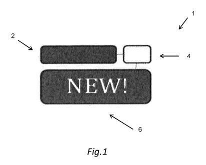
Figure 1 shows a schematic front view of a label 1 according to the present
invention.
Such label 1 comprises at least a photovoltaic source 2 adapted to supply a
control
module 4 and a display 6 bearing a message.
The photovoltaic source 2 is a photovoltaic module known in itself, which
preferably uses
a bulk heterojunction organic technology. Alternatively, the photovoltaic
source is not
organic, being, for example, a photovoltaic source based on quantum dots or
hybrid
2
CA 02985701 2017-11-10
WO 2016/184982
PCT/EP2016/061324
perovskite. The photovoltaic module 2 can be printed, in a known way, on a
plastic
substrate, for example, polyethylene terephthalate (PET) having a thickness
preferably
comprised in the interval 1pm - 100 pm.
Figure 2 shows a front view of an embodiment of the label 1 in which there are
a plurality
of photovoltaic modules 2 arranged along a circumference, the display 6
corresponding to
the area containing the message and the control module 4 being next to the
display 6
(alternatively, the control module 4 is positioned below the display 6 as
described in detail
below).
Below, with reference to figures 3 and 4, the process will be described for
obtaining a
label according to the present invention, the block diagram of which is shown
in figure 5.
Such a procedure starts with a first step 100 of providing a substrate 10,
preferably of the
type described above. Such substrate 10 may be transparent or opaque. In an
embodiment of the present invention, the label is printed directly on the
packaging (e.g. a
plastic bottle or paper box), in which case the substrate is the surface of
the packaging
itself. Alternatively the substrate could be made of (or including) other
materials, e.g.
metal foils, rubber, self-adhesive substrate, tattoo paper.
Figure 3 shows a sectional view of the label 1 in which the substrate 10 is
present,
preferably a plastic sheet or bottle, onto which, in step 102 the photovoltaic
module is
printed. Between the photovoltaic modules 2 in steps 104 and 106 the control
module 4,
preferably comprising at least a low power supply thin film transistor, and
the display 6
are printed, respectively, the latter preferably provided in the form of a
layer of electrically
addressable material, e.g. and electrochromic material. Alternatively the
layer could be
made of any other electrically addressable material, e.g. electroluminescent
material.
A fundamental limit connected with organic electronic printing (steps 102 -
106 described
above) on thin (10-200 pm) and ultrathin (less than 10 pm) plastic supports is
connected
3
CA 02985701 2017-11-10
WO 2016/184982
PCT/EP2016/061324
with the maximum temperature of the printing process. Typically, to perform
such printing,
thermal heating processes are required, which are not compatible with the thin
layer of
plastic substrate used in the packaging, since such a layer would be heat
sensitive. The
optimisation of the organic electronic printing process is closely connected
with the
annealing processes, which typically require temperatures of over 100 C,
necessary for
optimising the performance of the printed devices, for example, improving the
mobility of
charge carriers, de-absorbing contaminants and obtaining the desired
morphology of the
support layer.
In the printing operations 102-106 described above, ink is used which is in
itself known, to
which, before performing the printing itself, dopants are added, preferably
precursors of
benzimidazole and benzimidazoline or caesium or lithium salts.
Thanks to the use of these particular chemical dopants, optimised electronics
are
obtained, printed directly at room temperature or however at low temperatures
compatible
with the substrate 10 (preferably lower than 70 C), in which only the
evaporation of the
ink solvent is required.
The control module 4 is provided to send control signals to the display 6 so
that
predetermined messages are shown on the display 6.
The control module 4 and the display 6 are in electrical contact with the
photovoltaic
module 2 for allowing its supply by the latter.
Above the control module 4 and the display 6, in step 108, an electrical
lateral
interconnecting layer 12 is deposited, preferably of ion-gel or solid
electrolyte type, which
allows the control module 4 to perform a low voltage control of the display 6,
i.e. allowing
the control module 4 to send control signals to the display 6.
Alternatively, the control module 4 is provided through at least one thin film
transistor
comprising semiconductor metal oxides such as, for example, ZnO, IZO, IGZO.
4
CA 02985701 2017-11-10
WO 2016/184982
PCT/EP2016/061324
Finally, in step 110, on top of all the underlying layers, a barrier layer 14
is deposited,
preferably oxide/polymer multilayer, for example silica and alumina for the
inorganic layer
and EVA, ETFE, PET or PEN for the organic layer, so as to protect the
underlying layers
from oxygen and water vapour.
Figure 4 shows a variation of the invention wherein similar layers are
indicated with the
same reference numbers. In this variation, only the display 6 is placed
between two
photovoltaic modules 2 above the substrate 10 and not also the control module
4. Above
the photovoltaic modules 2 and the display 6 an insulating layer 16 is first
deposited,
having a predetermined pattern, i.e. a plurality of holes 16a placed in
correspondence of
the display 6 and subsequently the control module 4 is deposited which,
through the
holes 16a, comes into contact with the display 6 below. Finally, above the
control module
4 the barrier layer 14 is deposited.
Therefore, in this embodiment, during use, there will be the front display 6
and the control
module 4 behind it.
The label 1 according to the present invention is recyclable because all the
electronic
components are made with plastic electronic materials or easily separable from
plastic
(metallisations of silver or other metals).
The active label 1 is also recyclable because the materials of which each of
its
components are comprised, i.e. the photovoltaic module 2, the control module 4
and the
display 6 are characterised by a low melting temperature (comprised between
200 and
400 C). In this way, any traces of non-plastic materials (metals, metal
oxides, etc.)
present in the label 1 can be removed by filtering, in a known way, through
techniques for
the purification of recycled plastic.
Naturally, various modifications to the principle of the invention, the
embodiments and
construction details may be possible, according to what is described and
disclosed
CA 02985701 2017-11-10
WO 2016/184982
PCT/EP2016/061324
merely by way of non-limitative example, without departing from the scope of
the present
invention, as defined by the appended claims.
6