Note: Descriptions are shown in the official language in which they were submitted.
THREE-PHASE TIIREE-LEVEL INVERTER WITH REDUCED COMMON MODE
LEAKAGE CURRENT
FIELD
[0001] Embodiments described herein relate generally to power
conversion, and
specifically to a three-phase three-level inverter with reduced common mode
leakage
current.
BACKGROUND
[0002] Power inverters include circuitry that functions to change
direct current
(DC) power to alternating current (AC) power. The size, configuration, and
control of
an inverter may depend on its application. For instance, in a large-scale
power system
with an AC power grid, a three-phase inverter is typically used to connect a
DC power
source, such as one or more photovoltaic (PV) panels, to the power grid. In
those
applications, an oftentimes heavy and expensive transformer is typically used
to isolate
the PV panel from the AC power source. Removing the transformer may be
beneficial in
that it reduces the size and expense of the power system, but the lack of
isolation can
cause a common mode leakage current to form, which can degrade the current
provided
by the inverter to the power grid or improperly trigger ground fault
protection. Similar
leakage currents generated at inverters used in other applications can have
the same
deleterious effects. Different types of inverters may be used to make this
connection,
including, but not limited to, neutral-point-clamped (NPC) inverters, flying
capacitor
inverters, and cascaded H-bridge inverters. Each type of inverter may have
benefits and
drawbacks. For instance, NPC inverters typically have the fewest number of
components and can use less expensive components with lower voltage ratings.
NPC
inverters, however, can experience voltage imbalance problems that can
increase the
total harmonic distortion (THD) in the output signal. NPC and other types of
inverters
1
CA 2985751 2017-11-15
may also suffer from leakage current that can further degrade the output
signal.
BRIEF DESCRIPTION OF THE DRAWINGS
[0003] Some specific exemplary embodiments of the disclosure may be
understood by referring, in part, to the following description and the
accompanying
drawings.
[0004] Figures 1A-B illustrate an example power system, according to
aspects
of the present disclosure.
[0005] Figure 2 is a diagram illustrating an example space vector
diagram for
space vector modulation, according to aspects of the present disclosure.
[0006] Figures 3A-B through 6A-B are diagrams illustrating an example
modulation scheme, according to aspects of the present disclosure.
[0007] Figures 7-9 illustrate an example substitution of a non-adjacent
small
vector for an adjacent small vector to create a complementary pair of
sequences
applicable by the controller to balance the common mode voltage, according to
aspects
of the present disclosure.
[0008] Figures 10A-C illustrate simulated results of grid current,
common mode
voltage, and leakage current of a three-phase three-level inverter system,
wherein the
controller applies known sequences of switching states according to aspects of
the
present disclosure.
[0009] Figures 11A-C illustrate simulated results of grid current,
common mode
voltage, and leakage current of a three-phase three-level inverter system,
wherein the
controller applies sequences comprising reduced common mode voltage switching
states, according to aspects of the present disclosure.
[0010] Figures 12A-C illustrate simulated results of grid current,
common mode
voltage, and voltages across two capacitors of a three-phase three-level
inverter system,
2
CA 2985751 2017-11-15
wherein the controller applies active voltage balancing across the two
capacitors
according to aspects of the present disclosure.
[0011] Figures 13A-D through Figures 36A-D illustrate active-high and
active-low complementary P- and N-type sequences associated with the 24
sectors
illustrated in Figure 2, according to aspects of the present disclosure.
[0012] While embodiments of this disclosure have been depicted and
described
and are defined by reference to exemplary embodiments of the disclosure, such
references do not imply a limitation on the disclosure, and no such limitation
is to be
inferred. The subject matter disclosed is capable of considerable
modification, alteration,
and equivalents in form and function, as will occur to those skilled in the
pertinent art
and having the benefit of this disclosure. The depicted and described
embodiments of
this disclosure are examples only, and not exhaustive of the scope of the
disclosure.
3
CA 2985751 2017-11-15
DETAILED DESCRIPTION
[0013] Embodiments described herein relate generally to power systems
thereof,
and specifically to a three-phase three-level inverter with reduced common
mode
leakage current and active balance control.
[0014] For purposes of this disclosure, an information handling system
may
include any instrumentality or aggregate of instrumentalities operable to
compute,
classify, process, transmit, receive, retrieve, originate, switch, store,
display, manifest,
detect, record, reproduce, handle, or utilize any form of information,
intelligence, or
data for business, scientific, control, or other purposes. For example, an
information
handling system may be a personal computer, a network storage device, or any
other
suitable device and may vary in size, shape, performance, functionality, and
price. The
information handling system may include random access memory (RAM), one or
more
processing resources such as a central processing unit (CPU) or hardware or
software
control logic, ROM, and/or other types of nonvolatile memory. Additional
components
of the information handling system may include one or more disk drives, one or
more
network ports for communication with external devices as well as various input
and
output (I/O) devices, such as a keyboard, a mouse, and a video display. The
information
handling system may also include one or more buses operable to transmit
communications between the various hardware components. It may also include
one or
more interface units capable of transmitting one or more signals to a
controller, actuator,
or like device.
[0015] For the purposes of this disclosure, computer-readable media may
include any instrumentality or aggregation of instrumentalities that may
retain data
and/or instructions for a period of time. Computer-readable media may include,
for
example, without limitation, storage media such as a direct access storage
device (e.g., a
hard disk drive or floppy disk drive), a sequential access storage device
(e.g., a tape disk
4
CA 2985751 2017-11-15
drive), compact disk, CD-ROM, DVD, RAM, ROM, electrically erasable
programmable read-only memory (EEPROM), and/or flash memory; as well as
communications media such wires, optical fibers, microwaves, radio waves, and
other
electromagnetic and/or optical carriers; and/or any combination of the
foregoing.
[0016] Illustrative embodiments of the present disclosure are described
in detail
herein. In the interest of clarity, not all features of an actual
implementation may be
described in this specification. It will of course be appreciated that in the
development
of any such actual embodiment, numerous implementation specific decisions are
made
to achieve the specific implementation goals, which will vary from one
implementation
to another. Moreover, it will be appreciated that such a development effort
might be
complex and time-consuming, but would nevertheless be a routine undertaking
for those
of ordinary skill in the art having the benefit of the present disclosure.
[0017] The terms "couple" or "couples" as used herein are intended to
mean
either an indirect or a direct connection. Thus, if a first device couples to
a second
device, that connection may be through a direct connection or through an
indirect
mechanical or electrical connection via other devices and connections.
Similarly, the
term "communicatively coupled" as used herein is intended to mean either a
direct or an
indirect communication connection. Such connection may be a wired or wireless
connection such as, for example, Ethernet, local area network (LAN), radio
frequency,
power-line communication (PLC), or other communication means that would be
appreciated by one of ordinary skill in the art in view of this disclosure.
Thus, if a first
device communicatively couples to a second device, that connection may be
through a
direct connection, or through an indirect communication connection via other
devices
and connections.
[0018] Hereinafter, embodiments will be described with reference to the
drawings. Each drawing is a schematic view for describing an embodiment of the
CA 2985751 2017-11-15
present disclosure and promoting the understanding thereof. The drawings
should not be
seen as limiting the scope of the disclosure. In each drawing, although there
are parts
differing in shape, dimension, ratio, and so on from those of an actual
apparatus, these
parts may be suitably changed in design taking the following descriptions and
well-known techniques into account.
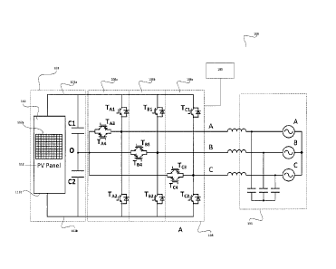
[0019] Figs. 1A and 1B diagram an example power system 100 comprising a
DC connection 102, a three-phase AC connection 104, and a three-phase three-
level
inverter 106 that includes three phases 106a, 106b, and 106c of switches for
coupling
the DC connection 102 and the three-phase AC connection 104. The DC connection
102
comprises first and second DC terminals 102a and 102b for receiving power from
a DC
source 110, as well as first and second DC bus capacitors Cl and C2 coupled in
series
between the terminals 102a/102b. The capacitors Cl and C2 may be coupled
together at
a common node or the neutral point 0. The voltage across the terminals 102a
and 102b
may be referred to as a DC bus voltage, V pc, with the terminal 102a
comprising a
positive terminal and the terminal 102b comprising a negative terminal. The
capacitors
Cl and C2 may have substantially the same capacitance and voltage ratings,
such that
the neutral point 0 is ideally at a voltage half way between the voltages at
the DC
terminals 102a and 102b.
[0020] As depicted, the DC source 110 comprises a PV panel 112 that
includes
one or more PV cells 112a and a frame 112b. Although only one PV panel 112 is
depicted, the DC source 110 may comprise a plurality of PV panels or other PV
elements than generate DC power. The DC source 110 may also comprise any other
DC
sources that would be appreciated by one of ordinary skill in the art in view
of this
disclosure, including, but not limited to batteries.
[0021] The AC connection 104 comprises three input terminals A, B, and
C that
are respectively coupled to output terminals of the phases 106a, 106b, and
106c of the
6
CA 2985751 2017-11-15
inverter 106. These A, B, and C terminals may be connected, for instance, to a
Y-connected three-phase load (not shown) at the AC connection 104, or to any
other
multi-phase implementation that would be appreciated by one of ordinary skill
in the art
in view of this disclosure. In certain embodiments, the AC connection 104 may
comprise, for instance, a public power grid or a local power grid or system
that may
receive power from the PV panel 112 through the inverter 106 and provide AC
power to
buildings, houses, and the like. The AC power destination 104 is not limited
to power
grids, however, and may comprise any device or system that requires or uses AC
power.
[0022] The phases 106a, 106b, and 106c of the inverter 106 may comprise
respective switching devices TAI-TA4, 'FBI-T{34, and T1-Tc4 The switching
devices
TAI-TA4, 'FBI-TM, and Tc1-Tc4may comprise one or more transistors, including,
but not
limited to, bipolar junction transistors (BJTs), junction gate field-effect
transistors
(JFETs), and metal¨oxide¨semiconductor field-effect transistor (MOSFETs). As
depicted in Fig. 1A, the switching devices TAI-TA4, TBI-TB4, and Tci-Tc4 of
each phase
are arranged in a t-type configuration with respect to the DC terminals 102a
and 102b
and the neutral point 0. For instance, with respect to phase 106a, the
switching devices
TA] and TA2 are connected in series between the terminals 102a and 102b, and
the
switching devices TA, and TA4 are connected in parallel with opposite polarity
to the
neutral point 0 and a common node between the switching devices TA! and TA2,
to
which the lead A is also connected. The switching devices TB I -TB4 and Tci-
Tc4 of
phases 106b and 106c may comprise similar arrangements with respect to the
neutral
point 0, the terminals 102a/b, and the corresponding leads of the AC
connection 104.
[0023] Fig. 1B illustrates an alternative configuration, in which
switching
devices TA3 and TA4 are each configured in parallel with a diode and the
switching
device/diode pairs are arranged in series between, but with opposite
polarities to, the
neutral point 0 and a common node between the switching devices TAI and TA2,,
to
7
CA 2985751 2017-11-15
which the lead A is also connected. As in Fig. 1A, Fig. l B shows the
switching devices
TB! -1134 and Tci-TC4 of phases 106b and 106c may comprise similar
arrangements with
respect to the neutral point 0, the terminals 102a/b, and the corresponding
leads of the
AC connection 104. The switching device configurations illustrated in Figs. lA
and 1B
are not intended to be limiting, however, as other configurations are
possible.
[0024] The inverter 106 may further comprise a controller 160. The
controller
160 may comprise an information handling system with a processor and a memory
device coupled to the processor. In certain embodiments, the controller 160
may
comprise microprocessors, microcontrollers, digital signal processors (DSP),
application
specific integrated circuits (ASIC), or any other digital or analog circuitry
configured to
interpret and/or execute program instructions and/or process data. The
controller 160
may be coupled to and control the operation of the switching devices TA 1 -
TA4, TB I -TB4,
and T1-T4 For instance, the controller 160 may output individual switching
signals to
each of the switching devices TA 1 -TA4, TB I -TB4, and Tc1-Tc4 to turn the
switching
devices "on" to conduct current, or "off' to prevent current flow. In the
embodiment
depicted, where the switching devices TA I -TA4, TB I -T134, and T1-Tc4
comprise
transistors, the controller 160 may be coupled to the gates of the
transistors, and the
switching signals may comprise voltage signals applied to the gates of the
transistors.
[0025] The controller 160 may operate each of the phases 106a-c
individually in
one of three modes or levels. A first mode may be referred to as "P- and may
correspond to a configuration in which the switches of a given phase connect
the
corresponding lead of the AC connection 104 to the positive terminal 102a of
the DC
connection. With respect to the phase 106a, a P-mode may be established when
transistors TA2 and TA3 are "off' and either transistor TA1 alone is "on" or
both
transistors TA! and TA4 are "on," such that the lead A is connected to the
terminal 102a.
A second mode may be referred to as "0" and may correspond to a configuration
in
8
CA 2985751 2017-11-15
which the switches of a given phase connect the corresponding lead of the AC
connection 104 to the neutral point 0. With respect to the phase 106a, an 0-
mode may
be established when transistors TA3 and TA4 are "on" and transistors TA! and
TA2 are
"off," such that the lead A is connected to the neutral point 0. A third mode
may be
referred to as "N" and may correspond to a configuration in which the switches
of a
given phase connect the corresponding lead of the AC connection 104 to the
negative
terminal 102b of the DC connection 102. With respect to the phase 106a, an N-
mode
may be established when transistors TAI and TA4 are "off' while either
transistor TA2
alone is "on" or both transistors TA2 and TA3 are "on," such that the lead A
is connected
to the terminal 102b.
[0026] The inverter 106 may be characterized by one or more switching
states
that correspond to the combinations of modes in which the phases 106a-c are
operating
at a given time. For instance, one switching state may be referred to as "PPP"
and may
correspond to a state of the inverter 106 in which all three phases 106a-c are
operating
in the P-mode such that each lead A, B, and C of the AC connection 104 is
connected to
the terminal 102a. Another example switching state may be referred to as "PON"
and
may correspond to a state of the inverter 106 in which the first phase 106a is
operating
in the P-mode, the second phase 106b is operating in the 0-mode, and the third
phase
106c is operating in the N-mode. In all, there may be twenty-seven (33) total
possible
switching states for the inverter 106. A switching state may correspond to a
combination
of the three modes, P, 0, or N. Each mode corresponds to one of three output
voltage
levels at the three-phase AC connection 104: VDC,VDcI2, and 0.
[0027] Each of the switching states may generate and correspond to a
common
mode voltage within the inverter 106 and DC connection 102. The common mode
voltage may depend, in part, on the modes of the phases 106a-c within a
particular
switching state, and, in particular, on the voltage levels established at each
of the A, B,
9
CA 2985751 2017-11-15
and C leads of the AC connection. In certain embodiments, the common mode
voltages
corresponding to each possible switching state of the inverter 106 may be
determined
using the following equation:
vuti - 0/A0 -1- vim)
where Vcm comprises the common mode voltage, VA() comprises the voltage
potential
between the terminal A and the common node 0; VB0 comprises the voltage
potential
between the terminal B and the common node 0; and Vco comprises the voltage
potential between the terminal C and the common node 0. P-mode corresponds to
a
voltage potential between a terminal A, B, or C and the common node 0 of
VDc/2;
0-mode corresponds to a voltage potential between a terminal A, B, or C and
the
common node 0 of 0, and N-mode corresponds to a voltage potential between
terminal
A, B, or C and the common node 0 of -VDc/2.
[0028] According to aspects of the present disclosure, the controller
160 may
reduce the common mode voltage, and thereby reduce common mode leakage
current,
by operating the inverter 106 using a subset of the possible switching states.
The subset
may be determined based, at least in part, on the common mode voltages
corresponding
to each switching state. The voltage potentials at the leads A, B, and C may
be
determined for each of the P, 0, and N modes when the potentials at the leads
102a/b
and the common node 0 are known. The common mode voltages corresponding to the
twenty-seven total possible switching states of the inverter 106 are
summarized in the
following table:
Group Switching States Vow VcA41
A PPP + V/õ.
/2 + V/õ. /2
PPO, POP, OPP + V /3 + /3
PNP, PPN, NPP, POO, OPO, 00P ri)(16 Vi)(16
000, PON, PNO, OPN, ONP, NPO, NOP
PNN, NPN, NNP, NOO, ONO, OON Vi)(16 Vnc:/6
NNO, NON, ONN - /3 +
VD, /3
CA 2985751 2017-11-15
NNN VD(72
As can be seen in the table, certain of the switching states share common mode
voltage
absolute values, and those switching states are grouped accordingly. The
groups with
the greatest absolute value of Vcw, groups A and G, are those in which all of
the leads A,
B, and C of the AC connection 104 are connected to the same terminal 102a/b of
the DC
connection. Conversely, group D comprises a zero Vcm and includes a switching
state,
000, in which the leads A, B, and C are decoupled from the terminals 102a/b of
the
DC connection 102, and switching states in which one of the leads A, B, and C
is
connected to the terminal 102a, another lead is connected to the terminal
102b, and the
remaining lead is connected to the common node 0. The remaining groups B, C,
E, and
F can be divided into two categories. The first category contains groups B and
F and is
characterized by switching states in which two of the leads are connected to
the same
terminal 102a/b and the remaining lead is connected to the common node 0. The
second
category contains groups C and E and is characterized by switching states in
which
either two of the leads are connected to the common node 0 and the third is
connected
to one of the terminals 102a/b, or two of the leads are connected to one of
the terminals
102a/b and the third lead is connected to the other one of the terminals
102a/b.
[0029] A preferred subset of switching states used to control the
inverter 106
may be determined by selecting the switching states corresponding to the
lowest
common mode voltages and excluding the switching states corresponding to the
highest
common mode voltages. In certain embodiments, the switching states used within
the
controller 160 to control the inverter 106 may be selected using a threshold
of VDc/6,
such that any switching states with Vcm values higher (or lower depending on
the
polarity) than +VDc/6 are excluded. In the embodiment shown, this may exclude
the
switching states in groups A, 8, F, and G, leaving 19 switching states
available for
control of the inverter. In addition to having Vcm values above the threshold,
the
11
CA 2985751 2017-11-15
switching states within the groups A, B, F, and G comprise the modal
arrangements
described above in which at least two of the leads of the AC connection 104
are
connected to the same terminal 102a/b, and the remaining lead is not connected
to the
opposing terminal 102a/b.
[0030] By excluding switching states with higher Vcm values, the
resulting Vcm
generated at the inverter 106 may be reduced or suppressed. This may, in turn,
lead to a
reduction in the magnitude of the common mode leakage current. Specifically,
the
magnitude of the common mode leakage current is a function of the magnitude of
the
common mode voltage, such that reducing the magnitude of the common mode
voltage
necessarily reduces the magnitude of the common mode leakage current. Reducing
the
common mode leakage current may alleviate or limit deleterious effects on the
AC
connection 104 and fault circuitry caused by the leakage current.
[0031] In operation, the controller 160 may cycle through some or all
of the
switching states to produce an AC output from the inverter 106. The AC output
depends,
in part, on the combinations of voltage levels established at the output
terminals of the
inverter 106 during each switching state. The consistency of the AC output
from the
inverter 106 may, therefore, depend on the consistency of the voltage levels
associated
with the terminals 102a/102b and common node 0, to which the output terminals
are
connected to establish the necessary voltage levels. The voltage level at the
neutral point
0 may be particularly vulnerable to fluctuations due to its dependence on the
voltages
across the capacitors Cl and C2, which are established and maintained by
periodically
charging and discharging the capacitors Cl and C2. As described above, the
voltage
levels across the capacitors Cl and C2 are ideally the same, such that the
voltage level
at the neutral point 0 is consistently at a mid-point voltage between the
terminals
102a-b. In certain instances, however¨such as when the capacitors Cl and C2
age or
breakdown, or the charging and discharging sequence is incorrect¨the voltage
levels
12
CA 2985751 2017-11-15
across Cl and C2 may become unbalanced. This may result in fluctuations or
ripples in
the voltage level at the neutral point 0, which can cause harmonic distortions
at the AC
connection.
[0032] These fluctuations in the common mode voltages may at least
partially
cause leakage currents within the inverter 106. As depicted, the metal frame
112b of the
PV panel 112 is connected to a ground potential, a grounding configuration
that may be
required by law in certain jurisdictions. In conjunction with the grounding
configuration,
the PV panel 112 may further comprise a parasitic capacitance (not shown)
between the
PV cells 112a and the frame 112b. Without any isolation between the panel 112
and the
AC grid 104, as is the case with a transformerless inverter, the high-
frequency
components of the common mode voltage may generate a common mode leakage
current through the parasitic capacitance of the PV panel 112 to the ground,
which is
common to both the PV panel 112 and the AC grid 104. This common mode leakage
current is problematic and may cause distortions in the current of the grid
106,
electromagnetic interference, and erroneous triggers in a fault detection
system (not
shown) incorporated into the inverter 106 or system 100.
[0033] Modifications, additions, or omissions may be made to Fig. 1
without
departing from the scope of the present disclosure. For instance, Fig. 1
illustrates an
example inverter and power system in a particular configuration, but other
types and
configurations of inverters and power systems are possible within the scope of
this
disclosure. Furthermore, fewer components or additional components beyond
those
illustrated may be included in without departing from the scope of the present
disclosure.
[0034] In certain embodiments, the controller 160 may control the
inverter 106
using a subset of switching states in a space vector modulation algorithm.
Fig. 2
illustrates an example space vector diagram 200 for the space vector
modulation
13
CA 2985751 2017-11-15
algorithm using a subset of switching states, according to aspects of the
present
disclosure. The diagram 200 may correspond to the inverter 106, but other
diagrams that
correspond to this or other inverter configurations are possible within the
scope of this
disclosure.
[0035] As depicted in Fig. 2, each of the twenty-seven total switching
states of
the inverter 106 are represented by a corresponding vector in the diagram 200.
The
switching states 000, NNN, and PPP comprise zero vectors positioned at the
center of
the diagram 200. The switching states PNN, PPN, NPN, NPP, NNP, and PNP
comprise
large vectors positioned at the outside of the diagram. The switching states
PON, OPN,
NPO, NOP, ONP, and PNO comprise medium vectors positioned between the large
vectors at the outside of the diagram 200. The switching states POO/ONN,
PP0/00N,
OPO/NON, OPP/N00, 00P/NNO, and POP/ONO comprise complementary small
vectors arranged between the zero vectors and the large vectors in the diagram
200.
Because one of each complementary small vector pair is associated with a
higher
common mode voltage, the switching states of groups A, B, F and G in the table
above,
comprising the higher common mode voltages, have been stricken through in the
diagram 200, indicating they are not available within the control scheme while
the
remaining 19 switching states are available to the controller.
[0036] The diagram 200 in Fig. 2 may be divided into 24 identically
sized
triangles called sectors. Each sector may be identified by the three vectors
pointing to
the corners of the sector. These vectors are considered "adjacent to" the
sector. The
arrangement is not intended to be limiting, however, as diagrams corresponding
to
different inverter configurations may comprise different numbers and
orientations of
sectors.
[0037] In certain embodiments, the switching states and corresponding
switching signals may be determined, at least in part, using a reference
vector Võf within
14
CA 2985751 2017-11-15
the diagram 200 in Fig. 2 and trigonometrically calculating how to create the
reference
vector Vref using vectors adjacent to Võf, as would be appreciated by one of
ordinary
skill in the art in view of this disclosure. Specifically, the trigonometric
calculations
may produce angle and magnitude values characterizing the relationship between
the
reference vector Vrej and the three adjacent vectors. These angle and
magnitude values
then may be used to determine the dwell time for each of the switching states
corresponding with the three adjacent vectors. The dwell time is the duration
for which
a particular state is applied by the controller. As depicted, the diagram 200
is divided
into twenty four triangular sectors 201-224, each of which may be associated
with a
different set of vectors and corresponding switching signals and where
traditionally the
associated vectors are those adjacent to the sector. Although the reference
vector Vref is
shown within sector 201, the reference vector Vrej can take different
positions within the
diagram during each switching period of the inverter 106, as will be described
below.
Each sector may be associated with a different set of switching signals that
may be
stored in or otherwise generated by the controller 160 and transmitted to the
switching
devices of the inverter 106 when the reference vector is located within the
corresponding sector.
[0038] As
depicted, the vectors adjacent to the reference vector T7,-e1 in sector 201
comprise the large vector PNN, medium vector PON, and the complementary pair
of
small vectors POO/ONN. A typical switching sequence associated with the sector
201
would therefore include the switching signals associated with the PNN and PON
switching states and complementary switching states POO/ONN. By excluding the
ONN switching state, however, the high common mode voltage associated with the
ONN switching state may be avoided, and the complementary switching state POO,
which produces a lower common mode voltage, may be substituted in any set of
switching signals calculated to produce the reference vector V refi
CA 2985751 2017-11-15
[0039] The common mode voltage of an inverter system may likewise be
controlled by selecting a sector from the sectors 201-224 in which to operate
the
inverter over a given time period, or operating in a given sector based on the
position of
the reference vector Vref. As depicted, the controller may implement "active-
high"
functionality or "active-low" functionality for each phase (see Figs. 13-36).
An
implementation may be referred to as active-low if the switching sequence
enters a
-lower" mode during "active" times, where active times occur when the
modulation
waveform exceeds an associated duty cycle. As illustrated in Fig. 4B, sector
201 may be
labeled "active-low" because the phases B 382 and C 384 are switched from a
higher
mode 0 to a lower mode N when the modulation waveform 452 exceeds their
associated duty cycles d2 and d3. Conversely, an implementation may be
referred to as
active-high if the switching sequence enters a "higher" mode during "active"
times. As
illustrated in Fig. 6B, sector 203 may be an "active-high" sector because the
phases 380
and 382 are switched from a lower mode 0 to a higher mode P when the
modulation
waveform 652 exceeds their associated duty cycles dl and d2.
[0040] Note that all three phases, depicted in Figs. 13-36, may be
active-high or
active-low. For example, when all three phases in Fig. 13A are active-high,
the set of
phases may be categorized as active-high. Alternatively, when all three phases
in 13B
are active-low, the phases may be categorized as active-low. On the other
hand, many
sectors may comprise a mix of active-high and active-low phases and may be
categorized based on whether more phases are active-high or active-low.
Specifically,
one phase may be active-high while the two remaining phases are active-low, or
one
phase may be active-low while the others are active-high. For example, Fig.
14A may
be categorized as active-high because phases B and C, corresponding to duty
cycles d2
and d3, are active-high, while phase A, corresponding to duty cycle dl, is
active-low. In
contrast, Fig. 14B depicts a set of phases that may be categorized as active-
low because
16
CA 2985751 2017-11-15
phases B and C are active-low and only phase A is active-high. The remaining
figures
may be similarly categorized as active-high or active-low.
[0041] According to aspects of the present disclosure, a controller may
operate
an associated inverter by cycling through a subset of the sectors over a
fundamental
period and sending the switching signals associated with a given sector to the
phases of
the inverter while the inverter is operating within a given sector. In certain
embodiments,
the controller may switch between active-high and active-low sequences during
the
fundamental period of the inverter to balance the common mode voltage using
the
appropriate sequences of switching signals.
[0042] Figs. 3A and 3B illustrate examples of the controller applying a
switching signal to the three phases A, B, and C, to balance the common mode
voltage.
The horizontal axis represents time with one switching period spanning the
start of the
switching period 320 and the end of the switching period 321, shown in Fig.
3A. A
switching interval, or dwell time, is represented by the space between dashed
vertical
lines. The switching period may be calculated by taking the inverse of the
inverter
switching frequency. For example, a 10kHz inverter will have a 100 is
switching period.
As depicted, phase A 380 of the sequence 300 corresponds to the first phase of
the
inverter, phase B 382 to the second phase of the inverter, and phase C 384 to
the third
phase of the inverter. Each individual entry within the rows and columns of
sequence
300 may identify the mode (e.g., P, 0, or N) in which the corresponding phase
is
operating during the corresponding time interval. Therefore, a column of
sequence 300
may identify the switching state of the inverter during the corresponding
dwell time. For
example, the first switching state of Fig. 3A is ONN. It should be appreciated
that the
dwelling time for a particular switching signal may be different than others
(not shown).
The dwell time of a given signal may be calculated using the position of Vref
(discussed
below). Note that while the width of each switching interval in the figures is
identical,
17
CA 2985751 2017-11-15
the figures are illustrative and the dwell times of switching states may be
different in
implementation.
[0043] The switching states corresponding to the small vectors not
eliminated
from Fig. 2 may be primarily responsible for charging, discharging, and
maintaining the
DC bus capacitors to balance the common mode voltage, because they are
associated
with the higher voltage states shown in the table above. After substitution, a
sole short
vector in a sequence of switching states may categorize a sequence of
switching states
as P-type or N-type. The set of switching signals may be categorized as P-type
when the
short vector in the set contains a P without an offsetting N (e.g., POO, OPO,
or 00P),
or categorized as N-type when the short vector in the set contains an N
without an
offsetting P (e.g., NOO, ONO, or 00N). With respect to inverter 106, for
instance,
P-type small vectors (e.g., POO, OPO, 00P) may be responsible for charging the
capacitor C2 and discharging the capacitor Cl, which is desirable when the
voltage over
Cl is greater than the voltage over C2. N-type small vectors (e.g., NOO, ONO,
00N)
may be responsible for charging the capacitor Cl and discharging the capacitor
C2,
which is desirable when the voltage over Cl is less than the voltage over C2.
[0044] Figures 3A-B illustrate an example modulation scheme, according
to
aspects of the present disclosure. Figs. 3A-B depict sequences associated with
sector
201 and the specific excluded switching states discussed above, it should be
appreciated
that other switching sequences and corresponding switching signals may be
generated
with respect to other reference vectors, other diagrams, and other excluded
switching
states. The sequence 300 in Fig. 3A comprises four switching states, PNN, PON,
and
complementary small vectors ONN/P00, which correspond to vectors adjacent to
sector 201 of Fig. 2. The modulation waveform 352 of Figs. 3A-B may be
produced by
the controller 160 as part of the switching algorithm or may be a predefined
triangular
waveform. The modulation waveform 352 determines the frequency at which phase
A
18
CA 2985751 2017-11-15
380, phase B 382, and phase C 384 may change and therefore determines the
switching
frequency. Phase A 380, phase B 382, and phase C 384 may be produced by
comparing
the modulation waveform 352 with the duty cycles dl 320, d2 322, and d3 324.
As
discussed above, sequence 300 is implemented as active-high, where a phase
changes
when the modulation waveform exceeds its associated duty cycle.
[0045] Fig. 3B may be produced by substituting small vector POO for its
complementary pair ONN. The ONN switching states of the sequence 300 of Fig.
3A
have been replaced by the complementary POO switching state to produce the
sequence
302 of Fig. 3B. While the dwell times in this example of the sequence 302 are
unchanged as compared with the sequence 300 and common mode leakage current
may
be reduced by substituting the lower common mode voltage POO switching state
for the
excluded ONN switching state, the sequence 302 increases the switching
frequency of
the inverter. Specifically, the modes of each phase change only twice in
sequence 300,
in this case rising from a lower phase to a higher phase. In contrast, the
modes of the
phase B 382 and the phase C 384 change four times in sequence 302. This
doubles the
switching frequency and may increase both switching losses and leakage
current.
[0046] Additionally, after substitution of the POO switching state, the
modulation waveform 352 cannot be used to implement the sequence 302 as was
possible with the sequence 300. Comparison of the duty cycles dl 320, d2 322,
and d3
324 of the inverter to the modulation waveform 352 may not produce the
required pulse
width modulation (PWM) output for phases A 380, B 382, and C 384 of sequence
302.
For instance, sequence 302 shows phase B 382 falling from the higher 0-mode to
lower
N-mode after the first dwell time, even though the modulation waveform has not
yet
passed duty cycle d2. Similar comparisons may be performed for duty cycle dl
320 and
phase A 380, and for duty cycle d3 324 and phase C 384. Sequence 302 would,
therefore, require a different and more complex implementation algorithm.
Accordingly,
19
CA 2985751 2017-11-15
this substitution reduces the common mode voltage and has no effect on the
dwell times
for each switching state, but may produce undesirable consequences.
[0047] Not only does substitution of a lower common mode voltage
switching
state reduce leakage current, it may also help balance the voltage across
capacitors Cl
and C2 of Fig. 2. In fact, a P-type switching state may be substituted for an
N-type
switching state, or vice versa, in a sequence to balance the capacitor
voltages. For
example, the sequence 302 in Fig. 3 may upset the voltage balance between bus
capacitors Cl and C2, because it includes a P-type small vector, POO, which
charges
C2 and discharges Cl, without an offsetting N-type small vector, which would
charge
Cl and discharge C2. In a typical space vector modulation diagram, sector 201
may
include an N-type small vector, ONN, to balance the P-type small vector, POO.
However, the small vector ONN was excluded from the diagram 200 in order to
reduce
common mode voltage at the inverter. To simultaneously balance capacitors Cl
and C2
and reduce the common mode voltage, a state of the opposite type may be used.
In this
case, an N-type small vector may be used to offset the P-type small vector,
POO.
[0048] The controller 160 may control the inverter 106 by providing
sets of
switching signals to the switching devices based, at least in part, on a
position of a
reference vector Võ/ in the space vector diagram 200 of Fig. 2. Specifically,
when the
controller 160 and inverter 106 are operating, the reference vector Vref may
continuously
cycle at the line frequency, typically 50 Hz or 60 Hz, in a counter-clockwise
manner.
The sampling frequency of Vref is typically identical to the switching
frequency, which
may range from 3 kHz to 20 kHz. During each switching period, usually at the
beginning of each switching period, the position of Vref may be sampled and
Vref will be
considered fixed for the remainder of the switching period. Because Vref
cycles at the
line frequency, which is slower than the sampling and switching frequencies,
Vref May
remain in a given sector for several switching periods before exiting one
sector and
CA 2985751 2017-11-15
entering another. Accordingly, a set of switching signals may be identified
for each
sector. During the switching period, the controller 160 may provide at least
one set of
switching signals associated with the appropriate sector to the switching
devices.
[00491 Active balance control under the present invention may be
achieved by
sampling Võf's position to determine the sector in which the reference vector
is located,
creating one or more sets of switching signals based on that sector, and
applying the one
or more sets of switching signals created from the one or more sets of
switching states
to balance Cl and C2. A first set of switching signals may be created from the
switching
states corresponding to the vectors adjacent to the sector where Vref is
located. The
vectors corresponding to higher voltage switching states may be eliminated
from the set
of adjacent vectors, according to the present invention. In certain
embodiments, a
complementary set of switching signals may be created by substituting a non-
adjacent
small vector of one type in the first set of switching signals for an adjacent
small vector
of the opposite type to create a second set. One example would be to replace
an adjacent
N-type small vector in the set of adjacent vectors with a non-adjacent P-type
small
vector to create a second set. This embodiment is applicable, but not limited,
to sectors
201, 203, 204, 206, 207, 209, 210, 212, 213, 215, 216, and 218 of Fig. 2. A
second
example of these steps may be applied to sector 201, where the adjacent
vectors
comprise PON, PNN, and P-type small vector POO after elimination of higher
voltage
vector ONN. Because POO is the only small vector in the set comprising the
vectors
adjacent to sector 201, the set may be used to create P-type sequences
including those
shown in Figs. 13A and 13B. Substituting a non-adjacent N-type small vector,
such as
ONO, for P-type small vector POO may create a second set comprising vectors
PON,
PNN, and N-type small vector ONO, which may be used to create a N-type
sequences
including those shown in Figs. 13C and 13D.
[0050] In other embodiments, the set of switching signals created from
the
21
CA 2985751 2017-11-15
switching states corresponding to the vectors adjacent to the sector where Võf
is located
may comprise two small vectors. In this embodiment, the small vectors may be
of
opposing types, where one small vector may be a P-type vector and the other
vector
may be an N-type vector. Therefore, to create P-type sequences of switching
signals, a
second, and non-adjacent, P-type vector may replace the N-type small vector in
the
original set, so that the new set comprises only P-type small vectors.
Similarly, to create
N-type sequences of switching signals, a second, and non-adjacent, N-type
vector may
replace the P-type vector in the original set, so that the new set comprises
only N-type
small vectors. This embodiment is applicable, but not limited, to sectors 202,
205, 208,
211, 214, 217, and 219-224 of Fig. 2. For example, in sector 202, an original
set of
adjacent vectors may comprise PON, N-type small vector 00N, and P-type small
vector
POO, after elimination of higher voltage vectors PPO and ONN. To create P-type
sequences from a first set of vectors, the N-type small vector OON in the
original set
may be replaced by a non-adjacent P-type small vector, such as OPO, to create
a first set
comprising vectors PON, POO, and OPO. Two example P-type sequences are shown
in
Figs. 14A and 14B. Similarly, N-type sequences may be created from a second
set of
vectors, where the second set of vectors is created by replacing P-type small
vector
POO in the original set with a non-adjacent N-type small vector, such as ONO,
to create
a second set comprising vectors PON, 00N, and ONO. Two example N-type
sequences
are shown in Figs. 14C and 14D.
[0051] Like
P- and N-type switching states that comprise switching sequences,
P-type and N-type sequences are desirable to balance the voltage across the
capacitors
Cl and C2 in Fig. 1. A P-type sequence may be desirable when the voltage
across Cl is
greater than the voltage over C2, because P-type vectors discharge Cl and
charge C2.
An N-type sequence may be desirable when the voltage across Cl is less than
the
voltage over C2, because N-type vectors charge Cl while discharging C2. The
22
CA 2985751 2017-11-15
controller may, therefore, apply P-type and N-type sequences when appropriate
to
balance the voltages across the capacitors.
[0052] In certain embodiments, the switching state sequence may be
altered to
reduce the switching frequency effects and facilitate a simplified PWM
algorithm to
resolve the problems introduced by the substitution illustrated in Figs. 3A-B.
Resequencing a sequence of switching states may eliminate an increase in
inverter
switching frequency created by substitution of an alternative switching state
and enable
implementation using a simple PWM algorithm. Figs. 4A and 4B illustrate
resequencing
the sequence of switching states after the high common mode voltage switching
state
has been replaced by a lower common mode voltage switching state as shown in
Figs.
3A-B. The PNN switching states of Fig. 4A are grouped in the middle of the
switching
period in Fig. 4B. By resequencing the switching states, phases A, B, and C
once again
change phases only once during the switching period. Furthermore, the phases
may be
implemented using modulation waveform 452. Note that the duty cycles of Fig.
4B have
been inverted as compared with the duty cycles of Fig. 4A and the modulation
waveform has been translated to enable implementation via the simple PWM
algorithm.
Accordingly, resequencing the sequence of switching states enables
implementation via
a simple modulation waveform and reduces the inverter switching frequency,
while
retaining the benefits of a lower common mode voltage as described above.
[0053] Figs. 5A-B and 6A-B illustrate a second example process of
substitution
and resequencing. Switching state PPO in Fig. 5A is replaced by switching
state OON to
create Fig. 5B. Figs. 6A may be resequenced to create Fig. 6B by moving the
ONN
switching states to the beginning and end of the switching period to reduce
the inverter
switching frequency. Shifting the duty cycles dl, d2, and d3 enables
implementation of
the sequence of switching states using triangular modulation waveform 652.
[0054] Figs. 13-36 each illustrate a set of switching states associated
with a
23
CA 2985751 2017-11-15
particular sector. The figures further illustrate that a sequence of switching
states may be
resequenced to enable implementation via a triangular modulation waveform, as
discussed above, and reduce the inverter switching frequency. For example,
Fig. 13A
illustrates a P-type active-high implementation of the PWM algorithm, in which
both
POO switching states are applied during the middle of the switching period. In
contract,
Fig. 13B illustrates a second P-type sequence of the switching states applied
in Fig. 13A
in which one switching state POO is applied at the beginning of the switching
period
and the second is applied at the end of' the switching period. Note also that
Fig. 13B
illustrates an active-low implementation of the PWM algorithm. Further note,
Figs.
13C-D illustrate active-high and active-low implementations, respectively, of
an N-type
sequence associated with sector 201 of Fig. 2. The controller may implement
active-high and active-low implementations to smooth transitions between
switching
periods and as Vrej transitions between sectors. It should be further
appreciated that the
specific switching states, resequencing, and modulation waveforms identified
in Figs
3A-B, 4A-B, 5A-B, and 6A-B, and 13A-D through 36A-D are not intended to be
limiting, as other switching states, orders, and modulation waveforms are
possible
within the scope of this disclosure. An N-type sequence may be created from a
P-type
sequence by substituting a P-type small vector with a N-type small vector, and
vice
versa. The initial P- or N-type small vector may be adjacent to a sector
associated with
the reference vector in diagram 200 of Fig. 2 and the substitution vector N-
or P-type
small vector may be non-adjacent to the sector associated with the reference
vector.
[0055] Fig.
7 illustrates an example first sequence of switching states 700
corresponding to the position of the reference voltage depicted in Fig. 2,
according to
aspects of the present disclosure. It should be appreciated, however, that
other
sequences of switching states could be used for the position of the reference
voltage
depicted in Fig. 2, and other sequences of switching signals may be used for
the other
24
CA 2985751 2017-11-15
sectors in Fig. 2 as well as for space vector diagrams with a different
configuration. Like
Fig. 3, the rows of the sequences 700 correspond respectively to first,
second, and third
phases of an inverter. Similarly, the columns of the sequences 700 may
correspond to
switching intervals. Each individual entry within the rows and columns of the
sequences
700 may identify the mode (e.g., P, 0, or N) in which that corresponding level
is
operating during the corresponding time interval. The entries within each
column of the
sequences 300 may identify the switching state of the inverter at the
corresponding
switching interval.
[0056] As can be seen, the sequence 700 comprises three switching
states within
sector 201 in Fig. 2, POO, PON, and PNN. Although this sequence 700 may be
used to
cause an inverter to generate the modulated output identified at the top of
Fig. 3, which
will, in turn, produce the necessary AC output at the AC connection, the
sequence 700
may upset the voltage balance between DC bus capacitors of the inverter
because it
includes a P-type small vector POO without an offsetting N-type small vector.
In a
typical space vector modulation diagram, the sector 201 would include an N-
type small
vector ONN corresponding to the P-type small vector POO that could be used to
maintain balance. As stated above, however, the small vector ONN was excluded
from
the space vector diagram 200 in order to reduce common mode voltage at the
inverter.
[0057] To balance the common mode voltage, a small vector from a
different
sector that represents a switching state of an opposite type may be selected
and the
associated switching state used within the second sequence of switching
states. Fig. 8
illustrates an example second sequence of switching states 800 corresponding
to the
position of the reference voltage depicted in Fig. 2, according to aspects of
the present
disclosure. As depicted, the sequence 800 comprises the PON medium vector and
PNN
large vector that at least partially define sector 201 in Fig. 2, but includes
the small
vector ONO, which is not adjacent to sector 201, rather than the small vector
POO of
CA 2985751 2017-11-15
sector 201. By including the N-type small vector ONO, the sequence 800 may be
associated with and used to charge the opposite DC bus capacitor as the
sequence 700.
Having both the sequence 700 and the sequence 800 associated with a single
sector may,
therefore, allow active control of the voltage balance across the DC bus
capacitors.
Specifically, a controller may monitor the voltages across the DC bus
capacitors and
switch between the sequence 700 and sequence 800 as necessary.
[0058] In certain embodiments, the second sequence of switching states
for a
given sector may be generated, at least in part, by substituting the switching
state
associated with the small vector outside of the sector for the switching state
associated
with the small vector that defines the sector. Figure 9 illustrates an example
process for
generating the second sequence of switching states 800 from the first sequence
of
switching states 700, according to aspects of the present disclosure.
Specifically, Fig. 9
illustrates the sequence 700, the sequence 800, and an intermediate sequence
900 in
which the P-type small vector POO entries have been removed and N-type small
vector
entries ONO have been introduced instead.
[0059] The process for substituting the switching state (e.g., ONO)
associated
with the small vector outside of the corresponding sector for the switching
state (e.g.
POO) associated with the small vector that defines the sector may comprise
selecting
the substitute vector and calculating the corresponding dwell times for the
switching
states in the second sequence 800. In the example sequences shown, the ONO
vector
has been selected as the substitute small vector. It should be appreciated,
however, that
other small vectors may be appropriate with respect to the sequences shown,
and that
the selection may depend of the configuration of the space vector diagram and
the sector
to which the sequences correspond.
[0060] Substitution of an alternative switching state may impact dwell
times for
each switching state applied within the switching period. The dwell time for
each
26
CA 2985751 2017-11-15
switching state may be determined using conventional space vector modulation
calculations and vector manipulation. Generally, dwell times may be calculated
using
the following formula:
Vr,i*/,, = 21*/, + fi*/, + */(.
V t .
where rul is the reference vector, =s/ is the switching period, and switching
signal
vectors A , , and C are applied for dwell times 1-4,18, and t(,
respectively. After
substituting a new vector /5 for the undesired vector A to create the second
sequence,
the formula for calculating the new dwell time becomes:
* / = ./5 * /;) + Li * / + t *
where 15 is the vector substituted for A and t;) is the dwell time for which
15
should be applied. Generally, vector Li may be defined by a combination of
adjacent
and non-adjacent vectors and the dwell time 1;) may then be calculated using
standard
vector algebra. In this case, /5 may be defined by a combination of vectors n
and
. Therefore, dwell time tii) may be calculated using the equation above.
[0061] When applied to the examples shown in sequences 700, 800, 900
of Figs.
7-9, the algorithm above yields the following:
* = A * /A + B * /11 + C * 1,, = POO * 1A + PON * + PNN *
tc.
* 1,, = * t,, + * t + * t, = ONO * t;) + PON * t + PNN *
t;,
Therefore, /5 may be calculated using standard vector algebra and then solve
for 1;).
POO ¨> (I) N N (I) + ONO )
P00*(4= PON* A + ONO* A
11'3=1B-1- 2114
=1(
1;=
4 T-15-
1.4
The dwell time for the vectors comprising are:
ONO applied for one half of the
POO dwell time in sequence 700, and PON applied for one half of the POO dwell
time
27
CA 2985751 2017-11-15
in sequence 700.
[0062] Accordingly, in this example, POO is no longer applied and has
been
replaced by application of the ONO and PON switching states, with both states
applied
for half the original POO dwell time. PNN and PON are both applied for their
original
dwell times. Those with ordinary skill in the art will note that, when the
dwell times are
combined, PON is now applied for half the original POO dwell time in addition
to the
original PON dwell time.
+ I I
,'ON 800 = PON _ 700 2 P00 _ 700
The new sequence and dwell times are illustrated in sequences 700, 800, and
900 of
Figs. 7-9. In sequence 700, POO is applied four times, PON is applied twice,
and PNN
is applied twice. The intermediate sequence 900 shows the same vectors used by
the
sequence 800 in a different order, with ONO applied twice, PON applied four
times, and
PNN applied twice. According to the equation above, PON is applied four times
because it is applied for the original PON dwell time, twice in the switching
period, and
also applied for half of the original POO dwell time, or half of four times in
the period,
yielding a total dwell time for PON of four times within the switching period.
The dwell
time for PNN remains unchanged between the sequences 700, 800, and 900.
Similar
calculations may be made for other combinations and orientations of switching
states, as
would be appreciated by one of ordinary skill in the art in view of this
disclosure. It may
be noted the sequence 900 may not be implemented by the duty cycles dl, d2,
and d3
and therefore requires resequencing, as discussed above. The final resequenced
result is
illustrated by sequence 800. Accordingly, the sequences 700 and 800 may be
applied by
the controller as appropriate to balance the common mode voltage.
[0063] Fig. 10 indicates application of a known method for controlling
the
common mode voltage using a traditional space-vector modulation, while Fig. 11
represents simulation results after substituting lower common mode voltage
states for
28
CA 2985751 2017-11-15
higher common mode voltage states and resequencing the switching sequences to
reduce the switching device frequency. Figs. 10A and I 1A depict grid currents
Ia, Ib,
and Ic of the three phases A, B, and C of the inverter, respectively, while
Figs. 10B and
11B illustrate the common mode voltage of the inverter 106. Figs. 10C and 11C
illustrate the common mode leakage current, I leakctge rms
[0064] Fig.
10 depicts the common mode voltage peaks at approximately 266
volts, or approximately VEKI3 when V-Dc is 800 volts. In contrast, Fig. 11
indicates a
peak common mode voltage of 133 volts, or approximately VDc/6. By substituting
lower
common mode voltage states for the higher common mode voltage states, the
present
invention reduces the common mode voltage by approximately one half as
compared
with known implementations. Furthermore, the present invention may reduce the
common mode leakage current as shown by comparing Fig. 10C with Fig. 11C. Peak
leakage current is approximately 35 mA in Fig. 10C, while after applying the
present
invention reduces the leakage current to approximately 25 mA, or approximately
70%
of the original current shown in Fig. 11C.
[0065] Fig.
12 illustrates application of active voltage balancing to the circuit
depicted in Figs. 1A and 1B. Fig. I 2A illustrates the voltages across the
capacitors Cl
and C2, represented by Vdc_p and Vdc n respectively. The common mode voltage
is
represented by (r vb. +
v V3 in Fig. 12B. Fig. 12C illustrates the simulated
current associated with phases A, B, and C of the inverter, represented by Ia,
Ib, and Ic
respectively. The first 150 milliseconds (0.15 s) illustrate the system
operations without
active voltage control, during which the common mode voltage amplitude is
approximately 133 volts, with voltage ripples of approximately 40 volts peak-
to-peak
for Vdc_p and Vdc n. The present invention, applied following the first 150
milliseconds, shows a reduction in the common mode voltage as compared with
the
implementation of the traditional space-vector modulation method. Fig. 12A
illustrates
29
CA 2985751 2017-11-15
the algorithm reduces voltage ripples across capacitors Cl and C2, represented
by
Vdc_p and Vdc n, and illustrates the common mode voltage amplitude, shown in
Fig.
12B, generally remains unchanged. Accordingly, the present invention may
balance
voltage across capacitors Cl and C2 while simultaneously maintaining a lower
common
mode voltage.
[0066]
Therefore, the present disclosure is well adapted to attain the ends and
advantages mentioned as well as those that are inherent therein. The
particular
embodiments disclosed above are illustrative only, as the present disclosure
may be
modified and practiced in different but equivalent manners apparent to those
skilled in
the art having the benefit of the teachings herein. Furthermore, no
limitations are
intended to the details of construction or design herein shown, other than as
described in
the claims below. It is therefore evident that the particular illustrative
embodiments
disclosed above may be altered or modified and all such variations are
considered
within the scope and spirit of the present disclosure. Also, the terms in the
claims have
their plain, ordinary meaning unless otherwise explicitly and clearly defined
by the
patentee. The indefinite articles "a" or -an," as used in the claims, are
defined herein to
mean one or more than one of the element that it introduces.
CA 2985751 2017-11-15