Note: Descriptions are shown in the official language in which they were submitted.
CA 02986231 2017-11-15
WO 2016/200468
PCT/US2016/025163
FEEDBACK LATCH CIRCUIT
CROSS-REFERENCE TO RELATED APPLICATION
[0001] This application claims the benefit of U.S. Patent Application
No. 14/736,213,
entitled "COMPACT DESIGN OF SCAN LATCH" and filed on June 10, 2015,
which is expressly incorporated by reference herein in its entirety.
BACKGROUND
Field
[0002] The
present disclosure relates generally to a scan latch design, and more
particularly, to a compact design of a scan latch.
Background
[0003] A scan
latch may be used with a functional latch in a master/slave configuration
in a scan chain during a scan mode, where during testing in relation to
automatic test
pattern generation (ATPG) (during the scan mode), the scan latch is the master
and
the functional latch is the slave. The functional latch may have an
insufficient hold-
margin for the scan latch. There is currently a need for a scan latch that
avoids
issues in relation to an insufficient hold-margin of a functional latch when
the scan
latch and the functional latch are used in a master/slave configuration during
a scan
mode. In addition, there is currently a need for a more area-efficient scan
latch.
SUMMARY
[0004] In an
aspect of the disclosure, a metal oxide semiconductor (MOS) device
includes a first latch configured with one latch feedback F and configured to
receive
a latch input I and a latch clock C. The first latch is configured to output
Q, where
the output Q is a function of CF, IF, and IC, and the latch feedback F is a
function
of the output Q. The latch feedback F may be functionally Q. The output Q may
be
functionally (C + /)F + IC. The first latch may include a first set of
transistors
stacked in series. The first set of transistors may include at least five
transistors.
[0005] In an aspect of the disclosure, a MOS device, including a first
latch, receives a
latch input I and a latch clock C at the first latch. In addition, the MOS
device
outputs, at the first latch, an output Q and one latch feedback F to the first
latch
1
CA 02986231 2017-11-15
WO 2016/200468
PCT/US2016/025163
based on the output Q. The latch feedback F is a function of the output Q. The
output Q is a function of CF, IF, and /C. The latch feedback F may be
functionally
Q. The output Q may be functionally (C + /)F + /C.
BRIEF DESCRIPTION OF THE DRAWINGS
[0006] FIG. 1 is a diagram illustrating a first configuration of a scan
latch and a
functional latch in a master/slave configuration.
[0007] FIG. 2 is a diagram illustrating a second configuration of a scan
latch and a
functional latch in a master/slave configuration.
[0008] FIG. 3 is a circuit diagram illustrating a first exemplary circuit
configuration for
the master/slave latch configuration of FIG. 2.
[0009] FIG. 4 is a layout diagram illustrating an exemplary layout for the
circuit
configuration of FIG. 3.
[0010] FIG. 5 is a diagram illustrating an exemplary configuration for the
scan latch.
[0011] FIG. 6 is a circuit diagram illustrating a second exemplary circuit
configuration
for the master/slave latch configuration of FIG. 2.
[0012] FIG. 7 is a layout diagram illustrating an exemplary layout for the
circuit
configuration of FIG. 6.
[0013] FIG. 8 is a flowchart of an exemplary method of an exemplary MOS
device
associated with at least one of FIGs. 1, 2, 5, 6, and 7.
DETAILED DESCRIPTION
[0014] The detailed description set forth below in connection with the
appended
drawings is intended as a description of various configurations and is not
intended to
represent the only configurations in which the concepts described herein may
be
practiced. The detailed description includes specific details for the purpose
of
providing a thorough understanding of various concepts. However, it will be
apparent to those skilled in the art that these concepts may be practiced
without
these specific details. In some instances, well known structures and
components are
shown in block diagram form in order to avoid obscuring such concepts.
Apparatuses and methods will be described in the following detailed
description and
2
CA 02986231 2017-11-15
WO 2016/200468
PCT/US2016/025163
may be illustrated in the accompanying drawings by various blocks, modules,
components, circuits, steps, processes, algorithms, elements, etc.
[0015] FIG. 1 is a diagram illustrating a first configuration 100 of a
scan latch 102 and a
functional latch 106 in a master/slave configuration. The scan latch 102 is
clocked
by scan clock sclk and receives input qi+i. The output of the scan latch 102
is
coupled to input (1) of a multiplexer 104. During a scan mode (test mode), the
output of the scan latch 102 is selected at the shift input of the multiplexer
104.
During a functional mode (operational mode), the input di at input (0) of the
multiplexer 104 is selected at the shift input. Accordingly, during a scan
mode, the
scan latch 102 is operational, and during a functional mode, the scan latch
102 is
inoperational. An output of the multiplexer is coupled to the functional latch
106.
The functional latch 106 has output qi. A scan clock sclk and a pulse clock
pclk are
multiplexed to the functional latch 106. The functional latch 106 is clocked
by the
scan clock sclk during a scan mode, and by the pulse clock pclk during a
functional
mode. The functional latch 106 implements flip-flop functionality. The
functional
latch 106 operates as a regular latch (flip-flop) during a scan mode, and as a
pulse
latch during a functional mode. The scan clock sclk / pulse clock pclk are
generated
in the diagram 150. The scan clock sclk is generated through a shift latch 152
and
an AND gate 154 based on a clock clk input and a shift input. The pulse clock
pclk
is generated through a pulser (pulse generator) 156 based on the clock clk
input and
a clock enable clk en input.
[0016] The scan latch 102 may be used with the functional latch 106 in
a master/slave
configuration in a scan chain, where during testing in relation to ATPG, the
scan
latch 102 is the master and the functional latch 106 is the slave. The
functional latch
106 may operate as a latch during a scan mode and as a pulse latch during a
functional mode. The master/slave latches may be referred to as a scanable
pulse
latch with a parasitic scan latch or as a pulse latch with a shadow latch in a
scan
path. A pulse latch may provide substantial advantages in performance and
power
savings over regular flip-flops. A pulse window generated by the pulse
generator
should be wide enough to provide a good write-margin for reliably writing into
the
latch. However, if the pulse window is too wide, the latch will need to have a
large
hold time. A large hold time of the latch requires additional hold logic
within the
latch, resulting in a latch that requires more area and consumes more power.
Pulse
latches should also have a sufficient hold-margin. The hold-margin is the
minimum
3
CA 02986231 2017-11-15
WO 2016/200468
PCT/US2016/025163
hold time of the pulse latch minus the requisite hold time (due to the width
of the
pulse window) of the pulse latch. If the hold-margin is insufficient, hold
violations
may occur in the pulse latch.
[0017] In some configurations, the functional latch 106 may have an
insufficient hold-
margin. For example, buffers may be located before the input (1) of the
multiplexer
104 in order to slow down the signal to the function latch 106. However, due
to
process and manufacturing variations in association with the buffers, hold-
margin
issues are not guaranteed to be avoided within the functional latch 106. When
the
scan latch 102 (instead of buffers) is utilized with the functional latch 106
in a
master/slave configuration during a scan mode, the functional latch 106 may
have an
insufficient hold-margin for the scan latch 102. Slowing down the scan latch
102
may address the insufficient hold-margin issue within the functional latch
106. In
one configuration, the scan latch 102 may be implemented as shown in FIG. 5 in
order to slow down the scan latch 102 and avoid hold-margin issues associated
with
the functional latch 106. An added benefit of the scan latch configuration of
FIG. 5
is that such scan latch has an area-efficient layout (discussed infra in
relation to FIG.
7).
[0018] FIG. 2 is a diagram illustrating a second configuration 200 of a
scan latch 202
and a functional latch 206 in a master/slave configuration. The second
configuration
200 is an alternative configuration to the first configuration 100. The scan
latch 202
is clocked by scan clock sclk and receives input The
output of the scan latch
202 is coupled to input (1) of a multiplexer 204. An output of the multiplexer
204 is
coupled to a tri-state inverter 208 with an active low control. The control
for the tri-
state inverter 208 is coupled to a pulse clock pclk. The tri-state inverter
208
operates as an inverter when the pulse clock pclk is low, and is in a high
impedance
state (i.e., turned off) when the pulse clock pclk is high. A data input di is
coupled
to an input of an inverter 210. An output of the inverter 210 is coupled to a
transmission gate 212. The transmission gate 212 is controlled by the pulse
clock
pclk. An output of the transmission gate 212 and an output of the tri-state
inverter
208 are coupled together and to an input (0) of the multiplexer 204. The
output of
the transmission gate 212 and the output of the tri-state inverter 208 are
also coupled
to an input of an inverter 214. An output of the inverter 214 is qi. The
multiplexer
204 and the tri-state inverter 208 operate as the functional latch 206.
4
CA 02986231 2017-11-15
WO 2016/200468
PCT/US2016/025163
[0019] During
a functional mode (operational mode), the scan clock sclk is held low,
selecting input (0) of the multiplexer. In the functional mode, the functional
latch
206 operates as a pulse latch based on the pulse clock pclk. During a scan
mode
(test mode), the pclk is held low, and the scan clk alternately selects input
(1) and
input (0) of the multiplexer 204. The tri-state inverter 208 is maintained on
by
holding pclk low, and the transmission gate 212 is off The scan clock sclk /
pulse
clock pclk are generated in the diagram 250. The scan clock sclk is generated
through a shift latch 252 and an AND gate 254 based on a clock clk input and a
shift
input. The pulse clock pclk is generated through a pulser (pulse generator)
256
based on the clock clk input, a clock enable clk en input, and the shift
input.
[0020] The functional latch 206 of FIG. 2 may also have hold-margin
issues in relation
to the scan latch 202 during a scan mode, as discussed supra in relation to
FIG. 1.
In one configuration, the scan latch 202 may be implemented as shown in FIG. 5
in
order to slow down the scan latch 202 and avoid hold-margin issues associated
with
the functional latch 206. As discussed supra and discussed further infra, an
added
benefit of the scan latch configuration of FIG. 5 is that such scan latch has
an area-
efficient layout (discussed infra in relation to FIG. 7).
[0021] FIG. 3 is a circuit diagram 300 illustrating a first exemplary
circuit configuration
for the master/slave latch configuration of FIG. 2. The scan latch is
indicated by
302. The scan latch 302 corresponds to the scan latch 202. The scan latch 302
includes an inverter 304, a transmission gate 306, and a keeper stage 308.
Remaining portions of the circuit diagram 300 are the functional latch 206,
the
transmission gate 212, and the inverters 210 and 214. In FIG. 3, nsclk is the
inverted sclk, and npclk is the inverted pclk.
[0022] FIG. 4 is a layout diagram illustrating an exemplary layout for
the circuit
configuration of FIG. 3. The scan latch is indicated by 402. The scan latch
402
corresponds to the scan latch 202/302. The scan latch 402 includes 10 scan
devices
(transistors) and extends 10 grids. The scan latch 402 with multiplexing
devices
includes 14 scan devices and extends 13 grids. The entire layout corresponding
to
the circuit diagram 300 has a width of 28 grids. Note that a layout with x
grids
includes x gate interconnects (e.g., 404 and other equally spaced gate
interconnects)
extending across the cell with the same pitch. Specifically, assuming right
and left
boundaries of a cell are in the middle of a gate interconnect, a cell (e.g.,
standard
cell) with a width of x grids may include x-1 gate interconnects within the
cell and
CA 02986231 2017-11-15
WO 2016/200468
PCT/US2016/025163
two half-width gate interconnects at left/right edges of the cell extending
across the
cell with the same pitch.
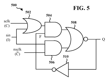
[0023] FIG. 5 is a diagram illustrating an exemplary configuration for
the scan latch
500. As shown in FIG. 5, the scan latch 500 includes an OR gate 502, an AND
gate
504, an AND gate 506, a NOR gate 508, and an inverter 510. The OR gate 502 has
a first input coupled to a scan clock sclk (C) and a second input coupled to a
scan
input sin (I). An output of the OR gate 502 is coupled to a first input of the
AND
gate 504. The AND gate 506 has a first input coupled to the scan input sin (I)
and a
second input coupled to an inverse scan clock sclk (C). An output of the AND
gate
504 is coupled to a first input of the NOR gate 508, and an output of the AND
gate
506 is coupled to a second input of the NOR gate 508. An output of the NOR
gate
508 is labeled Q. The output Q of the NOR gate 508 is input to the inverter
510. An
output of the inverter 510, labeled as a latch feedback F, is coupled to a
second
input of the AND gate 504. Alternatively, the inverter 510 may be replaced by
a
NAND gate with a shift input set to high during operation of the scan latch
500 (see
the NAND gate 624 of FIG. 6, infra). The latch feedback F is functionally Q,
where
Q is functionally (C + /)F + IC. The symbol "+" is an OR operation, and is the
same as V; the AND operation is the same as A. As such, Q is functionally
((CV/)AF)V(/AC).
[0024] Other configurations are possible consistent with F being
functionally Q and Q
being functionally (C + /)F +IC. For example, the OR gate 502 and the AND gate
504 may be replaced by a first AND gate with inputs C and F, a second AND gate
with inputs I and F, and an OR gate with inputs from the outputs of the first
AND
gate and the second AND gate. As such, logically, (C + /)F is the same as CF +
IF. Further, generally, AB is logically the same as A+ B, and A+B is the same
as
AB. As such, the AND gate 506 with logical operation IC may be replaced with
an
inverter with input I, and a NOR gate receiving as inputs the output of the
inverter
(I) and the scan clock sclk (C).
[0025] The truth table for the scan latch 500 is shown in FIG. 5. When
the scan clock
sclk C is low, the output Q is high when the scan input sin I is low, and the
output Q
is low when the scan input sin I is high. When the scan clock sclk C is high,
the
value at Q is stored (no change of state). The scan latch 500 may be
considered a
set-reset (SR) latch, where set occurs when the scan clock sclk C is low and
the scan
6
CA 02986231 2017-11-15
WO 2016/200468
PCT/US2016/025163
input sin I is low, and reset occurs when the scan clock sclk C is low and the
scan
input sin us high.
[0026] The scan latch 500 is slower than a typical latch / flip-flop,
and avoids issues in
relation to an insufficient hold-margin within a corresponding functional
latch.
Specifically, when the scan latch 102 is the scan latch 500, the functional
latch 106
is less likely to encounter hold-margin issues during a scan mode. Further,
when the
scan latch 202 is the scan latch 500, the functional latch 206 is less likely
to
encounter hold-margin issues during a scan mode. The scan latch 500 also has a
more compact layout than typical scan latches, as discussed infra in relation
to FIG.
7.
[0027] FIG. 6 is a circuit diagram illustrating a second exemplary
circuit configuration
for the master/slave latch configuration of FIG. 2. The scan latch 500 is
indicated as
602. The scan latch 602 includes p-type metal oxide semiconductor (MOS) (pMOS)
transistors 604, 606, 608, 610, and 612, and n-type MOS (nMOS) transistors
614,
616, 618, 620, and 622. The pMOS transistor 604 has a source connected to Vdd,
a
gate connected to a scan clock sclk (C), and a drain coupled to the source of
the
pMOS transistor 608. The pMOS transistor 608 has a gate connected to a scan
input
sin (I), and a drain connected to node A. The pMOS transistor 610 is connected
in
parallel with the pMOS transistor 612, as the source of the pMOS transistor
610 and
the source of the pMOS transistor 612 are connected together and to node A,
and the
drain of the pMOS transistor 610 and the drain of the pMOS transistor 612 are
connected together and to node B. The gate of the pMOS transistor 610 is
connected to the scan input sin (I). The gate of the pMOS transistor 612 is
connected to an inverse scan clock nsclk (C). The pMOS transistor 606 has a
source
connected to Vdd, a drain connected to the node A, and a gate connected to
node F.
The nMOS transistor 614 has a drain connected to node B, a gate connected to
the
inverse scan clock nsclk (C), and a source connected to the drain of the nMOS
transistor 618. The nMOS transistor 618 has a gate connected to the scan input
sin
(I), and a source connected to Vss. The nMOS transistor 620 and the nMOS
transistor 622 are connected in parallel, with the source of the nMOS
transistor 620
connected to the source of the nMOS transistor 622 and to Vss, and with the
drain of
the nMOS transistor 620 connected to the drain of the nMOS transistor 622 and
to
node E. The gate of the nMOS transistor 620 is connected to the scan input sin
(I).
7
CA 02986231 2017-11-15
WO 2016/200468
PCT/US2016/025163
The gate of the nMOS transistor 622 is connected to the scan clock sclk (C).
The
nMOS transistor 616 has a drain connected to node B, a source connected to
node E,
and a gate connected to node F. Node F is a feedback path output from the NAND
gate 624. When the shift input is high, the NAND gate 624 operates as an
inverter.
The NAND gate 624 may be replaced by an inverter, as shown in FIG. 5 by the
inverter 510. During a functional mode, the shift may be set low. Use of the
NAND
gate 624 rather than an inverter 510 saves power during the functional mode.
Specifically, the NAND gate 624 provides approximately a 4% dynamic power
savings (assuming a 15% data activity rate) over use of an inverter 510 during
a
functional mode.
[0028] With respect to remaining portions of the circuit, the nMOS
transistor 626 and
the pMOS transistor 628 operate as a transmission gate based on the scan clock
sclk
(C). The transmission gate 626/628 may be turned on when the scan clock sclk
(C)
is high, and turned off when the scan clock sclk (C) is low. The pMOS
transistor
630 and the nMOS transistor 632 operate as an inverter, and are components of
the
inverter 210 of FIG. 2. The nMOS transistor 634 and the pMOS transistor 636
operate as a transmission gate, and are components of the transmission gate
212 of
FIG. 2. The transmission gate 634/636 may be turned on when the pulse clock
pclk is high, and turned off when the pulse clock pclk is low. The pulse clock
pclk
may be held low during a scan mode, and therefore the transmission gate
634/636
may be off during the scan mode. The pMOS transistor 654 and the nMOS
transistor
656 operate as an inverter, and are components of the inverter 214 of FIG. 2.
The
pMOS transistors 638, 640, and 644, the nMOS transistors 646, 648, and 650,
and
the NOR gate 652 function as the multiplexer 204 and the tri-state inverter
208 of
FIG. 2 and are components of the functional latch 206 of FIG. 2. The reset
input
into the NOR gate 652 is held low during normal operation. When the reset is
set to
high, the output of the NOR gate 652 is low, and upon both the scan clock sclk
(C)
and the pulse clock pclk going low, the node G in the functional latch is set
to high,
and the output 0 is set to low.
[0029] FIG. 7 is a layout diagram illustrating an exemplary layout for
the circuit
configuration of FIG. 6. The scan latch is indicated by 702. The scan latch
702
corresponds to the scan latch 202/602. The scan latch 702 includes 14 scan
devices
(transistors) and extends 9 grids. The scan latch 702 with the transmission
gate
626/628 includes 16 scan devices. The entire layout corresponding to the
circuit
8
CA 02986231 2017-11-15
WO 2016/200468
PCT/US2016/025163
diagram 600 has a width of 24 grids. As discussed supra, a layout with x grids
includes x gate interconnects (e.g., 704 and other equally spaced gate
interconnects)
extending across the cell with the same pitch. If the NAND gate 624 is
replaced
with an inverter (see 510 of FIG. 5), the scan latch 702 would include 12 scan
devices and would extend 8 grids, and the entire layout would extend 23 grids.
As
such, while the scan latch 602 includes more transistors than the scan latch
402, the
scan latch 602 has a more compact layout than the scan latch 402. The less
compact
layout for the scan latch 402 is due to alternating gate connections
associated with
the transmission gate 306 and the keeper stage 308 in the scan latch 402. The
entire
layout for the pulse latch including a parasitic scan latch 602 and the NAND
gate
624 has approximately a 15% area savings (24 grids/28 grids) over the entire
layout
for the pulse latch including a parasitic scan latch 402, and provides
approximately a
10% leakage current savings due to the 15% area reduction. The entire layout
for
the pulse latch including a parasitic scan latch 602 and an inverter 510
instead of the
NAND gate 624 provides approximately an 18% (23 grids/28 grids) area savings
over the entire layout for the pulse latch including a parasitic scan latch
402, but
does not provide the approximately 4% dynamic power savings during a
functional
mode that the scan latch 602 with the NAND gate 624 provides. Accordingly, as
discussed supra, the scan latch 602/500 avoids issues in relation to an
insufficient
hold-margin within a corresponding functional latch by being slower than a
typical/traditional latch / flip-flop. Further, the scan latch 602/500 has a
reduced
area footprint than the scan latch 402/302, and provides leakage current
savings due
to the area reduction.
[0030] Referring again to FIG. 5 and FIG. 6, a MOS device includes a
first latch
configured with one latch feedback F and configured to receive a latch input I
and a
latch clock C. The first latch is configured to output Q, where the output Q
is a
function of CF, IF, and IC, and the latch feedback F is a function of the
output Q.
For example, as shown in FIG. 5, the latch feedback F is functionally Q, and
the
output Q is functionally (C + /)F + I C . As discussed supra, (C + 1)F is the
same
as CF + IF. As such, the scan latch 500 is a function of CF, IF, and IC.
[0031] In one configuration, the first latch includes a first set of
transistors stacked in
series, and the first set of transistors includes at least five transistors.
For example,
as shown in FIG. 6, the first set of transistors includes the pMOS transistors
604,
9
CA 02986231 2017-11-15
WO 2016/200468
PCT/US2016/025163
608, and 610, and includes the nMOS transistors 614 and 618. The pMOS/nMOS
transistors 604, 608, 610, 614, and 618 are stacked in series. In one
configuration,
the first set of transistors includes at least three pMOS transistors (604,
608, 610)
and at least two nMOS transistors (614, 618). The stacking of these
transistors may
provide some layout benefits for reducing the area/footprint of the layout. In
one
configuration, each transistor of the first set of transistors is coupled to
one of the
latch input I, the latch clock C, or an inverse latch clock C. For example,
the pMOS
transistor 604 is coupled to the scan clock sclk C, the pMOS transistor 608 is
coupled to the scan input I, the pMOS transistor 610 is coupled to the scan
input I,
the nMOS transistor 614 is coupled to the inverse scan clock nsclk C, and the
nMOS
transistor 618 is coupled to the scan input I. In one configuration, the first
latch
further includes a second set of transistors stacked in series. The second set
of
transistors includes at least three transistors. For example, the pMOS
transistor 606,
the pMOS transistor 612, and the nMOS transistor 616 are stacked in series.
The
second set of transistors includes at least two pMOS transistors (606, 612)
and at
least one nMOS transistor (616). The stacking of these transistors may provide
some layout benefits for reducing the area/footprint of the layout. In one
configuration, each transistor of the second set of transistors is coupled to
one of the
latch feedback F, or an inverse latch clock C. For example, the pMOS
transistor
606 is coupled to the latch feedback F, the pMOS transistor 612 is coupled to
the
inverse scan clock nsclk C, and the nMOS transistor 616 is coupled to the
latch
feedback F. In one configuration, the first latch further comprises a third
set of
transistors in parallel. The third set of transistors is stacked in series
with the second
set of transistors. For example, the third set of transistors includes the
nMOS
transistors 620 and 622 connected in parallel. The nMOS transistors 620 and
622
are stacked in series with the second set of transistors 606, 612, 616. The
stacking
of the second and third sets of transistors may provide some layout benefits
for
reducing the area/footprint of the layout. In one configuration, each
transistor of the
third set of transistors is coupled to one of the latch input I, or the latch
clock C. For
example, the nMOS transistor 620 is coupled to the scan input sin I, and the
nMOS
transistor 622 is coupled to the scan clock sclk C.
[0032] In one configuration, the first latch includes a first pMOS
transistor 610 having a
first pMOS transistor source, a first pMOS transistor gate, and a first pMOS
CA 02986231 2017-11-15
WO 2016/200468
PCT/US2016/025163
transistor drain. The first pMOS transistor gate is coupled to the latch input
I. The
first latch includes a second pMOS transistor 612 having a second pMOS
transistor
source, a second pMOS transistor gate, and a second pMOS transistor drain. The
second pMOS transistor gate is coupled to an inverse latch clock C. The second
pMOS transistor source is coupled to the first pMOS transistor source at node
A.
The second pMOS transistor drain is coupled to the first pMOS transistor drain
at
node B. The first latch includes a first nMOS transistor 614 having a first
nMOS
transistor source, a first nMOS transistor gate, and a first nMOS transistor
drain.
The first nMOS transistor drain is coupled to the first pMOS transistor drain
and the
second pMOS transistor drain at node B. The first latch includes a second nMOS
transistor 618 having a second nMOS transistor source, a second nMOS
transistor
gate, and a second nMOS transistor drain. The second nMOS transistor drain is
coupled to the first nMOS transistor source. The second nMOS transistor source
is
coupled to a first voltage source Vss. The first nMOS transistor gate is
coupled to
one of the latch input / or the inverse latch clock C, and the second nMOS
transistor
gate is coupled to an other one of the latch input / or the inverse latch
clock C. As
shown in FIG. 6, the first nMOS transistor gate is coupled to the inverse
latch clock
C, and the second nMOS transistor gate is coupled to the latch input I.
However,
alternatively, the first nMOS transistor gate may be coupled to the latch
input /, and
the second nMOS transistor gate may be coupled to the inverse latch clock C.
[0033] In one configuration, the first latch further includes a third
pMOS transistor 604
having a third pMOS transistor source, a third pMOS transistor gate, and a
third
pMOS transistor drain. The third pMOS transistor source is coupled to a second
voltage source Vdd. The first latch further includes a fourth pMOS transistor
608
having a fourth pMOS transistor source, a fourth pMOS transistor gate, and a
fourth
pMOS transistor drain. The fourth pMOS transistor source is coupled to the
third
pMOS transistor drain. The fourth pMOS transistor drain is coupled to the
first
pMOS transistor source and the second pMOS transistor source at node A. The
third pMOS transistor gate is coupled to one of the latch input / or the latch
clock C,
and the fourth pMOS transistor gate is coupled to an other one of the latch
input / or
the latch clock C. As shown in FIG. 6, the third pMOS transistor gate is
coupled to
the latch clock C, and the fourth pMOS transistor gate is coupled to the latch
input I.
11
CA 02986231 2017-11-15
WO 2016/200468
PCT/US2016/025163
However, alternatively, the third pMOS transistor gate may be coupled to the
latch
input I, and the fourth pMOS transistor gate may be coupled to the latch clock
C.
[0034] In one configuration, the first latch further includes a third
nMOS transistor 620
having a third nMOS transistor source, a third nMOS transistor gate, and a
third
nMOS transistor drain. The third nMOS transistor source is coupled to the
first
voltage source Vss. The third nMOS transistor gate is coupled to the latch
input I.
The first latch further includes a fourth nMOS transistor 622 having a fourth
nMOS
transistor source, a fourth nMOS transistor gate, and a fourth nMOS transistor
drain.
The fourth nMOS transistor source is coupled to the first voltage source Vss.
The
fourth nMOS transistor drain is coupled to the third nMOS transistor drain at
node
E. The fourth nMOS transistor gate is coupled to the latch clock C.
[0035] In one configuration, the first latch further includes a fifth
pMOS transistor 606
having a fifth pMOS transistor source, a fifth pMOS transistor gate, and a
fifth
pMOS transistor drain. The fifth pMOS transistor source is coupled to the
second
voltage source Vdd. The fifth pMOS transistor drain is coupled to the first
pMOS
transistor source and the second pMOS transistor source at node A. The fifth
pMOS
transistor gate is coupled to the latch feedback F. The first latch further
includes a
fifth nMOS transistor 616 having a fifth nMOS transistor source, a fifth nMOS
transistor gate, and a fifth nMOS transistor drain. The fifth nMOS transistor
source
is coupled to the third nMOS transistor drain and the fourth nMOS transistor
drain at
node E. The fifth nMOS transistor drain is coupled to the first pMOS
transistor
drain and the second pMOS transistor drain at node B. The fifth nMOS
transistor
gate is coupled to the latch feedback F.
[0036] In one configuration, the first latch further includes a NAND
gate 624 with a
first NAND gate input, a second NAND gate input, and a NAND gate output. The
first NAND gate input is coupled to the first pMOS transistor drain, the
second
pMOS transistor drain, the first nMOS transistor drain, and the fifth nMOS
transistor drain at node B. The second NAND gate input is coupled to a shift
input.
The NAND gate output is the latch feedback F. Alternatively, in one
configuration,
the first latch further includes an inverter 510 with an inverter input and an
inverter
output. The inverter input is coupled to the first pMOS transistor drain, the
second
pMOS transistor drain, the first nMOS transistor drain, and the fifth nMOS
transistor drain at node B. The inverter output is the latch feedback F.
12
CA 02986231 2017-11-15
WO 2016/200468
PCT/US2016/025163
[0037] In one
configuration, the MOS device further includes a second latch (e.g., 106,
206, and the components in FIG. 6 of the functional latch 206). The second
latch is
configured as a latch in a scan mode and as a pulse latch in a functional
mode. The
second latch is configured to be clocked with a scan clock sclk in the scan
mode and
with a pulse clock pclk in the functional mode. The pulse clock pclk is
different
than the scan clock sclk. In one configuration, the first latch operates as a
master
latch and the second latch operates as a slave latch during the scan mode. In
one
configuration, the first latch has a width of at least eight grids including
at least eight
gate interconnects that extend across the device. For example, the first latch
602
may have a width of nine grids when the latch 602 includes the NAND gate 624,
and may have a width of eight grids when the latch 602 includes an inverter
(e.g.,
510) instead of the NAND gate 624 in the feedback path for F. In one
configuration, each of at least five gate interconnects of the at least eight
gate
interconnects is shared between one pMOS transistor and one nMOS transistor.
For
example, the pMOS transistor 604 and the nMOS transistor 622 may share the
same
gate interconnect, and the pMOS transistor 612 and the nMOS transistor 614 may
share the same gate interconnect. For another example, the pMOS transistor 608
may share a gate interconnect with one of the nMOS transistor 618 or the nMOS
transistor 620, and the pMOS transistor 610 may share a gate interconnect with
an
other one of the nMOS transistor 618 or the nMOS transistor 620.
[0038] FIG. 8 is a flowchart of an exemplary method of an exemplary MOS
device
associated with at least one of FIGs. 1, 2, 5, 6, and 7. At 802, the MOS
device
receives a latch input I and a latch clock C at a first latch. At 804, the MOS
device,
outputs, at the first latch, an output Q and one latch feedback F to the first
latch
based on the output Q. The latch feedback F is a function of the output Q. The
output Q is a function of CF, IF, and IC. The latch feedback F may be
functionally
Q. The
output Q may be functionally (C + /)F + IC. As discussed supra in
relation to FIG. 6, the first latch may include a first set of transistors
604, 608, 610,
614, 618 stacked in series, where the first set of transistors includes at
least five
transistors. Referring to FIGs. 1, 2, the output Q may be outputted to a
second latch
106/206 coupled to the first latch 102/202. The second latch 106/206 is
configured
as a latch in a scan mode and as a pulse latch in a functional mode.
13
CA 02986231 2017-11-15
WO 2016/200468
PCT/US2016/025163
[0039] In one
configuration, a MOS device includes means for receiving a latch input I
and a latch clock C at a first latch. In addition, the MOS device includes
means for
outputting, at the first latch, an output Q and one latch feedback F to the
first latch
based on the output Q. The latch feedback F is a function of the output Q. The
output Q is a function of CF, IF, and IC. For example, referring to FIG. 5,
the OR
gate 502 receives a latch input I and a latch clock C. In addition, the NOR
gate 508
outputs the output Q and the inverter 510 outputs one latch feedback F to the
first
latch 500 based on the output Q. In the first latch 500, the latch feedback F
is a
function of the output Q, and the output Q is a function of CF, IF, and IC.
Specifically, as discussed supra, the latch feedback F is functionally Q, and
the
output Q is functionally (C + /)F + IC. As
discussed supra, different
configurations of the latch 500 are possible consistent with the feedback F
being
functionally Q, and the output Q being functionally (C + /)F + IC.
[0040] It is
understood that the specific order or hierarchy of steps in the processes
disclosed is an illustration of exemplary approaches. Based
upon design
preferences, it is understood that the specific order or hierarchy of steps in
the
processes may be rearranged. Further, some steps may be combined or omitted.
The accompanying method claims present elements of the various steps in a
sample
order, and are not meant to be limited to the specific order or hierarchy
presented.
[0041] The previous description is provided to enable any person
skilled in the art to
practice the various aspects described herein. Various modifications to these
aspects
will be readily apparent to those skilled in the art, and the generic
principles defined
herein may be applied to other aspects. Thus, the claims are not intended to
be
limited to the aspects shown herein, but is to be accorded the full scope
consistent
with the language claims, wherein reference to an element in the singular is
not
intended to mean "one and only one" unless specifically so stated, but rather
"one or
more." The word "exemplary" is used herein to mean "serving as an example,
instance, or illustration." Any aspect described herein as "exemplary" is not
necessarily to be construed as preferred or advantageous over other aspects."
Unless
specifically stated otherwise, the term "some" refers to one or more.
Combinations
such as "at least one of A, B, or C," "at least one of A, B, and C," and "A,
B, C, or
any combination thereof' include any combination of A, B, and/or C, and may
include multiples of A, multiples of B, or multiples of C. Specifically,
combinations
14
CA 02986231 2017-11-15
WO 2016/200468
PCT/US2016/025163
such as "at least one of A, B, or C," "at least one of A, B, and C," and "A,
B, C, or
any combination thereof' may be A only, B only, C only, A and B, A and C, B
and
C, or A and B and C, where any such combinations may contain one or more
member or members of A, B, or C. The term "connected" means "directly
connected." The term "coupled" means "connected" or "indirectly connected"
through other elements. All structural and functional equivalents to the
elements of
the various aspects described throughout this disclosure that are known or
later
come to be known to those of ordinary skill in the art are expressly
incorporated
herein by reference and are intended to be encompassed by the claims.
Moreover,
nothing disclosed herein is intended to be dedicated to the public regardless
of
whether such disclosure is explicitly recited in the claims. No claim element
is to be
construed as a means plus function unless the element is expressly recited
using the
phrase "means for."