Note: Descriptions are shown in the official language in which they were submitted.
CA 02986387 2017-11-17
WO 2016/187090
PCT/US2016/032630
VOLTAGE SENSOR
TECHNICAL FIELD
The invention relates to a voltage sensor for powerline and/or cable
accessories
applications.
BACKGROUND
As electrical power distribution becomes more complex through the advent of
renewable
energy, distributed generation and the adoption of electric vehicles,
intelligent electrical
distribution and associated electrical sensing is becoming more useful and
even necessary.
Useful sensing may include, for example, voltage, current, and the time
relationship between
voltage and current at various locations within a power distribution network.
SUMMARY
In general, this disclosure is directed to a voltage sensor that can be
connected to a power
line, cable, or cable accessories. In particular, a voltage sensor, comprises
a conductor having a
first end and a second end, the first end including a first connection
interface and the second end
having no connection, and a sensor section including at least one sensor
disposed over the
conductor between the first and second ends, the sensor sensing at least a
voltage or a sample of
the voltage of the conductor.
In one aspect, the second end has reduced electric field stress concentration.
In a further
aspect, the second end of the conductor has a rounded surface, such as a fully
rounded (or semi-
hemispherical) surface. In a further aspect, the second end includes a bulbous
rounded surface.
In one aspect, the sensor section includes a voltage sensor. A first electrode
of the
voltage sensor can comprise the conductor. Alternatively, the first electrode
of the voltage
sensor comprises an inner shield layer in contact with the conductor. The
voltage sensor further
includes an insulation layer disposed over the isolated inner shield layer,
and an electrically
isolated outer shield layer disposed over the insulation layer.
The above summary of the present invention is not intended to describe each
illustrated
embodiment or every implementation of the present invention. The details of
one or more
examples of this disclosure are set forth in the accompanying drawings and the
description
below. Other features, objects, and advantages of the disclosed techniques
will be apparent from
the description and drawings, and from the claims.
-1-
CA 02986387 2017-11-17
WO 2016/187090
PCT/US2016/032630
BRIEF DESCRIPTION OF DRAWINGS
Fig. 1 is a cut away view of a voltage sensor according to an aspect of the
present
invention.
Fig. 2 is a close-up section view of the sensing section of the voltage sensor
according to
another aspect of the present invention.
Fig. 3 is a close-up, cross section view of the voltage sensor according to
another aspect
of the present invention.
DETAILED DESCRIPTION
In the following Detailed Description, reference is made to the accompanying
drawings,
which form a part hereof, and in which is shown by way of illustration
specific embodiments in
which the invention may be practiced. In this regard, directional terminology,
such as "top,"
"bottom," "front," "back," "leading," "forward," "trailing," etc., is used
with reference to the
orientation of the Figure(s) being described. Because components of
embodiments of the present
invention can be positioned in a number of different orientations, the
directional terminology is
used for purposes of illustration and is in no way limiting. It is to be
understood that other
embodiments may be utilized and structural or logical changes may be made
without departing
from the scope of the present invention. The following detailed description,
therefore, is not to
be taken in a limiting sense, and the scope of the present invention is
defined by the appended
claims.
The present disclosure describes a voltage sensor that can be used, for
example, to
measure the voltage of a power line, such as an overhead power line, at a
particular location,
such as a capacitor bank, switch or protective device, such as an overhead
switch (manual or
actuated by a motor, solenoid, etc.), a sectionalizer or recloser, or a
voltage regulation
transformer, etc. In one aspect, the voltage sensor utilizes an integrated,
high accuracy
capacitive voltage sensor. The voltage sensor can have a compact design and
can be coupled to
an existing power line (conductor or cable) in a straightforward manner. The
voltage sensor
described herein can provide a compact mechanism for providing real time, high
accuracy
voltage characteristics of a power cable or location in an electrical grid.
The output of the
voltage sensor can be a waveform that is directly proportional to the voltage
of the power line.
The division ratio of the actual line voltage to the output voltage can be
tailored to any desired
voltage. In some embodiments, the division ratio can be between 1:1 and
1,000,000:1; in other
preferred embodiments, the division ratio can be approximately 10,000:1, where
for example an
actual line voltage of approximately 10,000 Volts would result in an output
voltage of
-2-
CA 02986387 2017-11-17
WO 2016/187090
PCT/US2016/032630
approximately 1 Volt. The voltage sensor supplies a voltage level that can in
some embodiments
be easily converted to a digital value for interaction with computational
devices,
microcontrollers, communication devices, etc. The voltage sensor can thus
provide a utility,
solar farm, wind farm, ship, industrial plant, or any individual or company
that uses medium or
high voltage equipment with an easy access to obtain a real time voltage
reading of a live power
line, as well as the ability to create a smart node at many different grid
locations.
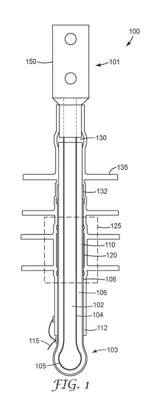
FIG. 1 shows a first aspect of the invention, voltage sensor 100.
Voltage sensor 100 includes a conductor (also referred to as an inner
conductor) 102,
which may be a solid or stranded metal axial conductor such as an aluminum or
copper alloy
conductor. Inner conductor 102 includes a first end 101, which can include a
first connection
interface 150 and a second end 103. The second end 103 has no connection. In
one aspect, the
second end is shaped to allow for optimal stress control in a minimal space
with ease, to
substantially reduce the probability of partial discharge or electrical
failure. In one aspect,
second end 103 includes a rounded surface 105, such as a fully rounded surface
(i.e., having no
or almost no sharp edges). This rounded surface shape reduces electric field
stress
concentration. In one example configuration, such as shown in Fig. 1, the
rounded surface 105
has a bulbous shape. Alternatively, depending on the size of conductor 102, if
conductor 102 is
of large enough diameter, a bulbous end can be omitted. Instead, in some
embodiments, a full
radius (semi-hemisphere) can be formed from the end 103 of the conductor. This
semi-
hemispherical shape would also remove any sharp edges that can lead to
electric stress
concentrations. In a further alternative aspect, the second end 103 of the
voltage sensor 100 can
be covered with a molded semiconducting rubber or semiconducting plastic
material. In this
alternative aspect, the semiconducting molding can be used to cover a rounded
surface or a sharp
surface.
The first connection interface 150 can include a lug, which is shown in Fig.
1.
Alternatively, the connection interface can comprise a separable connector, a
splice, a modular
connector, or other connection interfaces.
The connection interface can have a circular cross section configured to mate
to a male
end of conductor 102. In alternative aspects, the first end of the conductor
102 can be formed as
a male or hybrid type connector.
As shown in Fig. 1, connection interface 150 comprises a lug. The structure of
Fig. 1
allows for straightforward mechanical fastening and electrical conduction (or
path) from an
overhead power cable or line. For example, one method of attaching the voltage
sensor 100 to
an overhead line is to use a conventional overhead primary tap (such as a
BHF/AHF two hole
-3-
CA 02986387 2017-11-17
WO 2016/187090
PCT/US2016/032630
hot line pad connector available from Hubbell Power Systems, USA) and bolt
that connector to
connection interface/lug 150. Alternatively, a conventional stem connector can
be used. As
such, voltage sensor 100 can be installed at any point along a power cable,
line or in a cable
accessory.
Moreover, voltage sensor 100 is configured to control the electrical field
created by
medium or high voltage within a power line or cable, such as an overhead power
line or cable,
wherein the power line or cable operates at voltages in excess of 1,000 Volts.
As shown in Fig.
1, a high K layer 132 can be employed to control the electric field.
Alternatively, voltage sensor
100 can include geometric stress control (not shown).
Optionally, in some aspects, inner conductor 102 may be radially surrounded by
conductor shield layer 104. Conductor shield layer 104 comprises a conductive
or semi-
conductive material that is configured to smooth out any conductor surface
inconsistencies that
could create high electric field stress concentrations, especially when
sensing the voltage of a
medium or high voltage line or cable, which could cause a reduction in
accuracy or possible
sensor failure. In one aspect, the outer surface of the conductor shield layer
104 is smooth. As
will be described in further detail below, the inner conductor 102 and
optional inner shield layer
104 provide one electrode of a capacitor for the sensor section. The other
electrode of the
capacitor is formed by the isolated section 110 of insulation shield layer
108, and insulation
layer(s) 106 serves as the dielectric of the capacitor.
Voltage sensor 100 further includes insulation layer 106, which concentrically
surrounds
conductor shield layer 104. The insulation layer 106 can be formed from a
conventional
dielectric material, such as elastomeric silicone, ethylene propylene diene
monomer rubber
(EPDM), hybrids or combinations thereof Alternatively, insulation layer 106
can comprise
more than 1 layer of insulation material, such as first and second insulation
layers (not shown),
with each layer being formed from a different or same insulation material. The
optional semi-
conductive or conductive shield layer 104 functions to eliminate or reduce the
potential for voids
between conductor 102 and insulation layer(s) 106 that might allow leakage
leading to
degradation of insulation layer(s) 106. Shield layer 104 may also relieve
electrical stresses
caused by any roughness on the surface of the inner conductor 102 due to, for
example,
manufacturing processes such as casting.
In an alternative aspect, conductive layer 102 can have a highly smooth outer
surface. As
such, an adhesive or other bonding material can be interposed between the
conductive layer 102
and the insulation layer 106, with the shield layer 104 being omitted. The
adhesive or other
-4-
CA 02986387 2017-11-17
WO 2016/187090
PCT/US2016/032630
bonding material can be applied to the outer surface of conductor 102 and can
bond the
insulation layer 106 to the conductive layer 102.
In addition, an insulation shield layer 108 is provided and concentrically
surrounds
insulation layer 106. The insulation shield layer 108 comprises a conductive
or semiconductive
material formed as a layer adjacent to and concentrically surrounding
insulation layer 106. As
described below, for purposes of the sensing section 125, this insulation
layer 106 also forms the
insulation layer of a capacitor, which also comprises the inner conductor 102
and/or conductor
shield layer 104 and isolated section 110 of insulation shield layer 108.
Isolated section of
insulation shield layer 110 is isolated from the ground potential of the
remainder of insulation
shield layer 108.
In the embodiment of Fig. 1, voltage sensor 100 further comprises a tubular
sleeve 112
that extends over at least a portion of the conductor/inner
shield/insulation/shield structure and
the sensor section 125. In one aspect, tubular sleeve 112 comprises a suitable
cold-shrinkable
material, such as a highly elastic rubber material that has a low permanent
set, such as EPDM,
elastomeric silicone, electrical grade resin, or a hybrid thereof Insulation
layer 106 and tubular
sleeve can be made of the same or different types of materials. The semi-
conductive and
insulating materials may have differing degrees of conductivity and insulation
based on the
inherent properties of the materials used or based on additives added to the
materials. Tubular
sleeve 112 may also be made from a suitable heat-shrinkable material.
Alternatively, the tubular
sleeve 112 may be an overmolded or push-on layer. A ground reference wire 115
can also be
provided. Optionally, in the illustrated embodiment, tubular sleeve 112
includes skirts 135
which serve to reduce leakage current and which is particularly useful for
outdoor applications.
In some embodiments, tubular sleeve 112 can also cover rounded end 103.
In addition, a sealing compound 130 can be provided to create an environmental
seal and
prevent moisture from migrating into the area between the insulation layer 106
and the
connection interface/lug 150.
As shown in Fig. 1, and in greater detail in Fig. 2, voltage sensor 100
includes a sensor
section 125 disposed between the first and second ends of conductor 102. In
one aspect, the
sensing section includes a voltage sensor, such as an impedance voltage
divider that utilizes
complex impedance based voltage division, or a capacitive voltage sensing
device, having an
electrically isolated capacitive voltage sensor. More generally, in at least
one aspect, where the
sensing section includes an impedance voltage divider, a first impedance and a
second
impedance are connected in series. The input voltage is applied across the
series impedances and
the output voltage is the voltage across the second impedance. The first and
second impedances
-5-
CA 02986387 2017-11-17
WO 2016/187090
PCT/US2016/032630
may be composed of any combination of elements such as resistors, inductors
and capacitors. In
at least one aspect, the sensing section includes a multi-component AC
circuit, wherein the
response can be complex and can have imaginary components. In another aspect,
the sensor
section includes at least one temperature compensation component, such as,
e.g., a thermistor.
The temperature sensor (e.g., thermistor) can be located within (or outside
of) the sensing section
125. While one specific embodiment is described below, the sensing section can
also be
configured in a manner similar to the voltage sensors described in
International Publ. Nos.
WO 2015/179285 and WO 2013/096354, each incorporated by reference herein in
their entirety.
Moreover, in a further alternative aspect, the voltage sensor 100 can further
include one or more
additional sensors.
As shown in Fig. 2, the sensing section 125 includes an electrically isolated
section 110
of conductive or semiconductive material (insulation shield) layer 108 in
contact with an outer
surface of insulation layer 106. The electrically isolated section 110 of
conductive or
semiconductive material (insulation shield) layer 108 forms an electrode of a
sensing capacitor
of a capacitive voltage divider or sensor. The electrically isolated section
thus can be
capacitively coupled to the conductor 102 and electrically isolated from
ground potential. In
addition, insulation layer 106 is operable to form a dielectric of the sensing
capacitor of the
capacitive voltage divider or sensor.
In some examples, the electrically isolated section 110 may be in an annular
ring
configuration and be electrically isolated from conductive or semiconductive
shielding layer 108
by non-conductive axial sections 111a and 111b. Non-conductive axial sections
111a, 111b may
comprise non-conductive material or a void.
In such examples, conductive or semiconductive shielding layer 108 may be
discontinuous at two longitudinal positions to form electrically isolated
section 110 in the
annular ring configuration. In such examples, electrically isolated section
110 may be formed out
of a common material and manufacturing process, such that electrically
isolated section 110 and
shield layer 108 have a common thickness.
In other examples, electrically isolated section 110 may be formed from a
different
material than shield layer 108 and/or have a different configuration such as a
rectangular or
round shape formed by a flexible material affixed to insulation layer 106.
Electrically isolated
section 110 may, for example, comprise an electrically conductive metal or an
electrically
conductive polymer. As one example, electrically isolated section 110 may
comprise a layer of
copper. In some examples, voltage sensor 100 may include an adhesive that
affixes electrically
isolated section 110 to insulation layer 106. In some examples, electrically
isolated section 110
-6-
CA 02986387 2017-11-17
WO 2016/187090
PCT/US2016/032630
may further include a conforming rubber insulation or high dielectric constant
tape or a self-
fusing insulation or high K material 127, such as a rubber mastic material, to
prevent moisture
from migrating into the sensor section 125. In some aspects, strips of
insulating or high
dielectric constant material cover gaps 111a, 111b to separate isolated
section 110 from any
other conductive or semiconductive material or elements, except from the PCB
120, and to
prevent the presence of air in gaps 111a, 111b, which air could cause a
partial electrical
discharge and a failure of the voltage sensor. The insulating or high
dielectric constant material
may be any suitable material such as a combination of mastic, which will more
easily fill gaps
111a, 111b, and PVC tape placed over the mastic. In some examples, the
electrically isolated
section 110 may include a heat shrinkable or cold shrinkable material.
In some aspects, inner and outer conductive or semiconductive shield layers
104, 108 and
insulating layer 106 of voltage sensor 100 may be made from any materials
suitable for
shrinkable sleeve applications. Most suitable are materials such as a highly
elastic rubber
material that has a low permanent set, such as ethylene propylene diene
monomer (EPDM),
elastomeric silicone, or a hybrid thereof, that may include conventional
additives to make the
layers appropriately conductive, semiconductive or insulating, as needed. The
conductive or
semiconductive shield layers and the insulation layer may be made of the same
or different types
of materials, depending on the types of additives which may be incorporated in
the individual
layers. The inner and outer conductive or semiconductive shield layers and the
insulation layer
may have differing degrees of conductivity and insulation based on the
inherent properties of the
materials used or based on additives added to the materials.
As mentioned above, in some aspects, the sensor section 125 is configured as a
capacitive
voltage sensor, which is operable to sense a voltage on inner conductor 102,
which is also
representative of the voltage on the power line (not shown) by way of the
connection with the
connection interface 150. Electrically isolated section 110 is operable to
form an electrode of the
sensing capacitor of the capacitive voltage sensor and may, for example, have
two opposed
major surfaces, e.g. first and second major surfaces. The first major surface
may be in
mechanical contact with insulation layer 106. The second major surface may be
in mechanical
contact with a capacitive element, such as a capacitor, circuitry, or a
printed circuit board (PCB)
120. In many aspects, the capacitive element, such as PCB 120, has a pre-
defined capacitance
value.
As mentioned previously, the output of the voltage sensor can be a waveform
that is
directly proportional to the voltage of the power line. The division ratio of
the actual line
voltage to the output voltage can be tailored to any desired voltage. In some
embodiments, the
-7-
CA 02986387 2017-11-17
WO 2016/187090
PCT/US2016/032630
division ratio can be between 1:1 and 1,000,000:1; in other aspects, the
division ratio can be
approximately 10,000:1, where for example an actual line voltage of
approximately 10,000 Volts
would result in an output voltage of approximately 1 Volt. The voltage sensor
100 supplies a
voltage level that can in some embodiments be easily converted to a digital
value for interaction
with computational devices, microcontrollers, communication devices, etc.
The capacitive voltage sensor further includes capacitive element (here PCB
120), which
is in electrical contact with electrically isolated section 110. In one
aspect, the PCB 120 is
located close to or directly over the electrically isolated section 110 to
arrange for the electrical
contact with the isolated section 110, which in turn is arranged on insulation
layer 106. PCB 120
further includes at least one additional capacitor or other capacitive element
to form a capacitive
voltage divider for determining the voltage of inner conductor 102 by way of
the detected
voltage of electrically isolated section 110. The capacitor(s) of PCB 120 may
be electrically
connected to electrically isolated section 110. The capacitive element may be
operable as a
secondary capacitor in a capacitive voltage divider. The capacitive voltage
divider may comprise
the sensing capacitor, which includes electrically isolated section 110, and
the secondary
capacitor.
In some aspects, PCB 120 may be flexible such that PCB 120 may be bent to
conform
around electrically isolated section 110. PCB 120 may establish electrical
contact to electrically
isolated section 110 in several locations. This construction avoids the
disadvantages of having
electrical contact only in one location on electrically isolated section 110,
such as, problems
resulting from a bad electrical contact in the one location, if that one
contact is, e.g., incomplete,
corroded, or damaged, which might preclude a voltage reading. In addition
providing multiple
points of contact may avoids problems arising from the fact that electrons
travelling from a rim
of electrically isolated section 110 to a single contact location experience
the electrical resistance
of electrically isolated section 110 over a longer path. This, in turn, may
lead to a voltage drop
and eventually to a lower, i.e. less accurate, voltage being measured on PCB
120.
In some examples, PCB 120 may be mechanically attached to electrically
isolated section
110. In other examples, PCB 120 may alternatively be in a pressure contact
with electrically
isolated section 110. PCB 120 may comprise a double-sided PCB, i.e. PCB 120
can have
opposed first and second major sides. Alternatively the PCB 120 can be located
remotely from
the isolated section 110, where the PCB 120 can be electrically coupled to the
isolated section
110.
For example, as further illustrated in Fig. 3, PCB 120 can comprise a
multilayer structure,
with a first layer 120a comprising a conductive metal, e.g. gold, silver, or
copper; a second layer
-8-
CA 02986387 2017-11-17
WO 2016/187090
PCT/US2016/032630
120b comprising a flexible insulation material; a third layer or conductive
trace 120c to connect
to jumper wires 122; a fourth layer 120d comprising an outer insulation layer;
and an outer
conductive shield layer 120e comprising a conductive or semiconductive layer
which shields
PCB 120.
In one example, the first layer 120a can comprise a copper layer that may be
gold-plated
for enhanced electrical contact and/or for protection against environmental
influences, e.g.
against corrosion. In different examples, first PCB layer 120a comprises a
conductive region
that provides a continuous surface contact area or a patterned, i.e.
interrupted, non-continuous,
surface contact area for contact with electrically isolated section 110. All
parts of the patterned
surface contact area may be electrically connected with each other. A
patterned surface contact
area may require less conductive material for manufacturing it, while having
only a negligible
influence on reliability of the electrical contact and resistive losses.
PCB 120 may comprise a flexible portion. A patterned surface contact area may
also
enhance the mechanical flexibility of PCB 120, thus reducing the risk of layer
cracking and/or
flaking, when PCB 120 is bent. In a specific example, the first PCB layer 120a
comprises a
patterned gold-plated copper layer. A pattern of the surface contact area may,
for example, be a
grid with a square-shaped or a diamond-shaped pattern.
The PCB 120 may further comprise a second layer 120b comprising a flexible
insulating
material, such as a conventional, flexible insulation material.
A flexible portion of PCB 120 and in particular a flexible PCB may allow PCB
120 to
conform better to electrically isolated section 110. This, in turn, enhances
the electrical contact
between PCB 120 and electrically isolated section 110 and thereby makes the
contact more
reliable, reduces resistive losses, and facilitates higher accuracy of the
voltage sensor.
A conductive trace 120c connects with jumper wires 122, which are connected to
ground
on either side of the isolated section 110 by conductive tape/adhesive 109
disposed on shield
layer 108. The conductive tape/adhesive 109 provides adequate surface area.
The outer shield layer 120e can comprise a conductive or semiconductive
material and is
grounded to conductive tape/adhesive 109, as shown in Fig. 3.
Although not shown, PCB 120 may further include a plurality of ratio
adjustment
capacitors.
PCB 120 may generate a signal that is indicative of the voltage of inner
conductor 102.
Sensor signal wire 124 can be connected to PCB 120 for transmitting the sensor
voltage signal
from PCB 120. In some examples, electrical measurement circuitry may be
incorporated into the
PCB 120; in other examples, PCB 120 may include electrical measurement
circuitry. Sensor
-9-
CA 02986387 2017-11-17
WO 2016/187090
PCT/US2016/032630
signal wire 124 they may be connected to, for example, a remote terminal unit
that processes
voltage data from the sensor section 125, or an integrator, a measuring
device, a control device,
or other suitable types of devices.
A ground reference wire 122 may be used to bring ground onto PCB 120 for
connecting
electrical ground to the electrical measurement circuitry. In one aspect,
ground reference wire
122 is connected to a conductive trace of PCB 120, such as conductive trace
120c shown in Fig.
3. This configuration brings a bridging connection between the insulation
shield layers on either
side of isolated section 110. The electric measurement circuitry may be
operational to determine
the voltage of inner conductor 102 versus ground.
In some examples, PCB 120 may be adapted to support additional sensing such as
temperature, humidity, magnetic field, etc.
In an alternative aspect, PCB 120 can be directly disposed on insulation layer
106, such
that the isolated section 110 of the shielding layer 108 can be eliminated. In
a further alternative
aspect, PCB 120 can be disposed directly on insulation layer 106 at a position
beyond an end of
the shielding layer 108.
In one aspect, the sensor section 125 further includes a sensor insulation
layer 126 that is
disposed adjacent to the isolated section 110. In another aspect, the sensor
insulation layer 126
can be adjacent to the PCB 120 and on the opposing side of PCB 120 relative to
electrically
isolated section 110. The sensor insulation layer 126 helps to prevent the PCB
120 from
shorting out.
In a further aspect, the sensor section 125 further includes a sensor (outer)
shielding layer
128 that is disposed adjacent to sensor insulation layer 126 on the opposing
side of sensor
insulation layer 126 relative to PCB 120. Outer sensor shield layer 128 may be
formed from a
conductive or semiconductive material and may be electrically connected to
shield layer 108,
e.g., at ground potential. Outer sensor shield layer 128 provides electric
field shielding to
contain the electric field from the isolated section 110/outer electrode and
from external electric
fields. Outer sensor shield layer 128 and insulation shield layer 108 may
function to
substantially encapsulate the capacitive voltage sensor, including the
electrically isolated section
110, PCB 120 and sensor insulation layer 126. In some examples, outer sensor
shield layer 128
and insulation shield layer 108 may be formed as a unitary feature. In
addition, as shown in Fig.
2, tubular sleeve 112 extends over at least a portion of the sensor section
125.
The precise dimensional control facilitated by the design and configuration of
voltage
sensor 100 allows for precise voltage measurements by the capacitive voltage
sensor of the
sensor section 125. For example, capacitance is directly related to the
geometry of two
-10-
CA 02986387 2017-11-17
WO 2016/187090
PCT/US2016/032630
conductive electrodes and the insulation forming the capacitor. With respect
to the capacitive
voltage sensor, the sensing capacitor is formed from inner conductor 102/inner
shield layer 104,
insulation layer 106 and electrically isolated section 110.
In some examples, voltage sensor 100 may be formed using overmolded
construction.
For example inner shield layer 104 may be overmolded on inner conductor 102.
Similarly,
insulation layer 106 may be an overmolded insulation layer overmolded on inner
shield layer
104 or overmolded directly on inner conductor 102 if inner shield layer 104 is
not included in the
voltage sensor device 100. Likewise, shield layer 108 may be an overmolded
outer conductive or
semiconductive layer overmolded on insulation layer 106. As such, in some
aspects, the
construction can comprise a multilayer body that can be formed as a contiguous
overmolded
body that comprises the insulation layer 106, shield layer 108, the isolated
section 110, and
optionally the inner shield layer 104.
In another aspect, the voltage ratio of the sensing section 125 can be
adjusted by varying
the length of the isolated section 110 or, in an alternative aspect, by
varying the length of the
PCB 120 that replaces isolated section 110. RTV, grease, mastic, or other
insulating or high
dielectric constant materials can be applied to eliminate air gaps/voids
between the PCB 120 and
the cable insulation 106 and/or to eliminate corona discharges.
The voltage sensor described herein can be utilized in a variety of
applications. For
overhead applications, the voltage sensor can be deployed on any section of
the power grid
having a voltage, such as with standard medium or high voltage cable, bus
bars, capacitor banks,
connectors, lugs, jumpers, any component used in a power grid, switches, and
switch gear. In
other applications, the voltage sensor can be used in underground equipment
applications such as
pad mounted transclosures, pad mounted primary metering cabinets, and many
live front pad
mounted or vault-type live front applications. The voltage sensor can also be
used in switch gear
applications, where the gear is considered deadfront underground equipment.
Although specific embodiments have been illustrated and described herein for
purposes
of description of the preferred embodiment, it will be appreciated by those of
ordinary skill in
the art that a wide variety of alternate or equivalent implementations may be
substituted for the
specific embodiments shown and described without departing from the scope of
the present
invention. Those with skill in the art will readily appreciate that the
present invention may be
implemented in a very wide variety of embodiments. This application is
intended to cover any
adaptations or variations of the embodiments discussed herein.
-11-