Note: Descriptions are shown in the official language in which they were submitted.
MICRODEVICE TRANSFER SETUP
CA 2986503 2017-11-23
- 2 -
INTEGRATION OF MICRO-DEVICES INTO SYSTEM SUBSTRATE
FIELD OF THE INVENTION
[0001] The present disclosure relates to the Integration of micro-devices into
system
substrate.
BRIEF SUMMARY
[0002] A few embodiments of this description are related to integration micro-
devices into
the system substrate. The system substrate may comprise micro light emitting
diodes (LEDs),
Organic LEDs, sensors, solid state devices, integrated circuits, (micro-
electro-mechanical
systems) MEMS, and/or other electronic components. Other embodiments are
related to
patterning and placing of micro devices in respect to the pixel arrays to
optimize the
micro-device utilizations in selective transfer process. The receiving
substrate may be, but is not
limited to, a printed circuit board (PCB), thin film transistor backplane,
integrated circuit
substrate, or, in one case of optical micro devices such as LEDs, a component
of a display, for
example a driving circuitry backplane. The patterning of micro device donor
substrate and
receiver substrate can be used in combination with different transfer
technology including but
not limited to pick and place with different mechanisms (e.g. electrostatic
transfer head,
elastomer transfer head), or direct transfer mechanism such as dual function
pads and more.
[0003] In one embodiment, the micro devices are turned into arrays by
continuous
pixelation.
[0004] In another embodiment, the micro devices are separated and transferred
to an
intermediate substrate by filling the vacancies between the devices.
[0005] In another embodiment, the micro devices are post processed after being
transferred
to intermediate substrate.
CA 2986503 2017-11-23
- 3 -
BRIEF DESCRIPTION OF THE DRAWINGS
[0006] The foregoing and other advantages of the disclosure will become
apparent upon
reading the following detailed description and upon reference to the drawings.
[0007] FIG. IA shows an example of lateral functional structure on a donor
substrate.
[0008] FIG. 1B shows the lateral structure after a current distribution layer
deposited on top.
[0009] FIG. IC shows the lateral structure after patterning the dielectric,
top conductive
layer and deposition of another dielectric layer.
[0010] FIG. ID shows the lateral structure after patterning of second
dielectric.
[0011] FIG. 1E shows the lateral structure after deposition and patterning of
pads.
[0012] FIG. IF shows the lateral structure after bonding to a system substrate
with bonding
areas forming an integrated structure.
[0013] FIG. 1G shows the integrated structure after removing the donor
substrate and
patterning the bottom electrode.
[0014] FIG. 2A shows an example of lateral functional structure on donor
substrate with pad
layers.
[0015] FIG. 2B shows the lateral structure after patterning the pad layers and
the contact and
current distribution layers.
[0016] FIG. 2C shows the lateral structure after the distance between the
patterned pads are
filled.
[0017] FIG. 2D shows the lateral structure aligned and bonded to the system
substrate
through the patterned pads.
[0018] FIG. 2E shows the step of removing the device substrate.
[0019] FIG. 3A shows a mesa structure on the device (donor) substrate.
[0020] FIG. 3B shows the step of filling the empty space between the mesa
structures.
[0021] FIG. 3C shows the step of transferring the devices (mesa structure) to
a temporary
substrate.
[0022] FIG. 3D shows the step of aligning and bonding the devices to the
system substrate.
[0023] FIG. 3E shows the step of transferring the devices to the system
substrate.
[0024] FIG. 3F shows a thermal profile for thermal transfer steps.
CA 2986503 2017-11-23
-4-
100251 FIG. 4A shows temporary substrate with grooves and devices transferred
to it.
[0026] FIG. 4B shows the temporary substrate after cleaning the filling from
between the
device space and the grooves.
[0027] FIG. 4C shows the step of transferring the devices to system substrate
by breaking
the released surface.
[0028] FIG. 5A shows examples of micro devices with different anchors in
filling layer.
[0029] FIG. 5B shows examples of micro devices after post processing the
filling layer.
[0030] FIG. 5C shows exemplary top view of micro devices.
[0031] FIG. 5D shows transfer step used for transferring the micro devices to
another
substrate.
[0032] FIG. 5E shows transferred micro devices to the substrate.
[0033] the released surface.
[0034] FIG. 6A shows examples of mesa structure development.
[0035] FIG. 6B shows examples of mesa structure after the filling layer.
[0036] FIG. 6C shows exemplary of mesa structure transferred to a cartridge
substrate.
[0037] FIG. 6D shows an exemplary mesa structure transferred to cartridge
substrate after
post processing.
[0038] FIG. 6E shows another exemplary mesa structure with an anchor
formation.
[0039] FIG. 6F shows another exemplary mesa structure with an anchor
formation.
[0040] FIG. 6G shows another exemplary mesa structure with sacrificial layer
between
anchor and micro device.
[0041] FIG 6-1A shows an optoelectronic device made of stacked layers with
buffer layer
and separation layer.
[0042] FIG 6-1B shows mesa structured formed based on the active layers.
[0043] FIG 6-1C shows the mesa structure are separated from the buffer layer
[0044] FIG 6-2A shows a substrate has at least two separate islands that
promote the growth
of active, buffer and other layers needed for a optoelectronic devices.
[0045] FIG 6-2B shows cross section of the formed device on top of the islands
[0046] FIG 6-2C shows a filler layer filling the space between the islands
CA 2986503 2017-11-23
- 5 -
[0047] FIG. 7 shows a flowchart of developing micro device cartridge.
[0048] FIG. 8 shows an exemplary flowchart for transferring micro devices from
cartridge
to receiver substrate.
[0049] FIG. 9 shows another exemplary flowchart for transferring micro devices
from
cartridge to receiver substrate.
[0050] FIG. 10 shows another exemplary flowchart for developing multi-type
micro device
cartridge.
[0051] FIG. 11 shows an exemplary multi-type micro device cartridge.
[0052] FIG. 12 shows another exemplary multi-type micro device cartridge.
[0053] FIG. 13 shows a micro device substrate prepared for transferring to
cartridge.
[0054] FIG 14A-E shows effect of block transfer of microdevices into receiver
substrate and
using edge skewing and flipping to reduce the abrapt non-uniformity.
[0055] FIG 15A-B shows effect of block transfer of microdevices into receiver
substrate and
using edge skewing and flipping to reduce the abrapt non-uniformity.
[0056] The present disclosure is susceptible to various modifications and
alternative forms,
specific embodiments or implementations as have been shown by way of example
in the
drawings and will be described in detail herein. It should be understood,
however, that the
disclosure is not intended to be limited to the particular forms disclosed.
Rather, the disclosure is
to cover all modifications, equivalents, and alternatives falling within the
spirit and scope of an
invention as defined by the appended claims.
DETAILED DESCRIPTION
[0057] A vertical optoelectronic stack layers where include a substrate,
active layers, at least
one buffer between active layers and substrate, and at least one separation
layer between said
buffer layer and active layers where the said active layers can be physically
removed from the
substrate by the means of changing the property of the said separation layer
while the said buffer
layer remains on the substrate.
[0058] In one embodiment, the process of changing the property of the said
separation
layer(s) where chemical reaction etchs or deform the separation layer.
CA 2986503 2017-11-23
- 6 -
[0059] In another embodiment, the process of changing the property of the said
separation
layer(s) where exposure to an optoelectronic wave deform the separation layer.
[0060] In another embodiment, the process of changing the property of the said
separation
layer(s) where change in the temperature deform the separation layer.
[0061] In one embodiment, reusing the buffer layers for developing new
optoelectronic
stack layers where include surface treatment.
[0062] In one embodiment, the surface treatment uses chemical or physical
etching or
polishing.
[0063] In another embodiment, the surface treatment uses deposition of an
extra thin layer
of buffer layer for resurfacing.
[0064] In one embodiment, the said optoelectronic device is a light emitting
diode.
[0065] In one embodiment, the said separation layer can be zinc oxide
[0066] An embodiment of this invention is a continuous pixelation structure
that includes a
fully or partially continuous active layers, pixelated contact and/or current
spreading layers.
[0067] In this embodiment, a pad and/or bonding layers may exist on top of
pixelated
contact and/or current spreading layers.
[0068] In the above embodiment, a dielectric opening may exist on top of each
pixelated
contact and/or current spreading layers.
[0069] Another embodiment is a donor substrate that includes micro devices
with bonding
pads and filler layers filling the space between the said micro devices.
[0070] Another embodiment is a temporary substrate that includes a bond layer
that the
micro devices from donor substrate are bonded to it.
[0071] Another embodiment is a thermal transfer technique which includes the
following
steps:
1) aligning the micro devices on temporary substrate to the bonding pads of
the system
substrate
2) melting point of the bonding pads on the system substrate is higher than
the melting point
of bonding layer in temporary substrate
CA 2986503 2017-11-23
- 7 -
3) a thermal profile is created that melts both said bonding pads and layer
and after that it
keeps the bond layer melted a bond pad solidified
4) separating temporary substrate from the system substrate
[0072] In another embodiment in said transfer technique, the thermal profile
is created by
both localized or global thermal sources or both.
[0073] Another embodiment is a micro device structure wherein at least one
anchor holds
the micro device to the donor substrate after the device is released from the
donor substrate by a
form of lift off process.
[0074] Another embodiment is a transfer technology for the said micro device
structure
where the anchor releases the micro device after or during the micro device is
bonded to the a
pad in a receiver substrate either by the push force or by pull force.
[0075] In another embodiment the anchor according to said micro device
structure is made
of at least one layer extending to the substrate from the side of the micro
device.
[0076] In another embodiment, the anchor according to said micro device
structure is made
of a void and at least one layer on top of the void.
[0077] In another embodiment, the anchor according to said micro device
structure is made
of filling layers surrounding the devices.
[0078] Another embodiment is a structure according to said micro device
structure where
the viscosity of the layer between lift off micro device and donor substrate
is increased to act as
an anchor by controlling the temperature.
[0079] Another embodiment is a release process for the anchor in said micro
device
structure, where the temperature is adjusted to reduce the force between
anchor and micro
device.
[0080] Another embodiment which is a process of transferring micro devices
into a receiver
substrate where micro-devices are formed into a cartridge, and aligning the
cartridge with
selected landing areas in the receiver substrate and transferring micro
devices in the cartridge
associated with selected landing areas to the receiver substrate
[0081] Another embodiment which is a process of transferring micro devices
into a receiver
substrate where micro-devices are formed into a cartridge , and selecting a
set of micro devices
CA 2986503 2017-11-23
- 8 -
with defective micro devices less than a threshold, and aligning the selected
set of micro devices
in the cartridge with selected landing areas in the receiver substrate, and
transferring micro
devices in the cartridge associated with selected landing areas to the
receiver substrate
[0082] An embodiment which includes the cartridge that has multi-type of micro-
devices
transferred into it.
[0083] An embodiment which is a micro device cartridge where a sacrificial
layer separate
at least one side of the micro device from the filler or bonding layer
[0084] An embodiment which the sacrificial layer is removed to release the
micro device
from the filler or bonding layer.
[0085] An embodiment which the sacrificial layer releases the micro devices
from the filler
under some conditions such as high temperature.
[0086] The microdevices can be tested for extracting information related to
micro devices
including but not limited to defects, uniformity, operation condition, and
more. In one
embodiment, the microdevice(s) are temporarily bonded to a cartridge which has
one or more
electrode to test the microdevices. In one embodiment, another electrode is
deposited after
microdevices are located in the cartridge. This electrode can be used for
testing the microdevices
before or after patterning. In one embodiment, the cartridge is placed in a
predefined position (it
could be a holder). Either the cartridge and/or the receiver substrate are
moved to get aligned. At
least one selected microdevice is transferred to the receiver substrate. If
more microdevices are
available on/in the cartridge, either the cartridge or receiver substrate are
moved to get aligned
with a new area in the same receiver substrate or a new receiver substrate and
at least another
selected device(s) is transferred to the new place. This process can continue
till the cartridge does
not have enough microdevices when a new cartridge will be placed in the
predefined position. In
one case, transfer of the selected devices is controlled based on the
information extracted from
the cartridge. In one case, the defect information extracted from cartridge
will be used to limit
the number of defective devices transferred to the receiver substrate to below
a threshold number
by eliminating the transfer of a set of micro devices which have a defect
number more than a
threshold value or the cumulative number of transferred defects will be more
than a threshold
value. In another case, the cartridges will be binned based on one or more
extracted parameters
CA 2986503 2017-11-23
- 9 -
and each bin will be used for different applications. In another case,
cartridges with close
performance based on one or more parameters will be used in a one receiver
substrate. The cases
presented here, can be combined to improve the cartridge transfer performance.
[0087] In an embodiment, physical contact and pressure and/or temperature is
used for
transferring the devices from the cartridge into receiver substrate. Here, the
pressure and/or
temperature creates a bonding force (or grip force) to hold the microdevices
to the receiver
substrate and/or also the temperature can reduce the contact force of between
microdevices and
the cartridge. Thus enabling the transfer of microdevices to receiver
substrate. In this case, the
positions allocated to the microdevices on the receiver substrate have a
higher profile compared
to the rest of the receiver substrate to enhance the transfer process. In an
embodiment, the
cartridge does not have microdevices in areas that can be in contact with
unwanted areas of the
receiver substrate such as the positions allocated to the other type of micro
devices during the
transfer process. These two cases can be combined. In an embodiment, the
allocated positions for
the microdevices on the substrate have been selectively wetted with adhesive,
or covered with
bonding alloys, or an extra structure is placed on the allocated position. An
stamping process, a
separate cartridge, printing, or other process can be used. In an embodiment,
the selected
microdevices on the cartridge is moved closer to the receiver substrate to
enhance the selective
transferred. In another case, the receiver substrate apply a poll force to
assist or initiate the micro
device transfer from the cartridge. The poll force can be in combination with
other forces.
[0088] In one embodiment a housing will support the micro devices in the
cartridge. The
housing can be fabricated around the micro device on the donor substrate or
cartridge substrate,
or fabricated separately and then micro devices are moved inside and bonded to
the cartridge. In
one case, there is at least one polymer (or another type of material) is
deposited on top of the
cartridge. The micro devices from donor substrate are pushed into this layer.
The micro devices
are separated from the donor substrate selectively or generally. The layer can
be cured before or
after the devices are separated from the donor substrate. This layer can be
patterned specially if
multiple different devices are integrated into cartridge. In this case, the
layer can be created for
one type, the micro devices buried in the layer and separated from their
donor. Then another
layer is deposited and patterned for the next type of micro devices. Then, the
second micro
CA 2986503 2017-11-23
- 10 -
devices buried in the associated layer. In all cases, this layer can cover
part of the micro devices
or the entire devices. In another case, the housing is built by polymer,
organic or other layers
after the micro devices are transferred to cartridge. The housing can have
different shapes. In
one case the housing can match the device shape. The housing side walls can be
shorter than the
micro device height. The housing side wall can be connected to the micro
device prior to the
transfer cycle to provide support for different post processing of micro
devices in the cartridge
and packaging of the microdevice cartridges for shipment and storage. The
housing side walls
can be separated or the connection to the microdevice can be weakened from the
device prior or
during the transfer cycle by different means such as heating, etching, or
light exposure. There
can be a contact point that hold the device to the cartridge substrate. The
contact point to the
cartridge can be either bottom or top side of the device. The contact point
can be weakened or
eliminated prior or during the transfer by different means such as heat,
chemical process, or light
exposure. This process can be performed for some selected devices or be
globally for all the
micro devices on the cartridge. The contact can be also electrically
conductive to enable testing
the micro devices by biasing the devices at the contact point and other
electrodes connected to
the micro devices. The cartridge can be beneath the receiver substrate during
the transfer cycle to
prevent the micro devices to fell off from the housing if the contact point is
removed or
weakened globally.
[0089] In one embodiment, the micro device cartridge has at least one anchor
that hold the
micro devices to the cartridge surface. The cartridge and/or receiver
substrate are moved so that
some of the micro devices in the cartridge get aligned with some positions in
the receiver
substrate. This anchor breaks under pressure either during pushing the
cartridge and the receiver
substrate toward each other or pulling the device by the receiver substrate.
The micro devices
stay on the receiver substrate permanently. The anchor can be on the side of
the microdevice or
at the top (or bottom) of the microdevice.
[0090] The top side is the side of the device facing the cartridge and bottom
is the opposite
side of the microdevices. The other sides are referred as sides or side walls.
[0091] In one embodiment the microdevices can be tested for extracting
information related
to micro devices including but not limited to defects, uniformity, operation
condition, and more.
CA 2986503 2017-11-23
- 1 1 -
The cartridge is placed in a predefined position (it could be a holder).
Either the cartridge and/or
the receiver substrate are moved to get aligned. At least one selected
microdevice is transferred
to the receiver substrate. If more microdevices are available on/in the
cartridge, either the
cartridge or receiver substrate are moved to get aligned with a new area in
the same receiver
substrate or a new receiver substrate and at least another selected device(s)
is transferred to the
new place. This process can continue till the cartridge does not have enough
microdevices when
a new cartridge will be placed in the predefined position. In one case,
transfer of the selected
devices is controlled based on the information extracted from the cartridge.
In one case, the
defect information extracted from cartridge will be used to limit the number
of defective devices
transferred to the receiver substrate to below a threshold number by
eliminating the transfer of a
set of micro devices which have a defect number more than a threshold value or
the cumulative
number of transferred defects will be more than a threshold value. In another
case, the cartridges
will be binned based on one or more extracted parameters and each bin will be
used for different
applications. In another case, cartridges with close performance based on one
or more parameters
will be used in a one receiver substrate. The cases presented here, can be
combined to improve
the cartridge transfer performance.
[0092] In an embodiment, physical contact and pressure and/or temperature is
used for
transferring the devices from the cartridge into receiver substrate. Here, the
pressure and/or
temperature creates a bonding force (or grip force) to hold the microdevices
to the receiver
substrate and/or also the temperature can reduce the contact force of between
microdevices and
the cartridge. Thus enabling the transfer of microdevices to receiver
substrate. In this case, the
positions allocated to the microdevices on the receiver substrate have a
higher profile compared
to the rest of the receiver substrate to enhance the transfer process. In an
embodiment, the
cartridge does not have microdevices in areas that can be in contact with
unwanted areas of the
receiver substrate such as the positions allocated to the other type of micro
devices during the
transfer process. These two cases can be combined. In an embodiment, the
allocated positions for
the microdevices on the substrate have been selectively wetted with adhesive,
or covered with
bonding alloys, or an extra structure is placed on the allocated position. An
stamping process, a
separate cartridge, printing, or other process can be used. In an embodiment,
the selected
CA 2986503 2017-11-23
- 12 -
microdevices on the cartridge is moved closer to the receiver substrate to
enhance the selective
transferred. In another case, the receiver substrate apply a poll force to
assist or initiate the micro
device transfer from the cartridge. The poll force can be in combination with
other forces.
[0093] One embodiment is a method of transferring the microdevices to a
receiver substrate.
The method includes
a) Preparing a cartridge which has a substrate where microdevices are located
on at
least one surface of the cartridge substrate and it has more microdevices in
an area
than micro device location in the same size corresponding area in the receiver
substrate.
b) Testing the devices on the cartridge for extracting at least one parameter.
c) The cartridge is picked or transferred to a position with microdevices
facing the
receiver substrate.
d) The test data is used to select a set of microdevices on the cartridge.
e) The selected set of microdevices on cartridge and the a selected position
on the
receiver substrate are aligned. The set of the microdevices are transferred to
the
receiver substrate from the cartridge.
0 The process d and e can continue till the cartridge does not have any useful
devices or the receiver substrate is fully populated.
[0094] One embodiment is a cartridge which has more than one type of
microdevices that
are located in the cartridge in the same pitch as in the receiver substrate.
[0095] One embodiment is a cartridge which has a substrate and the
microdevices are
located on the surface (directly or indirectly) and the microdevices are
skewed in either rows or
columns so that at least the edge of either one row or a column is not aligned
with the edge of at
least another row or a column.
[0096] One embodiment is a method of transferring the microdevices to a
receiver substrate.
The method includes transferring an array of microdevices into a substrate
where at least the
edge of either one row or a columns of the transferred microdevices is not
aligned with the edge
of at least another row or a column of transferred devices.
CA 2986503 2017-11-23
- 13 -
[0097] One embodiment is a method of transferring the microdevices to a
receiver substrate.
The method includes transferring an array of devices from a donor substrate to
a receiver
substrate where in any area on the receiver substrate similar to the size of
transferred array at
least there is either one row or column that has micro devices from two
different areas from the
donor substrate corresponding to the transferred array.
[0098] One embodiment is a process of transferring arrays of micro devices
into a receiver
substrate where the micro devices are skewed at the edges of the array to
eliminate abrupt change
[0099] Another embodiment is a process of transferring arrays of micro devices
into a
receiver substrate where the performance of the micro devices at the adjacent
edges of two arrays
of micro devices are matched prior to the transfer.
[00100] Another embodiment is a process of transferring arrays of micro
devices into
a receiver substrate where the array of micro devices is populated at least
from two different
areas of micro-device donor substrates
[00101] Another embodiment is a process of transferring array of micro
devices into a
receiver substrate from cartridge where several micro-device cartridges are
placed in different
positions corresponding to different areas of the receiver substrate, then the
cartridges are aligned
with the receiver substrate, and micro-devices are transferred from cartridges
to the receiver
substrate
[00102] In this case, the distance between adjacent cartridges are
chosen to avoid
overlapping the same area with cartridges with the same devices during
different transfer cycles.
[00103] Another embodiment is a method of transferring microdevices into
a receiver
substrate where
microdevices are arranged in a cartridge that can be released after
transferred to a
receiver substrate;
the cartridges are arranged in a template that has alignment mark for aligning
the
cartridges with the template;
the said template is aligned with the receiver substrate; and
at least one microdevice is transferred to the receiver substrate
CA 2986503 2017-11-23
- 14 -
[00104] In one embodiment, the method of transfer process of aligning
template with
receiver substrate may include stretching the template
[00105] Another embodiment is a transfer setup that includes
a template holding more than one cartridges filled with microdevices
a bonding apparatus that assist the transfer of microdevices from at least one
cartridge to a receiver substrate by means of generating a transfer force
[00106] In one case, at least two cartridges have different bonding
apparatus.
[00107] In one case, a support structure fixing the receiver or the
template.
[00108] the support structure can be a suction apparatus, a spring
loaded pin, a gas
bed made of pressured gas such as air or nitrogen, etc.
[00109] In one embodiment, a height adjusting apparatus between the
template and
the cartridge.
[00110] FIG. IA shows an example of a donor substrate 110 with a
lateral functional
structure consisting of a bottom conductive layer 112, functional layer (e.g.
quantum wells) 114,
and top conductive layer 116. The top conductive layer 116 can consist of few
different layers. In
one case, as shown in FIG. 1B, a current distribution layer 118 is deposited
on top of the
conductive layer 116. The current distribution layer 118 can be patterned. In
one case, the
patterning can be done through lift off. In another case, the patterning can
be done through
photolithography. In this case, a dielectric layer can be deposited and
patterned first and then
used as hard mask for patterning the current distribution layer 118. After the
patterning of current
distribution layer 118, the top conductive layer 116 can be patterned as well.
After this step, a
dielectric layer 120 can be deposited after patterning the current
distribution layer 118 (and/or
conductive layer 116), as shown in FIG. IC. The dielectric layer 120 can also
be patterned to
create opening 130 as shown in FIG. ID. Some layers 128 can also be used to
level the surface,
as shown in FIG. 1G
[00111] As shown in FIG. 1E, a pad 132 is deposited on the top of the
current
distribution layer 118. The developed structure with pads 132 is bonded to the
system substrate
with pads 154, as shown in FIG. IF. The pads in in the system substrate can be
separated by a
CA 2986503 2017-11-23
- 15 -
dielectric layer 156. Other layers 152 such as circuitry, planarization
layers, conductive traces
can be between the system substrate pads 154 and the substrate 150. The
bonding can be done
either through fusion, anodic, thermocompression, eutectic, or adhesive
bonding. There can also
be one or more other layers deposited in between the system and lateral
devices.
[00112] As shown in FIG. 1G, the donor substrate can be removed from the
lateral
functional devices. The conductive layer 112, can be thinned and/or partially
or fully patterned.
Reflective layer or black matrix 170 can be deposited and patterned to cover
the areas between
the pixels. After this stage, other layers can be deposited and patterned
depending on the function
of the devices. For example, a color conversion layer can be deposited in
order to adjust the color
of the light produced by the lateral devices and the pixels in the system
substrate. One or more
color filters can be also deposited before or/and after the color conversion
layer. The dielectric
layers in these devices can be organic such as polyamide or inorganic such as
SIN, Si02, A1203,
and others. The deposition can be done with different process such as Plasma-
enhanced chemical
vapor deposition (PECVD), Atomic layer deposition (ALD), and other methods.
The layer can
be a composition of one deposited material or different material deposited
separately or together.
The bonding materials can be deposited only as part of the pads 132 of donor
substrate 110 or
system substrate pads 154. There can also be some annealing process for some
of the layers. For
example, the current distribution layer can be annealed depending on the
materials. In one
example, it can be annealed at 500 C for 10 minutes. The annealing can also be
done after
different steps.
[00113] FIG. 2A shows an exemplary embodiment of a donor substrate 210
with
lateral functional structure consists of conductive layer 212, functional
layers 214, conductive
layer 216, current distribution layer 218 and/or bonding pad layer 232. FIG.
2B shows the
patterning of all or one of the layers 216, 218, 232. Some layers 228 can be
used to level the
surface, as shown in FIG. 2C. The layers 228 can also do other functions such
as black matrix.
The developed structure with pads 232 is bonded to the system substrate with
substrate pads 254,
as shown in FIG. 2D. The pads in in the system substrate can also be separated
by a dielectric
layer 256. Other layers 252 such as circuitry, planarization layers, and
conductive traces can be
between the system substrate pads 254 and the substrate 250. The bonding can
be done, for
CA 2986503 2017-11-23
- 16 -
example, through fusion, anodic, thermocompression, eutectic, or adhesive
bonding. There can
also be other layers deposited in between the system and lateral devices.
[00114] The donor substrate can be removed from the lateral functional
devices. The
conductive layer 212 can be thinned and/or patterned. Reflective layer or
black matrix 270 can
be deposited and patterned to cover the areas between the pixels. After this
stage, other layers
can be deposited and patterned depending on the function of the devices. For
example, color
conversion layer can be deposited in order to adjust the color of the light
produced by the lateral
devices and the pixels in the system substrate. One or more color filters can
be also deposited
before or/and after the color conversion layer. The dielectric layers in these
devices can be
organic such as polyamide or inorganic such as SiN, SiO2, A1203, and others.
The deposition can
be done with different process such as Plasma-enhanced chemical vapor
deposition (PECVD),
Atomic layer deposition (ALD), and other methods. The layer can be a
composition of one
deposited material or different material deposited separately or together. The
material of the
bonding pads 232 can be deposited as part of the pads 232 of donor substrate
210 or system
substrate pads 254. There can also be some annealing process for some of the
layers. For
example, the current distribution layer can be annealed depending on the
materials. In an
example, it can be annealed at 500 C for 10 minutes. The annealing can also be
done after
different steps.
[00115] In another embodiment shown in FIG. 3A, a mesa structure is
developed on
the substrate 310. The devices are etched through different layers 312, 314,
and 316. One can
only etch partially or leave some of the layers such as 316. Also, the etching
process can be done
in stages. For example, after etching through active layers 314 and maybe part
of layer 316, one
can add MIS structures and then continue etching through layer 316. The
contact 332 can be
deposited before or after the etching. In another case a multi-layer contact
332 is used. In this
case, it is possible that part of the contact layers are deposited before
etching and part of them
after. For example, the layers that create the ohmic contact through annealing
with layer 316 can
be deposited first. In one example, this layer can be gold and nickel. Other
layers 372 such as
dielectric, or MIS (metal insulator structure) can be also used. Another layer
that can cover the
entire device or only part of it (e.g. walls) is a sacrificial layer (s). This
layer (s) can be used later
CA 2986503 2017-11-23
- 17 -
on to separate the device from a substrate or from the filler layers. This
layer can be etched away
or deform by temperature. After forming the micro-devices, a filler layer 374
such as polyamide
can be deposited, as shown in FIG. 3B. The filler layer can be also deposited
after the transfer of
the device to temporarily substrate. Using filler layer 374 before transfer,
the lift off process can
be more reliable.
[00116] The
devices are bonded to a temporary substrate 376 through a bonding layer
378. in another case, the filler layer 374 can be on temporary substrate 376.
During the bonding
process, the filler layer 374 is moved between the micro devices. In one case,
the temporary
substrate 376 has a conductive layer that temporary connect or coupled to at
least one of the
micro devices electrodes. The conductive layer can be the same as bonding
layer or the
temporary substrate. The conductive layer can be global or patterned. The
conductive can be
used to bias the micro devices for testing the micro devices (devices) to
extract the defects and
device performance. The source of bonding from the bonding layer 378 can vary,
for example,
and comprise one or more of electrostatic, electromagnetic, adhesive, or Van-
Der-Waals force,
or thermal bonding. In case of the thermal bonding, the bonding layer 378 has
a melting
temperature of T1. To accommodate some surface profile non-uniformity,
pressure can be
applied during the bonding process. It is possible to remove either temporary
or donor substrate
and leave the device on either of them. The process is explained herein based
on leaving the
devices in the temporary substrate, however, similar steps can be used when
the devices are left
on donor substrate. After this stage, an extra process can be done on the
micro devices such as
thinning the device, creating a contact bond 380 and removing the filler layer
374. Part of all of
filler layer 374 can be left in place to protect the devices (micro devices)
during the transfer to
system substrate from misplacement or tilting. In this case, the device needs
to be separated from
the filler layer 374 during transfer. In one case, the filler layer is also
the bonding layer or part of
the bonding layer. The process of separating devices from the filler layer 374
can be one of the
methods used for bonding layer. The devices can be transferred to a system
substrate as shown
in FIG. 3D. The transfer can be done using different techniques. In one case,
a thermal bonding
is used for transfer. In one case, the temperature is applied selectively
either through the
temporary substrate or through receiver substrate. The source of thermal
energy can be applying
CA 2986503 2017-11-23
- 18 -
current, lights, or direct thermal sources. In the case of electrical current,
current can be applied
directly to the micro devices. In another case, the bonding layer on the pads
382 has a melting
point of T2 where 12 > Ti. Here, the temperature higher than T2 will melt both
the bonding
layer 378 and bonding on pads 382. Reducing the temperature between TI and T2.
[00117] At this point, the device is bonded with contact bond 380 as the
bonding
layer is solidified but it is still melted in bonding layer 378. Therefore
moving the temporary
substrate 376 will leave the micro devices on system substrate 390, as shown
in FIG. 3E. This
can be selective by applying localized heating to the selected pads. Also,
global temperature can
be used in addition to the localized heating to improve the transfer speed.
Here, the global
temperature on the temporary substrate or system substrate can bring the
temperature close to the
melting point of the bonding layers and localized temperature can be used to
melt the bonding
layers corresponding selected devices. In another case, the temperature can be
raised close to the
melting point of bonding layer 378 and temperature transfer from the pads 382
through the
device melt the selected areas for the devices in contact with the heated
pads.
[00118] An example of a thermal profile is shown in FIG. 3F where the
melting
temperature Tr melts both bond pads 382 and bonding layer 378 and solidifying
temperature Ts
solidify the bond pads 382 while the bonding layer 378 is still melted. It is
possible that the
melting temperature of bond pads increases after curing resulting in higher Is
for bonding pad.
Here, other forces in combination or stand alone can be also used to hold the
device on the bond
pads 382. In another case, the temperature profile can be created by applying
current through the
device. As the contact resistance will be higher prior to bonding, the power
dissipated across the
bond pads 382 and device will be high melting both bonding pads 382 and
bonding layer 378. As
the bonding forms, the resistance will drop resulting in smaller power
dissipation and so
reducing the localized temperature. The voltage or current going through the
pads 382 can be
used as indicator of bonding quality and when to stop the process. The donor
substrate and
temporary substrate can be the same or different. After the device is
transferred to the system
substrate, different process steps can be done. These extra processing steps
can be planarization,
electrode deposition, color conversion deposition and patterning, color filter
deposition and
patterning, and more.
CA 2986503 2017-11-23
- 19 -
[00119] Other methods also can be used to separate the micro devices
from the
temporary substrate such as chemical, optical, or mechanical force. In one
example, the micro
devices can be covered by a sacrificial layer that can be debonded from the
temporary substrate
by chemical, optical. thermal, or mechanical forces. The debonding process can
be selective or
global. In case of global debonding transfer to system substrate is selective.
If debonding process
of the device from temporary substrate (cartridge) is selective, the transfer
force to the system
substrate can be applied either selectively or globally.
[00120] The process of transfer from cartridge to receiver substrate can
be based on
different mechanism. In one case, the cartridge has bonding materials that
releases the device at
the presence of a light while the same light cure the bonding of device to the
receiver substrate.
[00121] In another case, the temperature for curing the bonding of
device to the
receiver substrate releases the device from the cartridge.
[00122] In another case, the electrical current or voltage cures the
bonding of the
device to the substrate. The same current or voltage can release the device
from the cartridge.
Here the release could be function of piezoelectric, or temperature created by
the current.
[00123] In another method, after curing the bonding of the device to the
receiver
substrate, the bonded devices are polled out of the cartridge. Here, the force
holding the device to
the cartridge is less than the force bonding the device to the receiver
substrate.
[00124] In another method, the cartridge has vias which can be used to
push devices
out of cartridge into the substrate. The push can be done with different means
such as using array
of micro rods, or pneumatically. In case of pneumatic structure, the selected
devices can be
pushed by the pneumatic force to the receiver substrate or the poll force of
selected devices are
disconnected. In case of micro rods, the selected devices are moved toward
receiver substrate by
passing the micro rods through the associated vias with the selected devices.
The micro rods can
have different temperature to facilitate the transfer. After the transfer of
selected devices are
finished, the micro rods are retracted. either the same rods are aligned with
vias of another set of
micro devices or a set aligned with the new selected micro devices is used to
transfer the new
devices.
CA 2986503 2017-11-23
- 20 -
[00125] In one case, the cartridge can be stretched to increase the
device pitch in the
cartridge in order to increase the throughput. For example, if the cartridge
is lx1 cm2 with
5-micrometer device pitch, and receiver substrate (e.g. display) has 50
micrometer pixel pitch,
the cartridge can populate 200x200 (40,000) pixels at once. However, if the
cartridge is stretched
to 2x2 cm2 with 10 micrometer device pitch, the cartridge can populate 400x400
(160,000)
pixels at once. In another case, the cartridge can be stretched so that at
least two micro devices
on the cartridge becomes aligned with two corresponding positions in a
receiver substrate. The
stretch can be done in one or more direction. The cartridge substrate can
consist of a stretchable
polymer. The micro devices are also secured in another layer or the same layer
as the substrate.
[00126] A combination of the methods described above can also be used
for transfer
process of micro devices from cartridge to the receiver substrate.
[00127] During development of cartridge (temporary substrate), the
devices can be
tested to identify different defects and device performance. In one case,
before separating the top
electrode the devices are biased and tested. In case the devices are emissive
types, a camera (or
sensor) can be used to extract the defects and device performance. In case the
devices are
sensors, a stimulus can be applied to the devices to extract defects and
performance. In another
case, the top electrode can be patterned to group for testing before being
patterned to individual
devices. In another case, a temporary common electrode between more than one
devices is
deposited or coupled to the devices to extract the device performance and/or
extract the defects.
[00128] The methods described in the above related to FIG3 A-D
including but not
limited to separation, formation of filler layers, different roles of filler
layer, testing, and other
structure can be used for the other structures including the ones described
hereafter.
[00129] In another embodiment shown in FIG. 4A, the temporary substrate
476 has
some grooves 476-2 that are filled. The grooves are underneath the surface
and/or bonding layer
478. The devices are transferred on top of the grooves 476-2 and the devices
have a pad 432,
contact layers 416, 412 and active layers 414. Also, it may have other
passivation layers and/or
MIS layer 472. The space between the devices is filled with filling material
474 . After post
processing the devices another pad 480 can be deposited on the opposite
surface of the device.
The contact layer 412 can be thinned. The filling material 474 is then removed
and the grooves
CA 2986503 2017-11-23
-21 -
are emptied to release the surface and/or the bonding layer. A similar process
as previously
described can be used to transfer the devices to the system substrate 490. In
addition, in another
embodiment, the forces from the pads can break the surface and/or bonding
layer 478. This can
release the devices from the temporary substrate as well, as shown in FIG. 4B
and FIG. 4C.
[00130] In another embodiment shown in FIG. 5A, devices are shown with
different
anchors. After liftoff of the devices, the anchor holds the device to the
substrate. The lift off can
be done by laser. In an example, only the devices are scanned by laser. In an
embodiment a mask
can be used that has an opening for the device only at the back of the donor
substrate to block the
laser from the other area. The mask can be separate or part of the donor
substrate. In another
case, another substrate can be connected to the devices before the liftoff
process to hold the
devices. In another case, a filler layer can be used between the devices.
[00131] In another case, a layer 592 holds the device to the donor
substrate 510. This
layer can be a separate layer or part of the layers of the micro devices that
are not etched during
development of mesa structure comprising contact layers 512, 516, active layer
514 and pad 532.
In another case, this layer can be the continuation of one of the layers 572.
In this case, it can be
either the metal or dielectric layer (SiN or SiO2, or other materials). In
another case, the anchor is
developed as a separate structure comprising extension 594, void/gap 596, or
bridge 598. Here, a
sacrificial layer is deposited and patterned with the same shape as the
gap/void 596. Then the
anchor layer is deposited and patterned to form the bridge 598 and/or
extension 594. The
sacrificial material can be removed later to create the void/gap 596. One can
avoid the extension
594 as well. Similar to the previous anchor 592, this anchor can be made of
different structural
layers. In another case, the filling layers 574 act as anchor. In this case,
the filling layers 574 can
be etched or patterned or left as it is.
[00132] FIG. 5B shows the samples after removing the filler layer and or
etching it to
create the anchor 574. In another case, the adhesive force of the 598 layer
after liftoff is enough
to hold the device in place and act as an anchor. The final device on right
side of FIG. 5B; these
devices are shown in one substrate for illustration purposes only. One can use
either one or
combination of them in a substrate. A shown in FIG. 5C, the anchor can be
covering the entire
periphery of the device 574 or can be patterned to arms 594 and 592. Either of
the structures can
CA 2986503 2017-11-23
- 22 -
be used for any of the anchor structure. FIG. 5D shows one example of
transferring the devices
to a receiver substrate 590. Here the devices are bonded to the pads 582 or
placed in a predefined
area without any pads. The pressure force or separation force can release the
anchor by breaking
them. In another case, temperature can also release the anchor. Fig 5E shows
the devices after
being transferred to the receiver substrate and shows the possible release
point 598-2 in the
anchors. The anchor can also be directly connected to substrate or indirectly
through other layers.
[00133] FIG. 6A shows a samples where the mesa structure is not etched
through all
layers. Here, the buffer layers 312 and/or some contact layer can stay. The
mesa structure can
include other layers that will be deposited and patterned before forming or
after forming the
mesa structure. These layers can be dielectric, MIS layer, contact,
sacrificial layer and more.
After the mesa structure development, a filler layer (s) 374 is used to secure
the devices.Here, the
devices are bonded to a bonding layer(s) 378. Bonding layer(s) 378 can provide
one or more of
different forces such as electrostatic, chemical, physical, thermal or so on.
After the devices are
removed from the donor substrate 310, the extra layers 312 can be etched away
or patterned to
separate the devices (FIG 6(C)). Other layers can be deposited and patterned
such as contact
layer. Here, one can etch the filler layer to separate the devices, or remove
the sacrificial layer to
separate the devices. Another case, temperature can be applied to separate the
devices from the
filler layer and make them ready to be transferred to receiver substrate. the
separation can be
done selectively. In, another case, the filler layer can be etched to form a
(base for) anchor 374
as shown in FIG 6E. Another layers can be used to make the anchors 598-2. the
filler layer can
left or be removed from the anchor setup after forming the extra layers 598-2.
FIG 6G shows a
device with a sacrificial layer 372-2. This layer can be either remove by
etching or can be
thermalling deformed or removed.
[00134] Due to mismatch between the substrate crystal lattice and the
micro device
layers, the growth of the layers contain several defects such as dislocation,
void, and more. To
reduce the defects, a buffer layer is deposited first and the active layers
are followed
subsequently. The thickness of this buffer layer is substantial. During the
separation (lift off) of
the microdevice from the substrate, the buffer layer is also separated.
Therefore, the buffer layer
deposition should be repeated every time. FIG 6-1 A shows a structure on a
substrate 6110 where
CA 2986503 2017-11-23
- 23 -
there is a separation layer 6116 between buffer layer 6114 and actual device
layers (6112). There
can be another buffer layer 6118 between the separation layer 6116 and device
layers 6112. The
extra buffer layer 6118 can also block the contamination from separation layer
to penetrate to the
the device layers. Both buffer layers, 6110 and 6118 can have more than one
layer. The
separation layer can be also stack of different materials. In once case, the
layer 6116 react to a
wavelength of light that other layers are not responding to. This light source
can be used to
separate the actual device from the buffer layer and substrate. In another
case, the layer 6116
reacts to chemicals while the same chemical do not affect other layers. This
chemical can be
used to remove or change the property of the layer 6116 to separate the device
from the buffer
layer 6114 and substrate 6110. This method leaves the buffer layer 6114 intact
on the substrate
6110 and therefore it can be reused. for next device development. Before the
next device
deposition, some surface treatment such as cleaning or buffering can be done.
In one case the
buffer layer can be zinc-oxide.
[00135] The microdevices can be separated by different etching process
as
demonstrated in FIG 6-1B prior to the separation process (lift off). The
etching can etch the
second buffer layer (if exist) 6118 and also part or all of the separation
layer 6116. In another
case, either the second buffer layer 6118 or separation layer 6116 are not
etched. after this step,
the microdevices are temporarily (or permanently) bonded to another substrate
6150 and the
separation layer 6116 is removed or modified to separate the microdevices from
the first buffer
layer(s) 6114. As demonstrated in FIG 6-1C, the buffer layer stay intact on
the substrate.
[00136] In another embodiment demonstrated in FIG 6-2, the layers are
formed on the
substrate 6210 as island. FIG 6-2A shows a top view of the islands. The island
can be the same
size or multiple size of the cartridge. The island can be formed starting from
the buffer layers or
after the buffer layer. Here surface treatment or gaps 6262, 6263 can be
formed on the the
surface to initiate the growth of the films as islands (FIG 6-28). To process
the microdevices, the
gaps can be filed by filler layers 6220. The filler can be polymer, metals, or
dielectric layers.
After processing the microdevices, the filler layers 6220 can be removed.
[00137] FIG. 7 highlights the process of developing micro-device
cartridges. During
the first step 702, the micro-devices are prepared on a substrate. During this
step, the devices are
CA 2986503 2017-11-23
- 24 -
formed and post processing are performed on the devices. During the second
step 704, the
devices are prepared to be separated from the substrate. This step can involve
securing the
micro-devices by using anchor or fillers. During the third step 706, the
cartridge is formed from
the preprocessed micro devices in first and second steps 702, 704. In one
case, during this step,
the micro devices are bonded to the cartridge substrate through a bonding
layer directly or
indirectly. Then the micro devices are separated from the micro device
substrates. in another
case, the cartridge is formed on the micro-device substrate. After the devices
are secured on the
cartridge substrate, other processing steps can be done such as removing some
layers, adding
electrical (e.g. contact) or optical (lense, reflectors, ...) layers. The
cartridge is moved to the
receiver substrate to transfer the devices to the receiver substrate. Some
these steps can be
rearranged or merged.
[00138] FIG. 8 shows the steps of transferring the devices from the
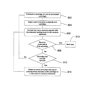
cartridge to the
receiver substrate. Here, during the first step 802, a cartridge is loaded (or
picked) or in another
embodiment, a spare equipment arm is pre-loaded with the cartridge. During the
second step
804, the cartridge is aligned with part (or all of) of the receiver substrate.
The alignment can be
done through using dedicated alignment mark on cartridge and the substrate, or
using the micro
devices and the landing are on the receiver substrate. the micro devices are
transferred to the
selected landing areas during the third steps. If the receiver substrate is
fully populated, the
substrate is moved to the next steps. If further population is needed, it goes
to further transfer
steps. Before a new transfer cycle, if the cartridge does not have enough
devices, the cycle start
from first step 802. if the cartridge has enough devices, the cartridge is
offset (or moved and
aligned) to a new area of the receiver substrate 814 and new cycle continous
to step 806. some of
these steps can be merged and/or rearranged.
[00139] FIG. 9 shows the steps of transferring the devices from the
cartridge to the
receiver substrate. Here, during the first step 902, a cartridge is loaded (or
picked) or in another
embodiment, a spare equipment arm is pre-loaded with the cartridge. During the
second step
902-2, a set of micro-devices is selected in cartridge that the number of
defects in them is less
than a threshold. During the third step 904, the cartridge is aligned with
part (or all of) of the
receiver substrate. The alignment can be done through using dedicated
alignment mark on
CA 2986503 2017-11-23
- 25 -
cartridge and the substrate, or using the micro devices and the landing are on
the receiver
substrate. The micro devices are transferred to the selected landing areas
during the third steps. If
the receiver substrate is fully populated, the substrate is moved to the next
steps. If further
population is needed, it goes to further transfer steps. Before a new transfer
cycle, if the cartridge
does not have enough devices, the cycle start from first step 902. if the
cartridge has enough
devices, the cartridge is offset (or moved and aligned) to a new area of the
receiver substrate
902-2.
[00140] FIG
10 shows an exemplary processing steps for developing multi-type micro
device cartridge. During the first step 1002, at least two different micro-
devices are prepared on
a difference substrates. During this step, the devices are formed and post
processing are
performed on the devices. During the second step 1004, the devices are
prepared to be separated
from the substrates. This step can involve securing the micro-devices by using
anchor or fillers.
During the third step 1006, the first devices are moved to the cartridge.
During the fourth step
1008, at least second micro devices are moved to the cartridge. In one case,
during this step, the
micro devices are bonded to the cartridge substrate through a bonding layer
directly or indirectly.
Then the micro devices are separated from the micro device substrates. In case
of direct transfer,
the different type of micro device can have different height to assist the
direct transfer. For
example, the second type of micro device that being transferred to the
cartridge can be slightly
taller than the first one (or the location on the cartridge can be slightly
higher for the second
micro device types). Here, after the cartridge is fully populated, the micro
device height can be
adjusted to make the surface of cartridge planar. This can be done either by
adding materials to
the shorter micro devices or by removing material from taller micro devices.
In another case, the
landing area on the receiver substrate can have different height associated
with the difference in
the cartridge. Another method of populating the cartridge is based on pick and
place. The micro
devices can be moved to the cartridge by means of pick-and-place process.
Here, the force
element on the pick-and-pance head can be unified for the micro devices in one
cluster in the
cartridge or it can be single for each micro devices. Also, they can be moved
to the cartridge with
other means. In another case, the extra devices are moved away from the
substrate of first or
second (third or other) micro devices and the other types of the micro devices
are transferred into
CA 2986503 2017-11-23
- 26 -
the empty areas. After the devices are secured on the cartridge substrate,
other processing steps
can be done such as adding filler layer, removing some layers, adding
electrical (e.g. contact) or
optical (lense, reflectors, ...) layers. The devices can be test after each
before being used to
populate the receiver substrate. The test can be electrical or optical or
combination of two. the
test can identify defects and/or performance of the devices on the cartridge.
The cartridge is
moved to the receiver substrate during the last step 1010 to transfer the
devices to the receiver
substrate. Some these steps can be rearranged or merged.
[00141] FIG 11 shows one example of multi-type micro-device cartridge.
This
cartridge includes three different micro devices 1102, 1104, 1106. It can have
more device types.
The distance between micro devices xl, x2,x3 are related to the pitch of the
landing areas in the
receiver substrate. After few devices which can be related to the pixel pitch
in the receiver
substrate, there can be a different pitch x4, y2. This pitch is to compensate
for mismatch between
the pixel pitch and micro device pitch (landing area pitch). In this case, if
pick and place is used
for developing the cartridge, the force elements can be in form of columns
corresponding to the
column of each micro device types or it can be separate element for each micro
device.
[00142] FIG 12 shows one example of multi-type micro-device cartridge.
This
cartridge includes three different micro devices 1202, 1204, 1206. The other
area 1206-2 can be
spare micro devices (It can have more device types. The distance between micro
devices xl,
x2,x3 are related to the pitch of the landing areas in the receiver substrate.
After few devices
which can be related to the pixel pitch in the receiver substrate, there can
be a different pitch x4,
y2. This pitch is to compensate for mismatch between the pixel pitch and micro
device pitch
(landing area pitch).
[00143] FIG 13 shows one example of micro devices 1302 prepared on
substrate
1304 before transferring to multi-type micro-device cartridge. Here, one can
use supporting
layers 1306 1308 for individual device or for a group of devices. Here, the
pitch can match the
pitch in the cartridge or it can be multiple of cartridge pitch.
[00144] In all the structures above, it is possible to move the micro
devices from the
first cartridge to a second one prior to using them in populating a substrate.
Extra processing step
CA 2986503 2017-11-23
- 27 -
can be done after transfer. or some of the the processing steps can be divided
between first and
secondary cartridge structure.
[00145] FIG 14A shows an example of microdevices in donor substrate
1480. The
microdevices can have gradual non-uniformity across the donor substrate. Since
the devices are
transferred in block 1482 into the receiver substrates, the adjacent devices
in the receiver
substrate where one block end and another one starts 1484 can result in abrupt
change as
demonstrated in FIG I4B. This change can result in visual artifact for
optoelectronic devices
such as displays. In one embodiment shown in FIG 14C, the edge of the blocks
are not sharp
lines and the devices are skewed. Therefore, the average impact of the sharp
transition is reduced
significantly. The skew can be random and can have different profiles. FIG.
14D shows another
embodiment where the microdevices in adjacent blocks are flipped so that the
devices with
similar performance are stay adjacent. This can keep the changes very smooth.
FIG. 14E shows
an exemplary combination of flipping the devices and skewing the edges to
improve the average
uniformity furthermore. Here, the examples shows the device non-uniformity in
one direction.
However, it can be in both directions so the methods described here can be
used in both
direction.
[00146] In one case, the performance of micro devices at the edges is
matched for
adjacent transferred block (array) prior to the transfer.
[00147] FIG 15A shows using two or more blocks 1582-1 1582-2, to
populate a
block in the receiver substrate. Here also the method of skewing or flipping
can be used for
further improving the average uniformity as demonstrated in FIG 15B. Also,
random or defined
pattern can be used to populate the cartridge with more than one block. FIG
16A shows a
samples with more than one blocks. The blocks can be from the same donor
substrate or different
donor substrates. FIG 16B shows an example of populating cartridge from
different blocks.
[00148] FIG 17 A and B show an structures with multiple cartridges
1790. Here, the
position of cartridges are chosen in away to eliminate overlapping the same
area in the receiver
substrate with cartridges with the same micro-devices during different
transfer cycle. In one case,
the cartridge can be independent which means separate arms or controller is
handling each
cartridge independently. In another case, the alignment can be done
independently, but the other
CA 2986503 2017-11-23
- 28 -
actions can be synchronized. In this case, the substrate can move to
facilitate the transfer after the
alignment. In another case, the cartridges move together to facilitate the
transfer after the
alignment. In another case, both can move to facilitate the transfer. In
another case, the cartridges
can be assembled in advanced. In this case, a frame or substrate can hold the
assembled
cartridges. The distance X3, Y3 between cartridge 1790 can be a multiple of
the width X 1, X2 or
length Y I, Y2 of the cartridge 1790. It can be a function of moving steps to
different direction.
For example, X3 = KX1+HX2, where K is the movement step to left (directly or
indirectly) and
II is the movement steps to the right (directly or indirectly) for populating
a substrate. The same
can be used for distance between cartridge Y3 and the length of Y1 and Y2. As
shown in FIG
17A, the cartridges can be aligned in one or two direction. In another case,
shown in FIG 17B,
the cartridges are not aligned in at least one direction. Each cartridge can
have independent
control for applying pressure and temperature toward the substrate. The Other
arrangement is
also possible depending on the direction of movement between substrate and
cartridges.
[00149] In
another case, the cartridges can have different devices and therefore
populating different areas in the receiver substrate with different devices.
In this case, relative
position of cartridges and receiver substrate changes after each transfer
cycle to populate
different area with all the required micro devices from different cartridges.
[00150] In
another case, several array of cartridges are prepared. Hereafter devices are
transferred to the receiver substrate from first array of cartridges, the
receiver is moved to the
next array of micro devices to fill the remaining areas in the receiver
substrate or receive
different devices.
[00151] In
another case, the cartridges can be on a curve surface and therefore
circular movement provide contact for transferring micro devices into
substrate.
[00152] The
process of micro devices generally starts by developing a stack of
crystalline layers on top of a substrate. Then by extra processing steps, the
stack of the films is
transformed into micro devices. In some cases, the substrate has different
crystalline lattice
compared to the crystal lattice of the stacked layers. In one case, a thick
buffer layer is deposited
first to masks the defects caused by the lattice mismatch. The main challenge
is that the buffer
CA 2986503 2017-11-23
- 29 -
layer is thick and therefore causes the cost goes high and the throughput to
drop. Moreover, the
buffer layer does not eliminate all the defects.
[00153] In one case, a sacrificial layer is used between buffer layer
and the stacked
layers. Therefore, instead of lifting off the stacked layers and the buffer
layers to transfer the
micro devices, the layers after the sacrificial layer are liftoff.
[00154] FIG 19 shows an embodiments using a template for transferring
multiple
cartridges to populate a system substrate with micro devices, here, the
template have more than
one cartridge, during first step 1902, at least one cartridge is aligned with
the template which has
some alignment mark facilitating the alignment process. During the second step
1904, at least
one cartridge is bonded to the template. The bonding mechanism could be
different forms such
as thermal, optical, vacuum, van der waals, etc. There can be a loop 1906,
that repeats the steps
1902, 1904 to bond more cartridges to the template. Then the template is
aligned with the
receiver substrate.
[00155] FIG 20 shows an example of a template transfer system. Here,
the template
2002, has multiple cartridges 2004 which can be loaded on a structure 2002-2.
The said structure
2002-2 can offer more rigidity and also a high profile. The height profile can
be controlled
independently for each structure 2002-2. The structure 2002-2 can be the same
size, smaller or
larger than the cartridge. This structure 2002-2 can be also a bonding
apparatus that assist the
transfer of microdevices from the cartridge 2004 into receiver substrate 2010.
The bonding
apparatus can provide pressure, temperature, optical, and other type of force
to assist the transfer.
In another case, the bonding apparatus 2006 is at the other side of the
template 2002. Also, some
support structure 2008 can hold the template in place. The support 2008 can be
at either side of
the template 2002. In one case, the support structure can be the same as the
bonding apparatus. In
another case, there is a separate bonding apparatus for each cartridge. In
another case, the
bonding apparatus is the same for at least more than one cartridges. The
receiver substrate 2010
also has support structures 2014, 2016. The support structure can be at either
side of the receiver
substrate. In one case, the receiver substrate may have bonding apparatus 2012
that can assist or
initiate the bonding process. Either bonding apparatus 2006 or 2012 can be
used for bonding.
The support structure 2014 can be the same as the receiver bonding apparatus
2012. In another
CA 2986503 2017-11-23
- 30 -
case, multiple template can be used to populate a receiver substrate. Here,
each template can be
aligned independently with the receiver substrate.
[00156] The support structure can be a suction apparatus, magnetic, a
spring loaded
pin, a gas bed made of pressured gas such as air or nitrogen, etc.
[00157] the area between cartridge 2004 and bonding apparatus 2006 on
the template
2002 can have different thermal and or mechanical property. In one case it can
be made of
different material with higher thermal conduction. In another case, vias may
form on template in
either different areas or at least in one of the area between the cartridge
2004 and apparatus 2006
and the other areas. The size of the VIAs can be adjusted for each area to
adjust the mechanical
property. In another case, the VIAs can be filed with different materials to
adjust the mechanical
and or thermal property of different areas of the template 2002,
[00158] The invention being thus described, it will be obvious that the
same may be
varied in many ways. Such variations are not to be regarded as a departure
from the scope of the
invention, and all such modifications as would be obvious to one skilled in
the art are intended to
be included within the scope of the following claims.
CA 2986503 2017-11-23