Note: Descriptions are shown in the official language in which they were submitted.
CA 02986831 2017-11-22
CHIP ASSEMBLY FOR MEASURING ELECTROCHEMICAL REACTION ON
SOLID-LIQUID PHASE INTERFACE IN SITU
Technical field
The present disclosure belongs to the technical field of scanning electron
microscopy test devices,
and more particularly, relates to a chip assembly for in-situ observation of
an electrochemical
reaction on a solid-liquid interface.
Background art
The study of solid-liquid interface, because of its importance in biology,
chemistry and interface
sciences, has always been a hotspot of scientific research worldwide. In
recent years, with the
rise of nano-material science, more and more research results show that the
nanostructure of a
material has a critical effect on its properties. Scanning electron microscope
(SEM) as a powerful
tool for characterizing the surface structure of a material can be used to
obtain the information
such as high resolution nanostructure, surface morphology change of a sample
and energy
spectrum of a chemical element through analysis. Moreover, the requirement of
SEM on the size
of a liquid chip/cell is much lower than that of transmission electron
microscope (TEM). The
chip size is not limited, facilitating the observation of morphology change of
the sample.
The current SEM solid-liquid interface test methods make use of the specially-
made
sample-holder-matched liquid chip/cell. Generally, two chips are packaged by
use of an epoxy
resin, wherein one chip provides a groove with four edges for holding the to-
be-tested liquid, the
other chip provides a silicon nitride membrane window, and then electrodes are
made on the two
chips through a micro fabrication process to achieve in-situ electrochemical
test on solid-liquid
interfaces in a SEM. However, there are two major drawbacks for the existing
in-situ SEM
electrochemical testing chip/cell: (1) the cost is very high; the customers
who use this technology
need to buy a specially-made sample holder which costs at least 100,000 RMBs
or more, thereby
1
CA 02986831 2017-11-22
greatly limiting the application of this technology; (2) the requirements on
the microfabrication
processing of the liquid chip/cell are very high; since this technology makes
use of a
specially-made sample holder to hold the liquid chip/cell, it is required that
the size and the
structure of the liquid chip/cell match with the sample holder.
Summary
In order to solve the above-mentioned problems of the related technics, the
present disclosure
provides a chip assembly for in-situ observation of an electrochemical
reaction on a solid-liquid
interface, which can be applied to the conventional SEM sample stage without
the use of a
specially-made sample holder, thereby significantly reducing the cost.
To achieve the above object of the present disclosure, the present disclosure
adopts the following
technical solution:
A chip assembly for in-situ observation of an electrochemical reaction on a
solid-liquid interface
comprises a first electrode, a second electrode, a first insulating film, a
second insulating film, a
third insulating film, a fourth insulating film as well as a top chip and a
bottom chip which are
oppositely arranged and of which two sides are correspondingly combined in a
sealing manner;
wherein the top chip has a through hole, the first insulating film covers the
inner surface of the
top chip and the opening of the through hole on the inner surface of the top
chip, and the second
insulating film covers the outer surface of the top chip; the first electrode
is disposed on the
surface of the first insulating film towards the bottom chip and located under
the through hole; a
part of the inner surface of the bottom chip is recessed to form a groove
opposite to the through
hole, the third insulating film covers the inner surface and the outer surface
of the bottom chip,
the fourth insulating film covers the inner wall of the groove and the third
insulating film on the
inner surface of the bottom chip; and the second electrode is disposed on the
fourth insulating
film and located on one side of the groove.
2
CA 02986831 2017-11-22
Further, the size of the through hole is gradually increasing in a direction
away from the inner
surface of the top chip.
Further, the first electrode has a grid structure.
Further, the size of the first electrode matches with the opening of the
through hole on the inner
surface of the top chip.
Further, the first electrode extends towards the side end of the top chip to
form a first electrode
extending portion.
Further, the chip assembly further comprises a first adhesive member and a
second adhesive
member, the first adhesive member being disposed between the second electrode
and the first
insulating film opposite to the second electrode, and the second adhesive
member being disposed
between the first electrode extending portion and the fourth insulating film
opposite to the first
electrode extending portion.
Further, the first adhesive member and/or the second adhesive member are
adhesives formed of
epoxy resin.
Further, the first insulating film and/or the second insulating film and/or
the third insulating film
and/or the fourth insulating film are formed of silicon nitride.
Further, the material of the first electrode and/or the second electrode is a
conductive metal.
Further, the sizes of the top chip and the bottom chip are from 1.5 cm x 2 cm
to 2 cm x 3 cm.
By making a large-size top chip and bottom chip with size in a range from 1.5
cm x 2 cm to 2 cm
x 3 cm, and making a first electrode and a second electrode through micro-
processing on the top
chip and bottom chip, respectively, the present disclosure provides a chip
assembly which can be
3
i
CA 02986831 2017-11-22
applied to the conventional SEM sample stage, thereby eliminating the need for
a specially-made
sample holder and greatly reducing the test cost (reducing from tens of
thousands RMBs to a few
thousand RMBs); meanwhile, the first electrode has a grid structure, which is
beneficial for
observing morphology change of the to-be-tested sample at the edge of the grid
structure.
Therefore, the chip assembly for in-situ observation of an electrochemical
reaction on a
solid-liquid interface according to the present disclosure not only
significantly reduces the test
costs, but also is beneficial for observing the change of the to-be-tested
sample.
Brief Description of the Drawings
The foregoing and other aspects, features and advantages of the embodiments of
the present
disclosure will become more apparent from the following description taken in
conjunction with
the accompanying drawings, in which in the drawings:
Figure 1 is a cross-sectional view of a chip assembly for in-situ observation
of an
electrochemical reaction on a solid-liquid interface according to an
embodiment of the present
disclosure;
Figure 2 is a top view of a first electrode according to an embodiment of the
present disclosure.
Detailed Description
Hereinafter, embodiments of the present disclosure will be described in detail
with reference to
the accompanying drawings. However, the present disclosure can be implemented
in many
different ways and the present disclosure should not be construed as being
limited to the specific
embodiments set forth herein. Rather, these embodiments are merely provided to
explain the
principles and its practical applications of the present disclosure so as to
enable others skilled in
the art to understand the various embodiments of the present disclosure and
various
modifications that are suitable for a particular intended application. In the
drawings, for the sake
4
CA 02986831 2017-11-22
of clarity, the shape and size of the elements can be exaggerated, and the
same reference
numerals will always be used to denote the same or similar elements.
It will be understood that although the terms "first" and "second" and the
like can be used herein
to describe various elements, these elements should not be limited by these
terms which are used
only to distinguish one element from another.
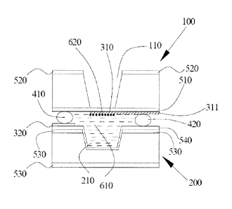
Figure 1 is a cross-sectional view of a chip assembly for in-situ observation
of an
electrochemical reaction on a solid-liquid interface according to an
embodiment of the present
disclosure.
Referring to Figure 1, the chip assembly for in-situ observation of an
electrochemical reaction on
a solid-liquid interface according to an embodiment of the present disclosure
comprise a top chip
100, a bottom chip 200, a first electrode 310, a second electrode 320, a first
adhesive member
410, a second adhesive member 420, a first insulating film 510, a second
insulating film 520, a
third insulating film 530, and a fourth insulating film 540; wherein the top
chip 100 and the
bottom chip 200 are oppositely arranged, and two sides of the top chip 100 and
the bottom chip
200 are correspondingly combined in a sealing manner by the first adhesive
member 410 and the
second adhesive member 420, respectively.
In this embodiment, the top chip 100 and the bottom chip 200 are made of a Si
wafer having a
size about 2 cm x 3 cm and a thickness of 200 pm. The material of the first
adhesive member
410 and the second adhesive member 420 is epoxy resin; wherein, the thickness
of the top chip
100 and the bottom chip 200 is not particularly limited and is generally
controlled within a range
of 200 m-500 p.m depending on the thickness of the specifically selected Si
wafer. The distance
between the top chip 100 and the bottom chip 200 is also not particularly
limited and depends on
the amount of the epoxy resin used when bonding. However, the present
disclosure is not limited
thereto, and the size of the top chip 100 and the bottom chip 200 are
generally controlled within
a range from 1.5 cm x 2 cm to 2 cm x 3 cm to satisfy the requirements of the
present disclosure.
CA 02986831 2017-11-22
In this way, an enclosed cavity is composed of the top chip 100, the bottom
chip 200, the first
adhesive member 410 and the second adhesive member 420, which can then be used
to
immobilize the to-be-tested liquid 610 when in-situ observation of the
electrochemical reaction
on solid-liquid interfaces.
Specifically, the top chip 100 has a through hole 110 throughout the top chip
100, and the size of
the through hole 110 is gradually increasing in a direction away from the
inner surface of the top
chip 100; that is, the through hole 110 is essentially a groove with four
edges, and its
cross-sectional shape is an inverted trapezoid.
The opening of the through hole 110 towards the bottom chip 200 and the inner
surface of the
top chip 100 are covered with a first insulating film 510, in this way, the
through hole 110 and
the first insulating film 510 covering the opening thereof form a viewing
window when in-situ
observation is performed; while the outer surface of the top chip 100 is
covered with a second
insulating film 520. Meanwhile, the first electrode 310 is located under the
through hole 110 and
is disposed on the surface of the first insulating film 510 towards the bottom
wafer 200, and the
first electrode 310 also extends towards the side end of the top chip 100 to
form a first electrode
extending portion 311.
More specifically, the size of the first electrode 310 corresponds to the size
of the opening of the
through hole 110 on the inner surface of the top chip 100, and the first
electrode 310 also has a
grid structure, as shown in Figure 2; when the in-situ SEM observation of the
electrochemical
reaction on a solid-liquid phase interface is performed, the to-be-tested
solid sample 620 is
placed to the grid structure where the to-be-tested solid sample 620 thus
contacts with the
to-be-tested liquid 610 in the enclosed cavity and reacts. It is convenient to
observe the
morphology change of the to-be-tested solid sample 620 occurring in the to-be-
tested liquid 610
due to such grid structure.
The bottom chip 200 comprises a groove 210 opposite to the through hole 110
formed by
6
CA 02986831 2017-11-22
recessing a part of the inner surface. The groove 210 in this embodiment also
presents a shape of
a groove with four edges; of course, the shape of the through hole 110 and the
shape of the
groove 210 are not changeless, and they can have other shapes with similar
functions, for
example, the groove 210 can also have other irregular shapes.
It is similar to the construction of the top chip 100 that the inner surface
of the bottom chip 200
located on both sides of the groove 210 and the outer surface of the bottom
chip 200 are covered
with a third insulating film 530, while the inner wall of the groove 210 and
the third insulating
film 530 on the inner surface of the bottom chip 200 are covered with a fourth
insulating film
540; and the second electrode 320 is directly disposed on the fourth
insulating film 530 located
on one side of the groove 210; that is, the inner surface of the bottom chip
200 is covered with a
third insulating film 530 and a fourth insulating film 540 sequentially.
Preferably, the material of the first insulating film 510, the second
insulating film 520, the third
insulating film 530 and the fourth insulating film 540 is a low stress silicon
nitride membrane,
and the stress of the low stress silicon nitride membrane is about 250 MPa. In
this embodiment,
the thicknesses of the first insulating film 510 and the second insulating
film 520 are both 50 nm,
and the thicknesses of the third insulating film 530 and the fourth insulating
film 540 are both 50
nm. Of course, the present disclosure is not limited thereto, as long as the
stress of the low stress
silicon nitride membrane used as the first insulating film 510, the second
insulating film 520, the
third insulating film 530 and the fourth insulating film 540 is controlled to
be not more than 250
MPa, and the thicknesses of the first insulating film 510 and the second
insulating film 520
located on the top chip 100 is controlled within a range of 50 nm-80 nm, and
the thickness of the
third insulating film 530 and the fourth insulating film 540 located on the
bottom chip 200 is
controlled within a range of 50 nm-200 nm.
In this embodiment, the first adhesive member 410 is disposed between the
second electrode 320
and the first insulating film 510 opposite thereto, and the second adhesive
member 420 is
7
CA 02986831 2017-11-22
disposed between the first electrode extending portion 311 and the fourth
insulating film 540
opposite thereto.
Further, the first adhesive member 410 and the second adhesive member 420 are
both adhesives
formed of epoxy resin. Of course, other adhesives which can achieve the
corresponding
combination in a sealing manner of both sides of the top chip 100 and the
bottom chip 200 can
also be used, and this technology is a common practice for those skilled in
the art and will not be
repeated any more here.
In this embodiment, it is preferable that the first electrode 310 is an Au
electrode and the second
electrode 320 is a Cu electrode. It is worth noting that both the first
electrode 310 and the second
electrode 320 are immersed in the to-be-tested liquid 610, and the to-be-
tested solid sample 620
is carried on the first electrode 310, and therefore it is required that
neither the first electrode 310
nor the second electrode 320 will react with the to-be-tested liquid 610 and
the to-be-tested solid
620. Of course, the first electrode 310 and the second electrode 320 are
generally guided out
through a conventional SEM hot stage and used for the electrochemical test,
thus it is only
required that they have conductive properties, that is, in the present
disclosure, the first electrode
310 and the second electrode 320 can be formed of other suitable types of
conductive metal or
other suitable types of conductive materials, the specific selection depends
on the types of the
to-be-tested liquid sample 610 and the to-be-tested solid sample 620 in the
actual operation.
The preparation process of the chip assembly which is suitable for in-situ SEM
observation of an
electrochemical reaction on a solid-liquid interface is as follows:
First, the preparation of the top chip 100 specifically adopts the following
method.
(1) A Si wafer having a thickness of 200 pm was selected as the material of
the top chip 100 and
a silicon nitride membrane (the stress of the silicon nitride membrane was
about 250 MPa) with a
thickness of 50 nm was grown on the opposite two sides of the Si wafer by
chemical vapor
8
CA 02986831 2017-11-22
deposition method.
(2) A region with a size of 1 cm x 1 cm was selected at the middle of the
silicon nitride
membrane on one side, the silicon nitride membrane at this region was removed
by use of
photolithography and plasma etching for 4 minutes, which was used as the
initial position for
making the through hole 110 in the top chip 100.
(3) The Si wafer was etched from the above selected initial position by a
potassium hydroxide
wet process until the silicon nitride membrane on the other side was exposed,
in this way, the
through hole 110 was formed, while the remaining silicon nitride membrane
covering the surface
of the Si wafer was the first insulating film 510 and the second insulating
film 520.
It is worth noting that during the etching of the Si wafer, the formed through
hole 110 was a
groove with four edges, that is, the cross-sectional shape of the through hole
110 was a
trapezoidal shape, so that the through hole 110 had two openings with
different sizes; wherein,
the silicon nitride membrane covering the smaller opening of the through hole
110 and the
surface of the top chip 100 extending towards both sides of the opening was
the first insulating
film 510, and the silicon nitride membrane covering the other surface of the
top chip 100 was the
second insulating film 520. During the subsequent assembly of the top chip 100
and the bottom
chip 200, the first insulating film 510 faced the bottom chip 200, that is,
the first insulating film
510 essentially covered the inner surface of the top chip 100 and the opening
of the through hole
110 on the inner surface of the top chip 100, and the second insulating film
520 covered the top
surface of the top chip 100.
(4) Metal Au with a thickness of 50 nm was deposited on the first insulating
film 510 between
the lower end of the through hole 110 and the side end of the top chip 100 by
using an electron
beam evaporation method to form the first electrode 310 and the first
electrode extending portion
311, and in the deposition process, the grid structure formed by
photolithography at a place
opposite to the through hole 110 allowed the first electrode 310 located under
the through hole
9
CA 02986831 2017-11-22
110 to have a grid structure, and the metal Au deposited by extending the
first electrode 310
towards the side end of the top chip 100 was the first electrode extending
portion 311. It is worth
noting that the first electrode 310 and the first electrode extending portion
311 were formed on
the surface of the first insulating film 510 towards the bottom chip 200.
Then, the preparation of the bottom chip 200 specifically adopts the following
method.
(5) Another Si wafer having a thickness of 200 [tm was selected as the
material of the bottom
chip 200 and a silicon nitride membrane (the stress of the silicon nitride
membrane was about
250 MPa) with a thickness of 50 nm was grown on the opposite two sides of the
Si wafer by
chemical vapor deposition method.
(6) The Si wafer was etched by the potassium hydroxide wet etching process
until a groove with
four edges having an opening size of 1 cm x 1 cm was formed as the groove 210
of the bottom
chip 200, wherein the etching depth was controlled to be about 100 um, i.e.,
the depth of the
groove 210 was about 100 um. In this way, the silicon nitride membrane on both
sides of the Si
wafer except for the groove 210 was the third insulating film 530.
(7) A silicon nitride membrane with a thickness of 50 nm was grown on the
inner wall of the
groove 210 and the third insulating film 530 on both sides of the groove 210
by the chemical
vapor deposition method as the fourth insulating film 540. That is, the fourth
insulating film 540
was arranged oppositely with respect to the first insulating film 510.
(8) Metal Cu with a thickness of 50 nm was deposited on the fourth insulating
film 540 on the
inner surface of the bottom chip 200 by the electron beam evaporation method
to form the
second electrode 320, wherein the second electrode 320 and the first electrode
310 were not at
the positions opposite to each other. That is, the second electrode 320 was
actually located on the
fourth insulating film 540 on one side of the groove 210.
CA 02986831 2017-11-22
It is worth noting that during the etching of the top chip 100 to make the
through hole 110 and
the etching of the bottom chip 200 to make the groove 210, the etching could
be completed
automatically by calculating the size of the initial etching position of the
through hole 110 and
the size of the etched opening of the groove 210 in advance, and then
considering the thickness
of the Si wafer used for the top chip 100 and the bottom chip 200, thereby
forming the through
hole 110 and the groove 210 with a predetermined size. That is, the sizes of
the through hole 110
and the groove 210 were related to the size of the initial etching position
and the size of the
etched opening, respectively. Meanwhile, the factors such as the thickness and
the stress of the
first insulating film 510 consisted of silicon nitride membrane located at the
opening on one side
of the through hole 110 also affected the design of the through hole 110. The
general method for
designing the size of the through hole 110 and the groove 210 comprises:
first, determining the
sizes of the regions at which the through hole 110 and groove 210 are etched
and the thicknesses
of the Si wafers selected for the top chip 100 and the bottom chip 200; then
etching along the
crystal orientation, such that the through hole 110 and the groove 210 with a
predetermined size
are formed.
The size of the top chip 100 and bottom chip 200 prepared as described above
were both 2 cm x
3 cm.
Finally, the to-be-tested solid sample 620 was adhered to the grid structure
of the first electrode
310, the to-be-tested liquid 610 was placed in the groove 210 of the bottom
chip 200, and two
opposite ends of the top chip 100 and the bottom chip 200 were bonded by using
an epoxy resin
as an adhesive to form the first adhesive member 410 and the second adhesive
member 420;
specifically, the first adhesive member 410 was disposed between the second
electrode 320 and
the first insulating film 510 opposite thereto, and the second adhesive member
420 was disposed
between the first electrode extending portion 311 and the fourth insulating
film 540 opposite
thereto; in this way, the to-be-tested solid sample 620 and the to-be-tested
liquid sample 610
were packaged in the enclosed cavity formed of the top chip 100, the bottom
chip 200, the first
11
CA 02986831 2017-11-22
adhesive member 410 and the second adhesive member 420, and then the first
electrode 310 and
the second electrode 320 could be guided out through a conventional SEM hot
stage and
subjected to the in-situ SEM observation of the electrochemical reaction on
the solid-liquid
interface.
The chips for in-situ observation of the electrochemical reaction on solid-
liquid interfaces
prepared by the above preparation method are used in the in-situ SEM test
without the use of
expensive specially-made sample holder, therefore the cost is significantly
reduced. Meanwhile,
the grid structure of the first electrode 310 disposed under the through hole
110 facilitates the
observation of the change of the to-be-tested sample.
While the present disclosure has been shown and described with reference to
specific
embodiments, it will be understood by those skilled in the art that various
changes in the form
and details may be made herein without departing from the spirit and scope of
the present
disclosure as defined by the appended claims and their equivalents.
12