Note: Descriptions are shown in the official language in which they were submitted.
CA 02987250 2017-11-24
WO 2016/196707
PCT/1JS2016/035374
SOLAR JUNCTION BOX FOR SOLAR PANEL
[0001] The subject matter herein relates generally to solar junction
boxes for solar panels.
[0002] Photovoltaic (PV) modules or arrays, such as solar panels,
produce electricity from solar energy. Electrical power produced by PV modules
reduces the amount of energy required from non-renewable resources such as
fossil
fuels and nuclear energy. Significant environmental benefits are also realized
from
solar energy production, for example, reduction in air pollution from burning
fossil
fuels, reduction in water and land use from power generation plants, and
reduction in
the storage of waste byproducts. Solar energy produces no noise, and has few
moving
components. Because of their reliability, PV modules also reduce the cost of
residential and commercial power to consumers.
[0003] PV cells are essentially large-area semiconductor diodes.
Due to the photovoltaic effect, the energy of photons is converted into
electrical
power within a PV cell when the PV cell is irradiated by a light source such
as
sunlight. PV cells are typically interconnected into solar modules that have
power
ranges of up to 100 watts or greater. For large PV systems, special PV modules
are
produced with typical power range of up to several 100 W. A photovoltaic
module is
the basic element of a photovoltaic power generation system. A PV module has
many
solar cells interconnected in series or parallel, according to the desired
voltage and
current parameters. PV cells are connected in series and placed between a back
sheet
on the bottom and a glass layer on the top. PV cells are interconnected with
thin
contacts, such as a foil, on the semiconductor layer. The foil is terminated
to a
junction box, which may electrically connect groups of the PV cells and/or
solar
panels.
[0004] The junction box is typically connected to the back side of the
solar panel, such as to the back sheet. The foil exits the semiconductor layer
and is
terminated to a corresponding terminal in the junction box. However, sealing
of the
-1-
84112960
junction box and/or foil are problematic. Additionally, the junction box may
block some of
the light, reducing the efficiency of the PV module. For example, some PV
modules are
bifacial panels where reflected sunlight is collected at the backside. Such
bifacial panels use a
glass layer as the back sheet (e.g., dual glass layer panel) to allow the
sunlight to pass through
the back sheet to the PV cells at the semiconductor layer. The junction box
blocks the
reflected sunlight at the backside. Additionally, it is costly to route the
foil through the glass
layer at the backside, such as by drilling a hole or slot in the glass layer.
At least some known
PV modules exit the foil at the edge of the solar panel. Heretofore,
terminating junction boxes
at such locations has proven problematic. For example, portions of the foil
are exposed and
susceptible to damage and water ingress. Additionally, the glass panels may
have various
thicknesses and thus no universal solution has been provided for terminating
junction boxes to
such solar panels.
[0005] The solution is provided by a solar junction box for a solar panel
having a semiconductor layer including at least one photovoltaic cell and a
foil electrically
connected to the at least one cell, the solar panel having a glass layer above
the semiconductor
layer and a back sheet below the semiconductor layer. The solar junction box
includes a
housing having walls defining a cavity. The housing is configured to be
mounted at an edge of
the solar panel. A terminal is received in the cavity and is configured to be
terminated to the
foil. An edge flap extends from the housing. The edge flap has an edge seal
configured to be
applied to the edge of the solar panel to seal the foil at the edge of the
solar panel.
[0005a] According to one aspect of the present invention, there is provided a
solar junction box for a solar panel having a semiconductor layer including at
least one
photovoltaic cell and a foil electrically connected to the at least one cell,
the solar panel
having a glass layer above the semiconductor layer and a back sheet below the
semiconductor
layer, the solar junction box comprising: a housing having a base, a first
side wall extending
from the base and end walls extending from the base at opposite ends of the
first side wall, the
base, first side wall and the end walls defining a cavity, the base of the
housing being
configured to be mounted at the back sheet proximate to an edge of the solar
panel such that
the first side wall is generally aligned along the edge of the solar panel; a
terminal received in
the cavity, the terminal being configured to be terminated to the foil; and an
edge flap
2
CA 2987250 2020-04-01
84112960
pivotably coupled to the housing at the first side wall, the edge flap
extending the length of
the side wall between the end walls and extending from the housing to wrap
around the edge
of the solar panel to the glass layer of the solar panel, the edge flap having
an edge seal
configured to be applied to the edge of the solar panel when the edge flap is
pivoted against
the edge of the solar panel to seal the foil at the edge of the solar panel.
[0005b] According to another aspect of the present invention, there is
provided a solar junction box for a solar panel having a semiconductor layer
including at least
one photovoltaic cell and a foil electrically connected to the at least one
cell, the solar panel
having a glass layer above the semiconductor layer and a back sheet below the
semiconductor
layer, the solar junction box comprising: a housing having a base, side walls
and end walls
defining a cavity, the base of the housing being configured to be mounted to
the back sheet at
an edge of the solar panel near a foil exit where the foil exits the solar
cell from between the
glass layer and the back sheet such that one of the side walls is generally
aligned along the
edge of the solar panel, the base configured to extend along and seal against
the back sheet; a
terminal received in the cavity, the terminal being configured to be
terminated to the foil; and
an edge flap pivotably coupled to the housing at one of the side walls, the
edge flap extending
the length of the corresponding side wall between the end walls and extending
from the
housing to wrap around the edge of the solar panel to the glass layer of the
solar panel, the
edge flap having a side wall and an end wall oriented generally perpendicular
to the side wall,
the side wall configured to extend along and seal against the edge of the
solar panel, the end
wall configured to extend along and seal against the glass layer, the edge
flap having an edge
seal configured to be applied to the edge of the solar panel at the foil exit
to seal the foil at the
edge of the solar panel.
[0005c] According to still another aspect of the present invention, there is
provided a photovoltaic system comprising: a solar panel having a
semiconductor layer
including at least one photovoltaic cell and a foil electrically connected to
the at least one cell,
the solar panel having a glass layer above the semiconductor layer and a back
sheet below the
semiconductor layer, the solar panel having an edge, the foil exiting the edge
at a foil exit; and
a solar junction box comprising: a housing having side walls and end walls
defining a cavity,
the housing being mounted to the solar panel at the edge near the foil exit
such that one of the
2a
CA 2987250 2020-04-01
84112960
side walls is generally aligned along the edge of the solar panel; a terminal
received in the
cavity, the terminal being terminated to the foil; and an edge flap pivotably
coupled to the
housing at one of the side walls, the edge flap extending the length of the
corresponding side
wall between the end walls and extending from the housing to wrap around the
edge of the
solar panel to the glass layer of the solar panel, the edge flap having an
edge seal applied to
the edge of the solar panel to seal the foil at the foil exit.
[0006] The invention will now be described by way of example with
reference to the accompanying drawings in which:
[0007] Figure 1 illustrates a photovoltaic (PV) system formed in accordance
with an exemplary embodiment.
[0008]
Figure 2 is a partially exploded view of a solar junction box of the
PV system formed in accordance with an exemplary embodiment
2b
CA 2987250 2020-04-01
CA 02987250 2017-11-24
WO 2016/196707
PCT/1JS2016/035374
poom Figure 3 illustrates the PV system showing the solar junction
box poised for mounting to a solar panel of the PV system.
[0010] Figure 4 illustrates a portion of the PV system showing the
solar junction box mounted to the solar panel with an edge flap of the solar
junction
box in an open position.
[0011] Figure 5 is another view of the PV system showing the edge
flap in a partially closed position.
[0012] Figure 6 is another view of the PV system showing the edge
flap in a closed position.
[0013] In one embodiment, a solar junction box is provided for a
solar panel having a semiconductor layer including at least one photovoltaic
cell and a
foil electrically connected to the at least one cell, the solar panel having a
glass layer
above the semiconductor layer and a back sheet below the semiconductor layer.
The
solar junction box includes a housing having walls defining a cavity. The
housing is
configured to be mounted at an edge of the solar panel. A terminal is received
in the
cavity and is configured to be terminated to the foil. An edge flap extends
from the
housing. The edge flap has an edge seal configured to be applied to the edge
of the
solar panel to seal the foil at the edge of the solar panel.
[0014] In another embodiment, a solar junction box is provided for a
solar panel having a semiconductor layer including at least one photovoltaic
cell and a
foil electrically connected to the at least one cell, the solar panel having a
glass layer
above the semiconductor layer and a back sheet below the semiconductor layer.
The
solar junction box includes a housing having side walls and end walls defining
a
cavity. The housing is configured to be mounted to the back sheet at an edge
of the
solar panel near a foil exit where the foil exits the solar cell from between
the glass
layer and the back sheet. A terminal is received in the cavity that is
configured to be
terminated to the foil. An edge flap extends from the housing. The edge flap
has a
side wall and an end wall oriented generally perpendicular to the side wall.
The side
-3-
CA 02987250 2017-11-24
WO 2016/196707
PCT/1JS2016/035374
wall extends along and seal against the edge of the solar panel and the end
wall
extends along and seals against the glass layer. The edge flap has an edge
seal
configured to be applied to the edge of the solar panel at the foil exit to
seal the foil at
the edge of the solar panel.
100151 In a further embodiment, a photovoltaic system is provided
including a solar panel having a semiconductor layer including at least one
photovoltaic cell and a foil electrically connected to the at least one cell.
The solar
panel has a glass layer above the semiconductor layer and a back sheet below
the
semiconductor layer. The solar panel has an edge and the foil exits the edge
at a foil
exit. The photovoltaic system also includes a solar junction box coupled to
the solar
panel. The solar junction box includes a housing having side walls and end
walls
defining a cavity. The housing is mounted to the solar panel at the edge near
the foil
exit. A terminal is received in the cavity and is terminated to the foil. An
edge flap
extends from the housing. The edge flap has an edge seal applied to the edge
of the
solar panel to seal the foil at the foil exit.
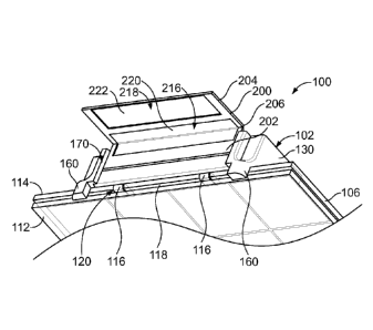
10016] Figure 1 illustrates a photovoltaic (PV) system 100 formed in
accordance with an exemplary embodiment. The PV system 100 includes one or
more solar junction boxes 102 (one shown in Figure 1), which may be
electrically
connected by connector assemblies 104 (e.g., cable connector assemblies). The
PV
system 100 includes a plurality of PV components 106. In an exemplary
embodiment, the PV components 106 may be any type of PV components, such as PV
modules or arrays that are used to generate electricity, such as solar panels,
or other
PV components used within the PV system 100 such as power storage devices,
sensors, controllers, and the like. In the illustrated embodiment, the PV
components
106 are solar panels and may be referred to hereinafter as solar panels 106.
The solar
panels 106 have a plurality of PV cells 108 configured to generate
electricity.
[0017] The connector assemblies 104 may be coupled solar junction
boxes 102 of the same solar panel 106 or solar junction boxes 102 of different
solar
-4-
CA 02987250 2017-11-24
WO 2016/196707
PCT/1JS2016/035374
panels 106. The connector assemblies 104 transmit power andJor data along the
transmission path between the PV components 106.
[0018] In an exemplary embodiment, the solar panel 106 includes a
semiconductor layer 110 sandwiched between a glass layer 112 and a back sheet
114.
The glass layer 112 may define a top layer of the solar panel 106 and the back
sheet
114 may define a bottom layer of the solar panel 106. The semiconductor layer
110
includes the cells 108 and conductors, such as conductive foils 116,
connecting the
cells 108 in series. Optionally, one or more EVA layers (e.g., thermoplastic
containing ethylene vinyl acetate) may be used, such as a layer used to
encapsulate
the PV cells 108. The foils 116 may he bus ribbons electrically connecting the
cells
and the solar junction box 102. Groups of the cells 108 may be electrically
connected
to the corresponding solar junction box 102. For example, the foil 116 may be
terminated to a corresponding terminal in the solar junction box 102. In an
exemplary
embodiment, the solar junction box 102 is mounted to the solar panel 106 at an
edge
118 of the solar panel 106. The foils 116 may extend from the edge to the
solar
junction box 102.
[0019] The glass layer 112 is positioned above the semiconductor
layer 110 and allows sunlight to pass therethrough to the cells 108. The back
sheet
114 is positioned below the semiconductor layer 110. The back sheet 114 may be
a
plastic layer. Alternatively, the back sheet 114 may be manufactured from
another
material. For example, the back sheet 114 may be another glass layer. For
example,
in some various embodiments, the solar panel 106 may be a bifocal solar panel
configured to receive sunlight from both sides of the solar panel 106. For
example,
the backside (back sheet 114) may receive reflective sunlight. The foils 116
from the
semiconductor layer 110 exit the solar panel 106 at foil exits 120 at the edge
118. The
foil exits 120 are between the glass layer 112 and the back sheet 114. The
foils 116
are routed to the solar junction box 102, which, in the illustrated
embodiment, is
mounted to the backside of the solar panel 106, such as to the back sheet 114.
-5-
CA 02987250 2017-11-24
WO 2016/196707
PCT/1JS2016/035374
[0020] The solar junction box 102 includes an edge flap 200 (shown
in an open position in Figure 1) used to cover and seal the foils 116. The
edge flap
200 accommodates various thicknesses of the solar panel 106. While Figure 1 is
a
bottom perspective view showing the solar junction box 102 mounted to the back
sheet 114, in use, the glass layer 112 would be on top or upward facing to
face the sun
and the solar junction box 102 would be mounted to the backside of the solar
panel
106. Other orientations are possible and terms denoting orientation (e.g.,
top, bottom,
up, down, etc.) may be relative to the orientation shown in the particular
Figure as
opposed to an orientation in use.
100211 Figure 2 is a partially exploded view of the solar junction box
102 formed in accordance with an exemplary embodiment. The solar junction box
102 includes a housing 130 configured to be mounted to the solar panel 106.
The
housing 130 includes a base 132 and a plurality of walls 134 extending from
the base
132. Any number of walls 134 may be provided to provide an appropriate shaped
housing for the particular application. In the illustrated embodiment, the
walls 134
include side walls 136 and end walls 138 extending between the side walls 136.
Optionally, the housing 130 may have a rectangular cross section, being long
and
narrow, with the side walls 136 longer than the end walls 138. Other shapes
are
possible in alternative embodiments.
100221 The side walls 136 and end walls 138 define a cavity 140 of
the housing 130. The solar junction box 102 also includes a lid or cover 142.
The
solar junction box 102 holds electrical components configured to be
electrically
connected to one or more of the foils 116 in the cavity 140. The cover 142
covers the
cavity 140 and electrical components. In an exemplary embodiment, the solar
junction box 102 includes a positive terminal 150 and a negative terminal 152
in the
cavity 140. In an exemplary embodiment, the solar junction box 102 includes a
bypass diode 154 between the terminals 150, 152. The solar junction box 102
may
include other electrical components in alternative embodiments. The positive
terminal 150 is terminated to a corresponding foil 116 and the negative
terminal 152
-6-
CA 02987250 2017-11-24
WO 2016/196707
PCT/1JS2016/035374
is terminated to a corresponding foil 116. The terminals 150 and/or 152 may be
terminated to other components, such as electrical connectors or cables.
[0023] In an exemplary embodiment, the solar junction box 102
includes edge alignment features 160 extending from the base 132. The edge
alignment features 160 may be provided at one of the side walls 136. The edge
alignment features 160 are configured to engage the edge 118 (shown in Figure
1) of
the solar panel 106 to align the solar junction box 102 at the edge 118 of the
solar
panel 106. In the illustrated embodiment, the edge alignment features 160 are
tabs or
posts extending from the base 132. A pair of the edge alignment features 160
are
provided each being at or near opposite end walls 138. Any number of edge
alignment features 160 may be provided in alternative embodiments.
[0024] In an exemplary embodiment, the solar junction box 102
includes a track 170 along one of the side walls 136 (e.g., the same side wall
136
having the edge alignment features 160). The track 170 receives the edge flap
200.
The track 170 may be open at the top opposite the base 132. Optionally, the
track 170
is defined by a pair of rails 172 at opposite sides of the track 170. The
rails 172 may
be provided at the end walls 138. The rails 172 faun slots 174 along the
corresponding side wall 136. Optionally, the solar junction box 102 may have a
retainer 176 at or near the top. The retainer 176 may hold the edge flap 200
in the
track 170. The edge flap 200 rides vertically up and down within the track 170
and
the retainer 176 may ensure that the edge flap 200 is held in the track 170.
The track
170 may be closed at the bottom or base of the track 170.
[0025] The edge flap 200 is used to cover the edge 118 of the solar
panel 106. The edge flap 200 is used to seal the foils 116 at the
corresponding foil
exits 120 (both shown in Figure 1). In an exemplary embodiment, the edge flap
200
includes a side wall 202 and an end wall 204 meeting at a corner 206.
Optionally, the
end wall 204 may be generally perpendicular with respect to the side wall 202.
The
edge flap 200 includes an interior 210 configured to face the solar panel 106
in an
exterior 212 opposite the interior 210.
-7-
CA 02987250 2017-11-24
WO 2016/196707
PCT/1JS2016/035374
[0026] In an exemplary embodiment, the edge flap 200 includes pins
214 extending from the side wall 202. Optionally, the pins 214 may be located
at
opposite edges of the side wall 202. The pins 214 are configured to be
received in
corresponding rails 172 of the track 170. In an exemplary embodiment, the pins
214
may ride along the rails 172 within the track 170. As such, the edge flap 200
is
configured to be slidably coupled to the housing 130 within the track 170. In
an
exemplary embodiment, the edge flap 200 is rotatable about the pins 214 within
the
track 170. As such, the edge flap 200 may be rotated relative to the housing
130.
[0027] In an exemplary embodiment, the edge flap 200 includes one
or more recesses 216 formed in the interior 210. For example, the edge flap
200
includes a recess 216 along the side wall 202 and/or along the end wall 204.
For
example, the first recess 216 may span across the corner 206 from the side
wall 202 to
the end wall 204. The edge flap 200 may include a second recess 218 in the end
wall
204. The first recess 216 is configured to receive an edge seal 220 that may
seal the
edge flap 200 to the edge 118 of the solar panel 106. Optionally, the edge
seal 220
may be a silicon sealant applied to the recess 216. Other types of edge seals
may be
provided in alternative embodiments, such as epoxy, a gasket, or another type
of
sealer. In an exemplary embodiment, adhesive tape 222, such as double sided
tape,
may be provided in the second recess 218. The tape 222 may be used to
initially hold
the edge flap 200 in a closed position against the solar panel 106 until the
edge seal
220 can be applied and sealed against the solar panel 106.
[0028] Figure 3 illustrates the PV system 100 showing the solar
junction box 102 poised for mounting to the solar panel 106. The foils 116
exit the
solar panel 106 at the edge 118 at foil exits 120. The foils 116 are wrapped
along the
edge 118 around the back sheet 114. The foils 116 extend along the outer
surface of
the back sheet 114 and are bent away from the solar panel 106 for loading into
the
solar junction box 102 when the solar junction box 102 is mounted to the solar
panel
106. The solar junction box 102 includes a base seal 230 applied to the base
132 of
the housing 130. The base seal 230 is used to mount the solar junction box 102
to the
-8-
CA 02987250 2017-11-24
WO 2016/196707
PCT/1JS2016/035374
solar panel 106. For example, the foils 116 may pass through foil openings in
the
solar junction box 102.
[0029] The base seal 230 seals the base 132 to the outer surface of
the back sheet 114. Optionally, the base seal 230 may be a silicon adhesive.
The base
seal 230 may be received in a pocket in the base 132. Optionally, adhesive
tape, such
as double sided tape may be applied to the base 132 to hold the solar junction
box 102
in place on the solar panel 106 while the base seal 230 cures or sets.
[0030] Figure 4 illustrates a portion of the PV system 100 showing
the solar junction box 102 mounted to the solar panel 106. Figure 4
illustrates the
edge flap 200 in an open position. Figure 5 is another view of the PV system
100
showing the edge flap 200 in a partially closed position. Figure 6 is another
view of
the PV system 100 showing the edge flap 200 in a closed position. The solar
junction
box 102 is coupled to the solar panel 106 at or near the edge 118. The edge
alignment
features 160 engage the edge 118 of the solar panel 106 to align the solar
junction box
102 with the solar panel 106. The solar junction box 102 covers the foils 116
where
the foils 116 extend along the back sheet 114. The foils 116 may be routed
into the
solar junction box 102 for electrical termination therein.
[0031] During assembly, the edge flap 200 is initially held in the
open position (Figure 4). The edge seal 220 may be applied to the edge flap
200, such
as in the recess 216. The edge seal 220 is applied in an area that will seal
the edge
flap 200 to the edge 118 and to the foils 116 at the foil exit 120.
Optionally, the tape
222 may be applied to the edge flap 200, such as in the recess 218. The liner
on the
tape 222 may be peeled back to ready the edge flap 200 for attachment to the
solar
panel 106.
[0032] The edge flap 200 is slida.bly received in the track 170 and is
rotatable relative to the housing 130. As the edge flap 200 is closed, the
edge flap 200
may be rotated in a closing direction (Figure 5). The edge flap 200 is rotated
around
the edge 118 of the solar panel_ 106 such that the end wall 204 wraps around
the edge
118 and is positioned along the glass layer 112. The edge flap 200 may be
rotated
-9-
CA 02987250 2017-11-24
WO 2016/196707
PCT/1JS2016/035374
closed until the side wall 202 abuts against the edge 118 of the solar panel
106. The
side wall 202 covers the edge 118 and the foils 116 at the foil exit 120 in
the closed
position. 'the side wall 202 covers the foils 116 as the foils 116 extend
along the edge
of the back sheet 114. The edge seal 220 may seal the foils 116 to protect the
foils
116 from environmental degradation, such as from water.
[0033] Once the edge flap 200 is rotated to a generally closed
position (Figure 6) with the sidewall 202 abutting against the solar panel
106, the
edge flap 200 may be pushed closed by pushing the end wall 204 against the
glass
layer 112. The edge flap 200 is slidable within the track 170 and may be slid
until the
end wall 204 abuts against the exterior of the glass layer 112. The corner 206
spans
the comer of the glass layer 112. The edge seal 220 at the end wall 204 is
pressed
against the glass layer 112. The tape 222 initially holds the edge flap 200 in
place in
the closed position. The tape 222 temporarily holds the edge flap 200 until
the edge
seal 220 cures or sets. Once the edge seal 220 cures, the edge seal 220
permanently
holds the edge flap 200 in place on the solar panel 106. The edge seal 220
provides a
permanent mechanical connection for the edge flap 200 to the solar panel 106.
The
edge seal 220 also seals the edge 118 and the foils 116.
-10-