Note: Descriptions are shown in the official language in which they were submitted.
CA 02987368 2017-11-27
1
DESCRIPTION
POWER CONVERSION DEVICE
TECHNICAL FIELD
[0001]
The present invention relates to a power conversion device for converting a
battery's DC power into AC power or converting the voltage of DC power.
BACKGROUND ART
[0002]
Automotive power electronics systems for use in electric cars and hybrid cars
are mainly constituted of a battery that supplies DC power, an inverter that
performs
DC-to-AC conversion, and a motor that obtains drive force from the electrical
output of
the inverter. The inverter in this case is a power conversion device.
[0003]
The power conversion device incorporates switches formed of power
semiconductor elements and, in the case of an inverter, converts DC power into
AC
power by opening and closing the switches and, in the case of a converter,
converts the
voltage by opening and closing the switches.
[0004]
There are cases where the voltage fluctuation resulting from the opening and
closing of the switches is radiated as a common mode noise and adversely
affects the
listening of the in-vehicle radio and other digital instruments. To solve
this, in a
conventional practice, a line that supplies power to the power conversion
device and a
grounding surface are connected by a capacitor to discharge the common mode
noise to
the ground potential (Patent Literature 1, for example).
CITATION LIST
PATENT LITERATURE
[0005]
Patent Literature 1: Japanese Patent Application Publication No. 2004-7888
SUMMARY OF INVENTION
TECHNICAL PROBLEM
CA 02987368 2017-11-27
2
[0006]
However, there are cases where the common mode noise discharged to the
ground potential leaks to the power conversion device's housing. This leads to
a
problem in that the channel through which the common mode noise leaks to the
housing
acts as an antenna, radiating unnecessary electromagnetic waves (radiation
noise), and
this radiation causes malfunction of other devices such as the in-vehicle
radio.
[0007]
The present invention has been made in view of the above problem, and an
object thereof is to provide a power conversion device that allows reduction
of the
common mode noise leaking to its housing.
SOLUTION TO PROBLEM
[0008]
A power conversion device according to one aspect of the present invention
includes a first power-supply busbar, a second power-supply busbar, a
switching
element, a first capacitor, a second capacitor, a grounding member, and a
conductive
member. The first power-supply busbar is arranged from the positive electrode
side of
a power source, the second power-supply busbar is arranged from the negative
electrode
side of the power source, and the switching element is provided between the
first
power-supply busbar and the second power-supply busbar. One end of the first
capacitor is connected to the first power-supply busbar, and one end of the
second
capacitor is connected to the second power-supply busbar. The grounding member
is
connected between the opposite end of the first capacitor and the opposite end
of the
second capacitor. Moreover, in the power conversion device according to the
present
invention, the conductive member is routed along at least one of the first
power-supply
busbar and the second power-supply busbar and connected between the grounding
member and a ground potential.
BRIEF DESCRIPTION OF DRAWINGS
[0009]
[Fig. 1] Fig. 1 is a diagram illustrating an example of the configuration of a
power
conversion device 1 in a first embodiment.
CA 02987368 2017-11-27
3
[Fig. 2] Fig. 2 is a diagram depicting the power conversion device 1 with
circuit
symbols.
[Fig. 3] Fig. 3 is a diagram explaining a stray capacitor Cp,,,2 in the power
conversion
device 1.
[Fig. 4] Fig. 4 is a graph illustrating examples compared with each other in
common
mode noise.
[Fig. 5] Fig. 5 is a diagram illustrating an example of the configuration of a
power
conversion device 2, which is the power conversion device 1 modified into a
converter.
[Fig. 6] Fig. 6 is a diagram illustrating an example of the configuration of a
power
conversion device 3 in a second embodiment.
[Fig. 7] Fig. 7 is a diagram depicting the power conversion device 3 with
circuit
symbols.
[Fig. 8] Fig. 8 is a diagram illustrating an example of the configuration of a
power
conversion device 4 in a third embodiment.
[Fig. 9] Part (a) of Fig. 9 illustrates the dimensions of two plate-shaped
conductive
bodies while part (b) of Fig. 9 is a graph illustrating tendencies of change
in mutual
inductance M with respect to these dimensions.
[Fig. 10] Fig. 10 is a diagram illustrating an example of the configuration of
a power
conversion device 5 in a fourth embodiment.
[Fig. 11] Fig. 11 is a diagram illustrating another example of the
configuration of the
power conversion device 5 in the fourth embodiment.
[Fig. 12] Fig. 12 is a cross-sectional view illustrating an example of the
relation
between a conductive member 14, a first power-supply busbar 10, and a second
power-supply busbar 11 in their routed state.
[Fig. 13] Fig. 13 is a graph illustrating the relation between balance CLBAL
in electrical
properties between the conductive lines (10, 11, 14) in Fig. 11 and the noise
intensity of
common mode noise.
[Fig. 14] Fig. 14 is a diagram illustrating an example of the configuration of
a power
conversion device 6 in a fifth embodiment.
[Fig. 15] Fig. 15 is a cross-sectional view illustrating an example of the
relation
CA 02987368 2017-11-27
4
between conductive members 14a, 14b, the first power-supply busbar 10, and the
second power-supply busbar 11 in their routed state.
[Fig. 16] Fig. 16 is a cross-sectional view illustrating another example of
the relation
between the conductive members 14a, 14b, the first power-supply busbar 10, and
the
second power-supply busbar 11 in their routed state.
[Fig. 17] Fig. 17 is a diagram illustrating an example of the configuration of
a power
conversion device 7 in a sixth embodiment.
[Fig. 18] Fig. 18 is a set of diagrams explaining an operation and
advantageous effect
achieved by setting the length of the conductive member 14 to X/4 of a
wavelength ?k, of
a high-frequency signal with a common mode voltage (current).
DESCRIPTION OF EMBODIMENTS
[0010]
Embodiments will be described with reference to the drawings. Identical
portions in the illustration of the drawings will be denoted by identical
reference signs,
and description thereof will be omitted.
[0011]
[First Embodiment]
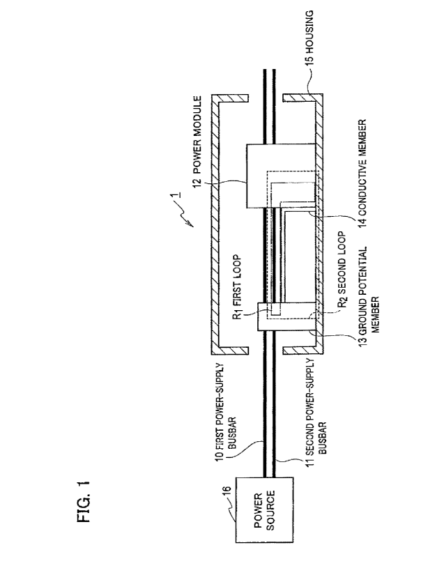
An example of the configuration of a power conversion device 1 in a first
embodiment is illustrated in Fig. 1. The power conversion device 1 in this
embodiment will be discussed with an example of an inverter that converts a
battery's
DC power into AC power in, for example, an automotive power electronics
system.
[0012]
The power conversion device 1 includes a first power-supply busbar 10, a
second power-supply busbar 11, a power module 12 (switching element), a ground
potential member 13, and a housing 15.
[0013]
The first power-supply busbar 10 supplies the power conversion device 1 with
a positive power source (positive electrode side) of a power source 16
(battery) that
supplies DC power. The second power-supply busbar 11 supplies the power
conversion device 1 with a negative power source (negative electrode side) of
the power
CA 02987368 2017-11-27
source 16. The first power-supply busbar 10 and the second power-supply busbar
11
can be arranged from any part of a power supply system.
[0014]
The power module 12 is provided between the first power-supply busbar 10
and the second power-supply busbar 11 and is supplied with DC power from the
power
source 16. The power module 12 is, for example, an inverter that converts the
DC
power into AC power by repetitively opening and closing switches therein by
means of
a control signal, illustration of which is omitted.
[0015]
The ground potential member 13 connects each of the first power-supply
busbar 10 and the second power-supply busbar 11 and the housing 15, which is
connected to a ground potential. This connection means an AC connection
through
reactance. Details will be described later.
[0016]
A conductive member 14 is routed along at least one of the first power-supply
busbar 10 and the second power-supply busbar 11 and connects the ground
potential
member 13 and the housing 15 near the power module 12. Thus, the first
power-supply busbar 10 and the second power-supply busbar 11 are connected to
the
ground potential by the ground potential member 13 and the conductive member
14.
[0017]
Here, being "routed along" means that the conductive member 14 is extended
by the side of at least one of the first power-supply busbar 10 and the second
power-supply busbar 11, each of which is extended in the shape of a line,
without
leaving a large gap therebetween over a certain length. A specific example
will be
described later.
[0018]
Now, common mode noise will be briefly described. The common mode
noise is defined as a noise that propagates through lines inside a device in a
common
manner, a noises that propagates through a ground potential surface (grounded
surface),
or the like. More specifically, the common mode noise is a noise generated
when the
CA 02987368 2017-11-27
6
switching elements in the power module 12 are connected and disconnected, and
flows
through the first power-supply busbar 10 and the second power-supply busbar 11
in the
same direction.
[0019]
In the power conversion device 1, when the switches in the power module 12
are opened and closed, a common mode current flow which charges and discharges
a
stray capacitor between an output node of the power module 12, illustration of
which is
omitted in Fig. 1, and the ground potential. That common mode current flows
through
the first power-supply busbar 10 and the second power-supply busbar 11
simultaneously
and flows through two channels--a first loop R1 (dashed-dotted line) running
through
the conductive member 14 and a second loop R2 (broken line) running through
the
housing 15.
[0020]
The larger the stray capacitor between the output node and the ground
potential,
the larger the common mode current. The common mode current is a high-
frequency
wave, so that the channel for the common mode current flowing through the
second
loop R2 may become a loop antenna and radiate unnecessary electromagnetic
waves
(common mode noise) from the housing 15.
[0021]
The conductive member 14 in this embodiment is routed along at least one of
the first power-supply busbar 10 and the second power-supply busbar 11. Thus,
by the
effect of a mutual inductance M therebetween, the inductance of the conductive
member
14 can be made small. Consequently, the impedance of the conductive member 14
decreases, so that a common mode current, which is the source of the common
mode
noise, flows preferentially through the conductive member 14, thereby reducing
the
common mode current in the second loop R2, which leaks to the housing 15 or
the like.
The mutual inductance M will be specifically described later.
[0022]
As described above, the power conversion device 1 reduces the common mode
current leaking to the housing 15 and therefore suppresses the radiation of
unnecessary
CA 02987368 2017-11-27
7
electromagnetic waves due to the common mode noise generated by that
propagation
channel. Note that the housing 15, which houses the power module 12 and other
components, may not be provided. Instead of the housing 15, conductive lines
or
conductive plates may be used to ground the first power-supply busbar 10 and
the
second power-supply busbar 11. The operation of the power conversion device 1
in
this embodiment will be specifically described below with reference to other
drawings
as well.
[0023]
A diagram depicting Fig. 1 with circuit symbols is illustrated in Fig. 2. The
power module 12 illustrated in Fig. 2 represents an example of an inverter
constituted,
for instance, of a switching element 12a with its collector electrode
connected to the
positive power source and a switching element 12b with its emitter electrode
connected
to the negative power source. The emitter electrode of the switching element
12a and
the collector electrode of the switching element 12b are connected to form an
output
node 12c. Diodes D1 and D2 are connected to the switching element 12a and the
12b
respectively in an inverse-parallel configuration.
[0024]
The ground potential member 13 is constituted of a first capacitor 13a, a
second capacitor 13b, and a grounding member 13c. One end of the first
capacitor 13a
is connected to the first power-supply busbar 10. One of the second capacitor
13b is
connected to the second power-supply busbar 11.
[0025]
The opposite end of each of the first capacitor 13a and the second capacitor
13b
is connected to the grounding member 13c, which is grounded. Although the
grounding member 13c is depicted to be rectangular, the grounding member 13c
may be
of any shape.
[0026]
The conductive member 14 connects the grounding member 13c and the inner
side of the bottom of the housing 15 near the output node 12c of the power
module 12.
The conductive member 14 is routed along at least one of the first power-
supply busbar
CA 02987368 2017-11-27
8
and the second power-supply busbar 11. Here, being near the output node 12c
means being near a later-mentioned semiconductor chip in which the switching
elements 12a, 12b are formed.
[0027]
A shay capacitor C1,õ,2 is formed between this output node 12c and the housing
15, to which the conductive member 14 is connected. The common mode current
that
flows through the stray capacitor Cpõ,2 upon opening and closing the switching
elements
12a, 12b flows through the first loop R.1, illustrated by the dashed-dotted
line, and the
second loop R2, illustrated by the broken line. The common mode current also
flows
through the second power-supply busbar 11. Illustration of the common mode
current
flowing through the second power-supply busbar 11 is omitted as it would make
it
difficult to view the figure.
[0028]
The stray capacitor Cpm2, formed between the power module 12 and the
housing 15, will be described with reference to Fig. 3. Fig. 3 illustrates the
cross-sectional structure of the power module 12. The power module 12
includes, for
example, a semiconductor chip 120 in which IGBTs (insulated gate bipolar
transistors)
and the like are formed, a copper pattern 121 on which that semiconductor chip
120 is
mounted, a ceramic substrate 122 to which the copper pattern 121 is wired, and
a copper
base 123 fixing the ceramic substrate 122.
[0029]
The capacitance of the stray capacitor Cp,õ,2 between the output node 12c of
the
power module 12 and the ground potential is calculated using the following
equation
between the copper pattern 121 and the copper base 123.
[Math. 1]
C C E (i)
0 r
where S is the surface area of the portions of the copper pattern 121 and the
copper base
123 facing each other, d is the distance between the copper pattern 121 and
the copper
CA 02987368 2017-11-27
9
base 123, and Cr is the relative pennittivity of the ceramic substrate 122.
[0030]
The first loop R1 is a channel running through the first power-supply busbar
10,
the second power-supply busbar 11, the first capacitor 13a, the second
capacitor 13b,
and the conductive member 14. The second loop R2 is a channel running through
the
first power-supply busbar 10, the second power-supply busbar 11, the first
capacitor 13a,
the second capacitor 13b, the grounding member 13c, and the housing 15 via a
capacitor
floating at the location of the grounding member 13c or via the ground
potential
member 13.
[0031]
Here, the impedance between the grounding member 13c and the housing 15 is
defined as Z1. The impedance Z1 contains the reactance resulting from the
capacitor
floating by the grounding member 13c and the reactance resulting from the
inductance
of the ground potential member 13. Also, the impedance of the conductive
member 14
is defined as Z2. Moreover, the impedance of the housing 15 is defined as Z3.
By
routing the conductive member 14 along at least one of the first power-supply
busbar 10
and the second power-supply busbar 11, the power conversion device 1 holds
these
impedances in the relation described by the following inequality to reduce the
common
mode current leaking to the housing 15.
[Math. 2]
(2)
[0032]
An example compared in common node noise with a case without employing
this embodiment is illustrated in Fig. 4. Fig. 4 illustrates examples of the
common
mode noise leaking to the housing 15. The horizontal axis of Fig. 4 represents
time
while the vertical axis represents the noise level.
[0033]
A waveform 13 (broken line) illustrated in Fig. 4 indicates the level of the
noise
leaking to the housing of the power conversion device in the comparative
example. As
CA 02987368 2017-11-27
a comparison with the noise level in the comparative example, the level of the
noise
leaking to the housing 15 of the power conversion device 1 in this embodiment
is
indicated by a waveform a (solid line). As demonstrated, the power conversion
device
1 in this embodiment reduces the noise level by reducing the common mode
current
leaking to the housing 15.
[0034]
[Modification]
An example of modifying this embodiment into a boost converter is illustrated
in Fig. 5. Fig. 5 illustrates an example of the configuration of a power
conversion
device 2 for converting (boosting) the voltage of the power source 16 to
higher voltage.
[0035]
Fig. 5 differs from the configuration in the Fig. 2, discussed with an example
of
an inverter, in that the first power-supply busbar 10 is connected to the
output node 12c,
to which the emitter electrode of the switching element 12a and the collector
electrode
of the switching element 12b are connected. In this case, the collector
electrode of the
switching element 12a is a boosted output.
[0036]
Thus, the above-described idea can be applied to a converter. Specifically, by
making the impedance Z2 of the first loop RI, in which a common mode current
flows,
smaller than the impedance (Z1 + Z3) of the second loop R2, which covers the
housing
15, the power conversion device 2 can reduce the common mode current leaking
to the
housing 15.
[0037]
[Second Embodiment]
An example of the configuration of a power conversion device 3 in a second
embodiment is illustrated in Fig. 6. The power conversion device 3 in this
embodiment differs from the power conversion device 1 (Fig. 1) in that a
cooling
member 30 is included.
[0038]
The power conversion device 3 may be cooled by the cooling member 30 since
CA 02987368 2017-11-27
11
the power module 12 generates heat. The cooling member 30 is insulated from
the
power module 12 and disposed near it. For example, the cooling member 30 is
disposed between the copper base 123 and the housing 15 in Fig. 2.
[0039]
The surface of the cooling member 30 is grounded and has a portion 30a to
which the conductive member 14 is connected. The portion 30a is provided at a
surface of the cooling member 30 closer to the power module 12 than to the
housing 15.
[0040]
The portion 30a is present at a position above the bottom of the housing 15
and
close to the power module 12. Accordingly, the length of the conductive member
14,
connecting the portion 30a and one end of the grounding member 13c, can be
shorter
than the shortest distance from the ground potential member 13 to the portion
30a
through the housing 15. This means that the Z3, or the impedance of the
housing 15, is
made larger in a relative sense.
[0041]
A diagram depicting Fig. 6 with circuit symbols is illustrated in Fig. 7. Fig.
6
differs from Fig. 2 only in that the cooling member 30 is included. The
cooling
member 30 is inserted and disposed between the power module 12 and the housing
15.
This can make the length of the conductive member 14 shorter than that in Fig_
2, that is,
intensifies a relation of Z3 > Z2.
[0042]
As described above, the power conversion device 3 intensifies the relation of
the above-mentioned inequality (1) and therefore further reduces the common
mode
current leaking to the housing 15. Moreover, connecting the conductive member
14 to
the portion 30a of the cooling member 30 eliminates the need for an exclusive
member
for ensuring the ground potential for the conductive member. Hence, the power
conversion device 3 offers the advantage of reducing the number of members and
also
the advantage of easily ensuring the ground potential for the conductive
member 14.
[0043]
[Third Embodiment]
CA 02987368 2017-11-27
12
An example of the configuration of a power conversion device 4 in a third
embodiment is illustrated in Fig. 8. The configuration of the power conversion
device
4 in this embodiment is the same as the power conversion device 1 (Fig. 2).
[0044]
The power conversion device 4 differs from the power conversion device 1 in
that the power conversion device 4 is configured such that, with the
impedances of the
ground potential member 13, the conductive member 14, and the housing 15
replaced
with inductances Li, L2, L3, the relation between these inductances can be
expressed
by inequality (3). The common mode current leaking to the housing 15 is
reduced by
making the inductance L2 of the conductive member 14 smaller than the sum of
the
inductances of the ground potential member 13 and the housing 15 (Li + L3).
Note
that the inductances Li, L2, L3 are not lumped constants.
[Math. 3]
(3)
[0045]
The inductance of each of the ground potential member 13 and the conductive
member 14 that can be obtained in a case where its cross-sectional shape is,
for example,
a plate shape, is described in equation (4), where 1 is the length of the
plate-shaped
conductive body, h is the thickness of the plate-shaped conductive body, w is
the width
of the plate-shaped conductive body, and is the magnetic permeability.
[Math. 4]
= L
21 \ 1 + 02235(w+H) (4)
In _______________________________
272- 1,t7A-1-/) 2 1
[0046]
The mutual inductance M between the conductive member 14 and the first
power-supply busbar 10 and the mutual inductance M between the conductive
member
14 and the second power-supply busbar 11 can be calculated by the following
equation.
In Part (a) of Fig. 9 is illustrated the dimensions of the two plate-shaped
conductive
CA 02987368 2017-11-27
13
bodies routed over one another with a distance d therebetween. One of the
conductive
bodies has a width w, a thickness h, and a length I. The other conductive body
has the
same width and thickness, and is routed facing the one conductive body with
the
distance d therebetween. Tendencies of change in the mutual inductance M
between
these two conductive bodies are illustrated in part (b) of Fig. 9.
[Math. 5]
1 ¨ _
14--
( (5)
27r d 1
... -
[0047]
The horizontal axis of part (b) of Fig. 9 represents the ratio of the length 1
of
the conductive body to the width w (11w), and the vertical axis represents the
mutual
inductance M. Moreover, each parameter (0.25, 0.5, 1.0, 2.5, 5, 10) represents
the
ratio of the distance d to the width w (d/w). Also, the ratio of the thickness
h of the
conductive body to the width w (h/w) is fixed at 0.25. The mutual inductance M
increases the longer the length 1 of the conductive body (the larger 14).
Also, the
mutual inductance M increases the larger the width w of the conductive body
and the
shorter the distance d between the conductive bodies (the smaller d/w).
[0048]
The relations illustrated in part (b) of Fig. 9 indicate that shortening the
distance between the conductive member 14 and the first power-supply busbar 10
or
between the conductive member 14 and the second power-supply busbar 11 can
increase the value of the mutual inductance M therebetween. If in-phase
currents due
to the common mode noise flow through the first power-supply busbar 10 and the
second power-supply busbar 11 in the state where the distance between the
conductive
member 14 and the first power-supply busbar 10 or the second power-supply
busbar 11
is short, differential currents flow through the first power-supply busbar 10
or the
second power-supply busbar 11 and the conductive member 14. In the case where
these differential currents flow, the inductance of the conductive member 14
can be
reduced by the effect of the mutual inductance M. Consequently, the impedance
of the
CA 02987368 2017-11-27
14
conductive member 14 is reduced. This makes it possible to reduce the leaking
common mode current.
[0049]
In sum, the mutual inductance M between the conductive member 14 and the
first power-supply busbar 10 or the second power-supply busbar 11 can be made
large
by routing the conductive member 14 along at least one of the first power-
supply busbar
and the second power-supply busbar 11. Consequently, a common mode current
can be caused to flow preferentially through the conductive member 14, thereby
reducing the common mode current leaking to the housing 15. Therefore, the
power
conversion device 4 suppresses the radiation of unnecessary electromagnetic
waves due
to the common mode noise.
[0050]
Note that while it is preferable to connect the conductive member 14 to a
center
portion of the grounding member 13c, the configuration is not necessarily
limited to
this; the conductive member 14 may be connected to a portion of the grounding
member
13c other than its center portion as long as the conductive member 14 is
routed along at
least one of the first power-supply busbar 10 and the second power-supply
busbar 11.
[0051]
In sum, by routing the conductive member 14 along at least one of the first
power-supply busbar 10 and the second power-supply busbar 11, the inductance
of the
conductive member 14 can be made smaller than the inductance of the grounding
member 13c regardless of which portion the conductive member 14 is connected
to.
Consequently, a common mode current, which is the source of the common mode
noise,
can be caused to flow preferentially through the conductive member 14.
[0052]
[Fourth Embodiment]
An example of the configuration of a power conversion device 5 in a fourth
embodiment is illustrated in Fig. 10. In the power conversion device 5 in this
embodiment, a capacitor floating between the grounding member 13c and the
housing
of the power conversion device 4 (Fig. 8) is defined as Cb.
CA 02987368 2017-11-27
[0053]
With Cb as the capacitor between the grounding member 13c and the housing
is, the above-mentioned inequality (3) can be expressed as the following
inequality.
By satisfying the following inequality, the power conversion device 5 can
reduce the
leakage of the common mode current in a particular frequency band to the
housing 15.
[Math. 6]
27a, + 27cf1,3 + __________ > OtfL, (6)
27t-fC
b
[0054]
Note that while the stray capacitor Cb is illustrated in Fig. 10 to be
connected in
series to the inductance Ll of the ground potential member 13, the
configuration is not
necessarily limited to this; the stray capacitor Cb may be depicted to be
connected in
parallel to the inductance Li, as illustrated in Fig. 11.
[0055]
Also, as illustrated in Fig. 12, in the power conversion device 5, the
conductive
member 14 is routed along the first power-supply busbar 10 and the second
power-supply busbar 11 such that the distance between the conductive member 14
and
the first power-supply busbar 10 and the distance between the conductive
member 14
and the second power-supply busbar 11 are equal to each other. Fig. 12 is a
cross-sectional view taken along the direction perpendicular to the direction
of
extension of each conductive line (10, 11, 14) (corresponding to the A-A cross
section in
Fig. 10). Fig. 12 represents an example where the shape of each conductive
fine (10,
11, 14) is a flat plate shape and the first power-supply busbar 10 and the
second
power-supply busbar 11 are each routed with its one surface facing one surface
of the
conductive member 14.
[0056]
By routing each conductive line (10, 11, 14) as in this example, a line-to-
line
capacitance C11 between the first power-supply busbar 10 and the conductive
member
14 and a line-to-line capacitance C22 between the second power-supply busbar
11 and
CA 02987368 2017-11-27
16
the conductive member 14 are made even. With L11 as the inductance of the
first
power-supply busbar 10 and L22 as the inductance of the second power-supply
busbar
11, balance CLBAL in electrical properties between the conductive lines can be
expressed by the following equation.
[Math. 7]
Cl 1 C22 L11 -L22
114L X (7)
:C11 + C 22 L11+ L22
[0057]
As is obvious from equation (7), the balance CLBAL is 0 if C11 and C22 or L11
and L22 are equal in magnitude, whereas the value of the balance CLBAL, is
large if C11
and C22 or L11 and L22 are poorly balanced in magnitude.
[0058]
The relation between the balance CLBAL and the noise intensity of the common
mode noise is illustrated in Fig. 13. The horizontal axis of Fig. 13
represents the value
of the balance CLBAL while the vertical axis represents the noise intensity.
The noise
intensity exhibits such characteristics that the value of the balance CLBAL
linearly
increases after exceeding 1 and plateaus after reaching 2.5. The noise
intensity can be
low by setting the value of the balance CLBAL such that CLBAL < 2. In other
words, the
power conversion device 5 can further reduce the common mode noise by making
the
value of the balance CLBAL small.
[0059]
Note that leading the conductive member 14 from the center portion of the
grounding member 13c has an importance in making the balance CLBAL small. That
led portion is indicated by sign in Fig. 8. Leading the conductive member 14
from
the center portion of the grounding member 13c contributes to making the
magnitudes
of C 11 and C22 equal and making the magnitudes of L11 and L22 equal.
[0060]
[Fifth Embodiment]
An example of the configuration of a power conversion device 6 in a fifth
CA 02987368 2017-11-27
17
embodiment is illustrated in Fig. 14. The power conversion device 6 in this
embodiment differs from the power conversion device 3 (Fig. 7) in that the
conductive
member 14 is constituted of two conductive members 14a, 14b.
[0061]
The conductive members 14a and 14b are conductive lines of, for example, a
fiat plate shape. Using the two conductive members 14a, 14b makes it easier
for the
line-to-line capacitance (C11) between the first power-supply busbar 10 and
the
conductive member 14a and the line-to-line capacitance (C22) between the
second
power-supply busbar 11 and the conductive member 14b to be even.
[0062]
In Fig. 15 is illustrated a cross-sectional view taken along the direction
perpendicular to the direction of extension of each conductive line (10, 11,
14a, 14b)
(corresponding to the B-B cross section in Fig. 14). As illustrated in Fig.
15, the
cross-sectional shapes of the conductive members 14a, 14b, the first power-
supply
busbar 10, and the second power-supply busbar 11 are the same.
[0063]
The conductive member 14a, the first power-supply busbar 10, the second
power-supply busbar 11, and the conductive member 14b are horizontally
arranged in
this order while being spaced from each other in such a way as to form a
single plane.
Moreover, they are routed such that the distance between the conductive member
14a
and the first power-supply busbar 10 and the distance between the conductive
member
14b and the second power-supply busbar 11 are equal to each other.
[0064]
By such routing, the capacitive coupling between the first power-supply busbar
and the conductive member 14a and the capacitive coupling between the second
power-supply busbar 11 and the conductive member 14b can be made small.
Moreover, by the effect of the mutual inductance M between each pair, the
inductances
of the conductive members 14a and 14b can be reduced.
[0065]
By routing each conductive line as illustrated in Fig. 15, the values in the
CA 02987368 2017-11-27
18
balance CLBAL are made even by small values. Consequently, the power
conversion
device 6 further reduces the noise intensity.
[0066]
Alternatively, the conductive members 14a, 14b, the first power-supply busbar
10, and the second power-supply busbar 11 may be routed as illustrated in Fig.
16.
With such routing, the power conversion device 6 utilizes the effect of the
mutual
inductance M more effectively.
[0067]
The first power-supply busbar 10 and the second power-supply busbar 11
illustrated in Fig. 16 are conductive lines of a flat plate shape. One surface
of the first
power-supply busbar 10 faces the conductive member 14a and also faces the
second
power-supply busbar 11. One surface of the second power-supply busbar 11 faces
the
first power-supply busbar 10 and also faces the conductive member 14b.
[0068]
With the first power-supply busbar 10 and the conductive member 14a facing
each other and the second power-supply busbar 11 and the conductive member 14b
facing each other as illustrated in Fig. 16, the mutual inductance M
therebetween is
made large (equation (5)). Consequently, with the effect of the mutual
inductances M,
the power conversion device 6 reduces the inductances of the conductive
members 14a,
14b and therefore suppresses the radiation of unnecessary electromagnetic
waves due to
the common mode noise.
[0069]
Meanwhile, in the case where the conductive member 14a, the first
power-supply busbar 10, the second power-supply busbar 11, and the conductive
member 14b are disposed on a single plane (Fig. 15), the conductive lines (10,
11, 14a,
14b) are advantageously routed to be equal to each other in distances from the
housing
15. Specifically, the
distance to each conductive line (10, 11, 14a, 14b) from the upper
wall of the inside of the housing 15 is defined as yl, the distance to each
conductive line
(10, 11, 14a, 14b) from the lower wall of the inside of the housing 15 is
defined as y2,
the distance to the conductive member 14a from one side wall of the inside of
the
CA 02987368 2017-11-27
19
housing 15 is defined as x 1, and the distance to the conductive member 14b
from the
opposite side wall of the inside of the housing 15 is defined as x2.
[0070]
Then, the conductive lines (10, 11, 14a, 14b) are disposed at a center portion
of
the inside of the housing 15 by satisfying yl = y2 and x 1 = x2. Disposing the
conductive lines (10, 11, 14a, 14b) at the center portion of the inside of the
housing 15
balances the parasitic impedances generated between the conductive lines (10,
11, 14a,
14b) and the housing 15. This makes it possible to more effectively utilize
the effect
of making the value of the balance CLBAL small (Fig. 13).
[0071]
The above applies also to the case of routing the conductive lines (10, 11,
14a,
14b) as illustrated in Fig. 16. The distances to the conductive members 14a
and 14b
from inner surfaces of the housing 15 are defined as yl and xl, and the
distances to the
first power-supply busbar 10 and the second power-supply busbar 11 from inner
surfaces of the housing 15 are defined as yl and x2. Then, the difference
between x 1
and x2 is set to a distance sufficiently smaller than x 1 (x2). In other
words, the
conductive lines (10, 11, 14a, 14b) are disposed at a center portion of the
inside of the
housing 15 by making the proportion of the difference sufficiently small. This
makes
it possible to make the value of the balance CLBAL small and therefore reduce
the noise
intensity of the common mode noise.
[0072]
[Sixth Embodiment]
An example of the configuration of a power conversion device 7 in a sixth
embodiment is illustrated in Fig. 17. The power conversion device 7 differs
from the
power conversion device 3 (Fig. 6) in that the length of the conductive member
14 in
the power conversion device 3 is set to 1/4 of a wavelength A, of a high-
frequency signal
with a common mode voltage (current) generated by opening and closing the
switching
elements 12a, 12b.
[0073]
For the frequency of the high-frequency signal with the common mode voltage,
CA 02987368 2017-11-27
there are two frequencies--the resonance frequency with the inductance
component and
the capacitance component of the above-mentioned first loop R1 and second loop
R2)
and the frequency of a standing wave generated at the surface of the cooling
member 30
with the resonance frequency as a trigger. The power conversion device 7
reduces the
noise intensity of the common mode noise by setting the length of the
conductive
member 14 to 1/4 of the wavelength X of the high-frequency signal with the
common
mode voltage.
[0074]
The operation and advantageous effect of the conductive member 14 having the
length of X/4 will be described with reference to Fig. 18. Part (a) of Fig. 18
is a
diagram schematically illustrating a propagation route for a common mode
voltage Vn
to reach the cooling member 30 through the conductive member 14. Part (b) of
Fig. 18
is a diagram conceptually illustrating attenuation of the common mode voltage
Vn.
[0075]
As the common mode voltage Vn propagates to the cooling member 30, a
standing wave corresponding to the size (dimensions) of the cooling member,
indicated
by a waveform 8 (solid line), is generated. The standing wave propagates
through the
conductive member 14 and is reflected inside the conductive member 14. Then,
by
forming a branched channel with a length that is 1/4 of the wavelength of the
standing
wave, a reflected wave of the reverse phase is generated in the conductive
member 14,
and the standing wave and the reflected wave cancel each other out, so that
the standing
wave is suppressed. In other words, by setting the length of the conductive
member 14
to 2/4 of the wavelength X of the standing wave generated at the cooling
member 30,
reflected waves cancel each other out, as illustrated by a waveform c (broken
line), so
that the standing wave is suppressed.
[0076]
Meanwhile, the length of the conductive member 14 may be set to 1/4 of the
wavelength A. of the resonance frequency with the inductance component and the
capacitance component of the first loop R1 and the second loop R2. The
high-frequency signal with the common mode voltage propagating through the
first
CA 02987368 2017-11-27
21
power-supply busbar 10 and the second power-supply busbar 11 is reflected
inside the
conductive member 14. Thus, as in the above-described standing wave, the
common
mode noise can be suppressed by setting the length of the conductive member 14
to A./4
of the wavelength A, of the frequency of the high-frequency signal with the
common
mode voltage.
[0077]
As described above, the.length of the conductive member 14 may be either 1/4
of the wavelength A, of the resonance frequency with the inductance component
and the
capacitance component of the first loop R1 and the second loop R2 or 1/4 of
the
wavelength A, of the frequency of the standing wave generated at the surface
of the
cooling member 30. In sum, the wavelength 26 may just be a wavelength
corresponding to the frequency of the common mode noise generated by opening
and
closing the switching elements. Meanwhile, with the wavelength 26 and an odd
number
n, similar operation and advantageous effect can be achieved by setting the
length of the
conductive member 14 to nA/4.
[0078]
As described above, the embodiments can achieve the following operations and
advantageous effects.
[0079]
Since the conductive member 14 is routed along at least one of the first
power-supply busbar 10 and the second power-supply busbar 11, the inductance
of the
conductive member 14 can be reduced by the effect of the mutual inductance M
between the conductive member 14 and the first power-supply busbar 10 or the
second
power-supply busbar 11. Thus, the impedance of the conductive member 14
decreases,
allowing a common mode current to flow preferentially through the conductive
member
14 and reducing the common mode current leaking to the housing 15.
Consequently,
the power conversion device 1 suppresses the radiation of unnecessary
electromagnetic
waves due to the common mode noise and does therefore not adversely affect the
operations of peripheral electronic devices.
[0080]
CA 02987368 2017-11-27
22
Also, the power conversion device 3, which includes the cooling member 30,
has the conductive member 14 connected to the portion 30a of the cooling
member 30,
which is grounded. This eliminates the need for a member only for ensuring the
ground potential for the conductive member 14. hi other words, the power
conversion
device 3 offers the advantage of reducing the common mode current and also the
advantage of making it easier to ensure the ground potential.
[0081]
Also, the power conversion device 3, which includes the cooling member 30,
can shorten the length of the conductive member 14 by the thickness of the
cooling
member 30. Specifically, the length of the conductive member 14 can be made
shorter
than the length of the channel reaching the portion 30a from the grounding
member 13c
through the housing 15. Accordingly, the impedance of the conductive member 14
decreases, allowing a common mode current to flow preferentially through the
conductive member 14 and reducing the common mode current leaking to the
housing
15.
[0082]
Also, in the power conversion device 4, the inductances of the grounding
member 13c, the conductive member 14, and the housing 15 are set to Li, L2,
L3,
respectively. The power conversion device 4 reduces the common mode current
leaking to the housing 15 by making the inductance L2 of the conductive member
14
smaller than the sum of the inductances of the grounding member 13c and the
housing
15(L1 +L3).
[0083]
Also, the power conversion device 5, in which the capacitor Cb floats between
the grounding member 13c and the housing 15, reduces the leakage of the common
mode current in a particular frequency band to the housing 15 by satisfying
the
above-mentioned inequality (6).
[0084]
Also, the power conversion device 5, configured such that the shape of each
conductive line is a flat plate shape, and the first power-supply busbar 10
and the
CA 02987368 2017-11-27
23
second power-supply busbar 11 are each routed with its one surface facing one
surface
of the conductive member 14, can make the balance CLBAL in electrical
properties small,
the balance CLBAL being calculable using the impedances of the conductive
lines.
Consequently, the power conversion device 5 can make the noise intensity of
the
common mode noise low (Fig. 12).
[0085]
Also, in the case where the conductive member 14 is constituted of the two
conductive members 14a, 14b, the mutual inductances M between the conductive
members 14a, 14b and the first power-supply busbar 10 and second power-supply
busbar 11 can be made large. Consequently, the power conversion device 6
reduces
the inductances of the conductive members 14a, 14b with the effect of the
mutual
inductances M.
[0086]
Also, by setting the length of the conductive member 14 to nX./4 of the
wavelength X of the common mode noise generated by opening and closing the
switches
of the power module 12, reflected waves cancel each other out. Hence, the
noise
intensity of the common mode noise can be reduced.
[0087]
Although the content of the present invention has been described above along
embodiments, it is obvious to those skilled in the art that the present
invention is not
limited to these descriptions but various changes and modifications are
possible.
[0088]
For example, the embodiment that effectively utilizes the effect of the mutual
inductance M by using the two conductive members 14a, 14b may be applied to
any of
the above-described power conversion devices 1 to 5. Also the embodiment that
sets
the length of the conductive member 14 to ra/4 of the wavelength X of the
high-frequency signal with the common mode voltage (current) may be applied to
any
of the power conversion devices 1 to 6.
[0089]
The above-described embodiments of the present invention can be applied to
CA 02987368 2017-11-27
24
inverters and converters and widely utilized for power conversion devices in
applications that require suppression of radiation of unnecessary
electromagnetic waves.
REFERENCE SIGNS LIST
[0090]
1, 2, 3, 4, 5, 6, 7 power conversion device
first power-supply busbar
11 second power-supply busbar
12 power module
12a, 12bswitching element
13a first capacitor
13b second capacitor
13c grounding member
14 conductive member
housing
16 power source
30 cooling member
30a portion