Note: Descriptions are shown in the official language in which they were submitted.
RJ45 CONNECTOR
CROSS-REFERENCE TO RELATED APPLICATIONS AND CLAIMS OF PRIORITY
This application claims priority to United States Non-Provisional Patent
Application No. 15/082,630 filed 28 March 2016, United States Provisional
Patent
Application No. 62/168,099 filed 29 May 2015, and PCT Application
PCT/US2015/051680
filed 23 September 2015, which claimed priority to U.S. Non-Provisional Patent
Application
No. 14/598,793 filed 16 January 2015 (now U.S. Patent No. 9,300,092) and
United States
Provisional Patent Application No. 62/057,443 filed 30 September 2014.
TECHNICAL FIELD
This invention relates to reducing electrical signal interference and return
loss which
arises due to parallel contacts in electrical connectors. More particularly,
it relates to
reducing return loss and pair to pair as well as common mode cross talk
interference in FCC
type plugs. The Federal Communications Commission has adopted certain
architectural
standards with respect to electrical connectors utilized in the
telecommunications industry
so as to provide intermatability. The connectors most commonly utilized are
FCC type
modular plugs and jacks, also referred to as R145 plugs and jacks. The plug is
commonly
terminated to a plurality of conductors which may be connected to a
communication device.
Normally, each plug is terminated to eight conductors which form four pairs.
The
corresponding jack is commonly mounted to a panel or a printed circuit board
or a wall
outlet, which in turn is connected to the telecommunication network. To
complete the
circuit, the plug and jack are intermated.
BACKGROUND ART
While most of the cross talk and return loss problems arise in the plug,
normally the
reduction of cross talk and return loss is dealt with in the jack. For
example, U.S. Patent No.
5,299,956 assigned to Optical Cable Corporation, assignee of this application,
shows a jack
1
CA 2987615 2018-08-27
CA 02987615 2017-11-28
WO 2016/196317 PCT/US2016/034721
connected to a circuit board in which traces on the board are used to cancel
cross talk which
primarily arises in a corresponding plug. U.S. Patent No. 5,310,363, also
assigned to Optical
Cable Corporation, shows a similar jack having both cross talk cancellation
and return loss
reduction features.
Industry standards for maximum cross talk, both near end cross talk (NEXT) and
far
end cross talk (FEXT), common mode coupling, and maximum return loss are
governed by the
Telecommunications Industry Association (TIA). The TIA is currently addressing
performance
standards at the so-called Category 8 level, which is in a bandwidth of up to
2,000 MHz and
designed to enable data transmission rates up to 40 Gbits per second. The TIA
standards are
pair and frequency dependent. The TIA standards as currently drafted for NEXT,
FEXT and
return loss for various frequencies and pairs are shown in the graphs
illustrated in Figures 6
through 14.
Moreover, cable termination in a jack presently includes an arduous process
requiring
usage of tools such as punch down tools and pliers to electrically connect and
hold together
the insulation displacement contacts (IDCs) on the jack with the corresponding
connector
pairs of a cable. Therefore, a tool-less mechanism for termination of cables
in a jack is
desirable in the art.
SUMMARY OF THE INVENTION
In accordance with one form of this invention, there is provided a
communication
connector for improving signal transmission performance, the communication
connector
including a cable termination component having a front end and a rear end, the
cable
termination component being sized and configured for selective receipt of a
plurality of
conductor pairs of a cable; a plurality of slots on said cable termination
component, wherein
each wire of each of the plurality of conductor pairs may be selectively
pressed into one of
the plurality of slots; a receptacle component including a plurality of
electrical contacts and a
plurality of offset-positioned insulation displacement contacts (IDCs), each
of the plurality of
offset-positioned IDCs being aligned for engaged abutment with a corresponding
one of the
wires of the plurality of conductor pairs when the cable termination component
and the
receptacle component are coupled; a printed circuit board; a first lever arm
having a distal
end and a proximal end that is pivotally secured to the cable termination
component, said
proximal end having a hook element that is sized and configured for engaging a
corresponding
2
CA 02987615 2017-11-28
WO 2016/196317 PCT/US2016/034721
latch element on the receptacle component, and the first lever arm being
selectively operable
between an open position and a closed position, wherein force exerted by a
user on the distal
end of the first lever arm when in the open position causes the hook element
to engage the
corresponding latch element, thereby defining the closed position, and
securing the cable
termination component to the receptacle component; and wherein the offset
placement of
the IDCs increases the separation distance between IDCs of another receptacle
component
when a plurality of the receptacle components are adjacent to one another,
whereby a signal
transmission is improved.
In accordance with another form of this invention, there is provided a
communication
connector for improving signal transmission performance, the communication
connector
including a housing; a cable termination component received by the housing,
and the cable
termination component being sized and configured for selective receipt of a
plurality of
conductor pairs of a cable; a plurality of slots, wherein each wire of each of
the plurality of
conductor pairs may be selectively pressed into one of the plurality of slots;
a receptacle
component received by the housing including a plurality of electrical contacts
and a plurality
of offset-positioned insulation displacement contacts (IDCs), each of the
plurality of offset-
positioned IDCs being aligned for engaged abutment with a corresponding one of
the wires
of the plurality of conductor pairs when the cable termination component and
the receptacle
component are coupled; a printed circuit board; and wherein the offset
placement of the IDCs
.. increases the separation distance between IDCs of another receptacle
component when a
plurality of the receptacle components are adjacent to one another, whereby a
signal
transmission is improved.
In accordance with another form of this invention, there is provided an
electrical
connectivity system for improving signal transmission performance, the
electrical
connectivity system including a plug; a jack configured for receipt of the
plug, the jack
including a cable termination component having a front end and a rear end, the
cable
termination component being sized and configured for selective receipt of a
plurality of
conductor pairs of a cable; a plurality of slots on the cable termination
component, wherein
each wire of each of the plurality of conductor pairs may be selectively
pressed into one of
the plurality of slots; a receptacle component including a plurality of
electrical contacts and a
plurality of offset-positioned insulation displacement contacts (IDCs) on the
receptacle
component, each of the plurality of offset-positioned IDCs being aligned for
engaged
3
CA 02987615 2017-11-28
WO 2016/196317 PCT/US2016/034721
abutment with a corresponding one of the wires of the plurality of conductor
pairs when the
cable termination component and the receptacle component are coupled; a
printed circuit
board; and a first lever arm having a distal end and a proximal end that is
pivotally secured to
the cable termination component, the proximal end having a hook element that
is sized and
configured for engaging a corresponding latch element on the receptacle
component, and the
first lever arm being selectively operable between an open position and a
closed position,
wherein force exerted by a user on the distal end of the first lever arm when
in the open
position causes the hook element to engage the corresponding latch element,
thereby
defining the closed position, and securing the cable termination component to
the receptacle
component; and wherein the offset placement of the IDCs increases the
separation distance
between IDCs of another receptacle component when a plurality of the jacks are
adjacent to
one another, whereby a signal transmission is improved.
BRIEF DESCRIPTION OF THE DRAWINGS
The subject matter which is regarded as the invention is set forth in the
appended
claims. The invention itself together with further objects and advantages may
be better
understood in reference to the following description taken in conjunction with
the
accompanying drawings in which:
Figure 1 is a cut-away partial pictorial view of the plug of the subject
invention showing
a circuit board and plug contacts interfacing with corresponding jack
contacts;
Figure 2 is a partial pictorial view of the plug of Figure 1 with the plug
body and plastic
components having been removed for exemplification purposes;
Figure 3 is an inverted sectional view of the circuit board of Figure 2 taken
through
section lines 3-3;
Figure 4 is a pictorial view of the circuit board of Figures 1 and 2;
Figure 5 is a pictorial view of one of the split ground planes of Figure 4;
Figure 6 is a more detailed pictorial view of the circuit board of Figure 4;
Figure 7 is a pictorial view of the circuit board of Figure 6, but with the
dielectric
materials removed showing the top of the circuit board;
Figure 8 is a bottom view of the circuit board of Figure 7.
Figure 91s a graph showing plug forward NEXT for Pairs 1 -3;
Figure 10 is a graph showing plug forward NEXT for Pairs 2 - 3 and Pairs 3 -
4;
4
CA 02987615 2017-11-28
WO 2016/196317 PCT/US2016/034721
Figure 11 is a graph showing plug forward NEXT for Pairs 2 - 1 and Pairs 1 -
4;
Figure 12 is a graph showing the plug forward NEXT for Pairs 2 - 4;
Figure 13 is a graph showing plug forward FEXT for Pairs 1 - 3;
Figure 14 is a graph of plug forward FEXT for Pairs 2 - 3 and Pairs 3 -4;
Figure 15 is a graph showing plug forward FEXT for Pairs 2 - 1 and Pairs 1 -4;
Figure 16 is a graph showing plug forward FEXT for Pairs 2 - 4;
Figure 17 is a graph showing plug return loss, reverse direction for all four
pairs;
Figure 18 is a graph showing common mode to common mode NEXT loss comparing a
plug having split ground planes of the subject invention and the plug having
non-split ground
planes for Pairs 1 -2;
Figure 19 is a graph showing common mode to common mode NEXT loss comparing a
plug having a split ground plane of the subject invention to the plug having a
non-split ground
plane for Pairs 1 -4;
Figure 20 is a graph showing common mode to common mode NEXT loss comparing a
plug having a split ground plane of the subject invention to the plug having a
non-split ground
plane for Pairs 2 ¨ 4;
Figure 21 is a perspective view illustrating the receptacle and cable
termination
components of the present invention;
Figure 22 is a perspective view illustrating the receptacle and cable
termination
components secured together;
Figure 23 is a perspective view illustrating the cable termination component;
Figure 24 is a perspective view illustrating the receptacle component secured
to the
cable termination component;
Figure 25 is a perspective view, shown in cross section, illustrating the
receptacle
component;
Figure 26 is a perspective view, shown in cross section, illustrating the
cable
termination component;
Figure 27 is a perspective view, shown in cross section, illustrating the
receptacle and
cable termination components secured together;
Figure 28 is a perspective view illustrating the receptacle and cable
termination
components secured together.
5
CA 02987615 2017-11-28
WO 2016/196317 PCT/US2016/034721
Figure 29 is a perspective view illustrating the receptacle and cable
termination
components secured together;
Figure 30 is a perspective view illustrating the receptacle and cable
termination
components secured together, but with the housing of the receptacle component
removed;
Figure 31 is a side elevational view of first and second communication
connectors
illustrating the offset location of the IDCs;
Figure 32 is a perspective view illustrating the receptacle and cable
termination
components secured together; and
Figure 33 is a perspective view illustrating a cable entering the cable
termination
component and pivoting clamps in abutment with the cable.
Like reference numerals refer to like parts throughout the several views of
the
drawings.
BEST MODE FOR CARRYING OUT THE INVENTION
Referring now more particularly to Figure 1, there is provided plug 10 having
plastic
body 12. Preferably, plug 10 has the connection architecture of a standard FCC
R145 plug for
connecting four signal pairs of conductors to a corresponding RJ45 jack, which
except for jack
contacts 14, is particularly illustrated in Figures 21 ¨ 33. Plug 10 includes
eight contacts 16
which are ordered in pairs in accordance with FCC standards. According to the
FCC standards,
pair 1 consists of the fourth and fifth contacts, pair 2 consists of the first
and second contacts,
pair 3 consists of the third and sixth contacts, and pair 4 consists of the
seventh and eighth
contacts.
Plug 10 also includes circuit board 18. Circuit board 18 preferably consists
of seven
layers of conductors and dielectric materials which is better illustrated in
Figure 3 which
shows an inverted cross-section of circuit board 18. The top layer 20 of
circuit board 18
includes circuit board traces corresponding to two of the four conductor pairs
of traces, such
as trace 22. The second layer 24 of the board 18 includes a high performance,
high frequency
dielectric material such as FR408 which is commercially available from Isola
Laminate Systems
Corp. The third layer 26 of circuit board 18 consists of a first split ground
plane 26, which is
also shown in Figure 5. The fourth layer 28 of circuit board 18 consists of
standard dielectric
material such as FR4 also commercially available from Isola Laminate Systems
Corp. The fifth
layer 30 of circuit board 18 consists of a second split ground plane 30. The
sixth layer 32 of
6
CA 02987615 2017-11-28
WO 2016/196317 PCT/US2016/034721
circuit board 18 preferably consists of the same high performance, high
frequency dielectric
as second layer 24. The seventh or bottom layer 34 includes another layer of
circuit board
traces corresponding to the other two of the four conductor pairs of traces,
such as trace 35.
As can be seen best in Figure 5, first ground plane 26 is split forming a gap
36 extending
lengthwise along the ground plane in the direction of the pairs of traces so
as to effectively
divide ground plane 26 into two electrically isolated elements 50 and 52. The
position of the
split relative to the traces affects electrical performance. Second ground
plane 30 is also split
and is preferably substantially identical to first ground plane 26. The traces
on the top side
and bottom side of circuit board 18 are terminated to circuit board contacts
38 which extend
from one side of circuit board 18. For reference, the side of circuit board 18
from which the
circuit board contacts 38 extend is referred to as the top side. A plurality
of via holes, such as
via hole 40, extend through the circuit board 18 so that a trace on the bottom
side of the
board can be connected to a corresponding circuit board contact. For example,
trace 35 is
connected to conductor 46 which extends through a via hole (not shown so
conductor 46 and
its connections are clear) which in turn connects to circuit board contact 48.
The eight circuit
board contacts 38 are connected to eight corresponding plug contacts 16.
Referring again to Figure 5, while item 26 is referred to as a ground plane,
it includes
at least two, and preferably two, substantially electrically isolated
sections, namely, sections
50 and 52 which are separated by gap 36. By referring to sections 50 and 52 as
being
"substantially electrically isolated" it is meant that the two elements do not
contact one
another and the gap 36 is wide enough so that electrical energy is not
substantially
transferred across the gap 36 even at 2,000 MHz. That is, it is important that
gap 36 not be
so small that substantial current or voltage from section 50 could be
transferred to section
52 and vice versa either by capacitive or by inductive coupling. In addition,
while it is
preferred that sections 50 and 52 of ground plane 26 are on the same plane as
illustrated in
Figure 2, it is not intended to exclude sections which are on different
planes, however, it is
important that sections 50 and 52 not be in electrical contact with one
another. It is
preferred that the gap 36 be at least .08 millimeters wide. It is also
preferred that gap 36
not be so wide that the return loss reduction characteristics of ground plane
26 be
degraded. It is preferred that gap 36 be no wider than 6.35 millimeters.
As can be seen in Figure 7, pair 37 is above and adjacent to section 50 of
split ground
plane 26 and pair 39 is above and adjacent to section 52 of split ground plane
26. Any energy
7
CA 02987615 2017-11-28
WO 2016/196317 PCT/US2016/034721
transferred from pair 37 to section 50 will not be transferred to section 52
or pair 39 because
gap 36 electrically isolates return current of the signal on each trace to
sections 50 and 52.
The same electrical isolation occurs between the two split sections of ground
plane 30 and
pair 41 and 43 on the other side of board 18 as shown in Figure 8. It is also
possible that only
one trace of pair 37 be adjacent to section 50 and only one trace of pair 39
be adjacent to
section 52.
It has been found that the use of a split ground plane increases common mode
isolation between the traces which enhanced differential pair transmission
characteristics of
plug 10. This is best illustrated in reference to Figures 18, 19 and 20. For
example, as shown
in Figure 18, a plug having a split ground plane was compared to a plug having
a non-split
ground plane, with all of the other elements of the plug being the same. As
can be seen in
Figure 18, common mode to common mode NEXT loss for pairs 1 - 2 for the split
ground plane
achieved greater performance for a bandwidth up to 2,000 megahertz.
As shown in Figure 19, common mode to common mode NEXT loss for pairs 1 -4 for
a
plug having a split ground plane was superior to a plug having a non-split
ground place as was
pairs 2 - 4 shown in Figure 20.
In addition, forward NEXT for the plug of the subject invention having split
ground
planes 26 and 30 with the gap formed by the split being between approximately
.45
millimeters and 1.65 millimeters has been measured. Figures 9 through 12 show
plug forward
NEXT magnitude for various pairs measured against the current Category 8
standards. Figure
9 shows NEXT measurements for pairs 1 - 3. Figure 10 shows NEXT measurements
for pairs 2
- 3 and pairs 3 -4. Figure 11 shows NEXT measurements for pairs 1 - 2 and
pairs 1 -4. Figure
12 shows NEXT measurements for pairs 2 - 4. All of the measurements shown in
Figures 9 -
12 exceed the current Category 8 NEXT standard. At 2,000 MHz, the NEXT for
pairs 1 - 3 was
approximately -15.1 dB; for pairs 2 - 3, it was approximately -23.0 dB; for
pairs 3 - 4, it was
approximately -23.5 dB; for pairs 1 - 2, it was approximately -34.3 dB; for
pairs 1 - 4, it was
approximately -41.5 dB; and for pairs 2 - 4, it was approximately -41.4 dB.
Plug forward FEXT for the same plug of the subject invention has also been
measured.
Figures 13 through 16 show plug forward FEXT for various pairs. Figure 13
shows FEXT
measurements for pairs 1 - 3. Figure 14 shows FEXT measurements for pairs 2 -
3 and pairs 3
- 4. Figure 15 shows FEXT measurements for pairs 1 - 2 and pairs 1 -4. Figure
16 shows FEXT
measurements for pairs 2 -4. All of these readings show that the plug of the
subject invention
8
CA 02987615 2017-11-28
WO 2016/196317 PCT/US2016/034721
exceeds the current Category 8 FEXT standard. At 2,000 MHz, the FEXT for pair
1 - 3 was
approximately -29.3 dB; for pairs 2 - 3, it was approximately -36.1 dB; for
pairs 3 - 4, it was
approximately -32.3 dB; for pairs 1 - 2, it was approximately -36.2 dB; for
pairs 1 - 4, it was
approximately -36.7 dB; and for pairs 2 - 4, it was approximately -44.5 dB.
Figure 17 shows the return loss for all four pairs for the same plug of the
subject
invention which also exceed the draft Category 8 standard for return loss as
of December 1,
2014. At 2,000 MHz, the return loss for pair 1 was approximately -15.5 dB; for
pair 2, it was
approximately -17.3 dB; for pair 3, it was approximately -12.5 dB; and for
pair 4, it was
approximately -17.3 dB.
Referring again to Figure 3, fourth or center layer 28 of the circuit board 18
is made
from an inexpensive standard dielectric material such as FR4 as the central
core and is used
primarily as a substrate for the circuit board. FR4 is made from woven
fiberglass cloth with
an epoxy resin binder and has a fairly high dielectric constant, dependent on
the frequency
of the signal, such as, for example, a dielectric constant of 4.5. However,
the material which
more directly affects the transmission qualities of the plug is the dielectric
used for the second
layer 24 and the sixth layer 32 of the circuit board, because those layers are
in close proximity
to the traces in layers 20 and 34. The dielectric second and sixth layers have
a dielectric
constant less than 4.5 and preferably no more than 3.7. This lower dielectric
constant
material is well suited to high frequency content and supports the higher
frequency
transmission of Category 8, i.e., up to 2,000 megahertz. It is preferred that
the material in the
second layer and in the sixth layer be FR408. FR408 is also made from woven
fiberglass cloth
with an epoxy resin binder but is designed for faster signal speeds. It has
been found that the
use of the FR408 as the second and sixth layers helps enable the improved
differential return
loss referred to above. The second and sixth FR408 layers should be thinner
than the fourth
FR4 layer. Preferably, the thickness of the second and sixth layers are .127
.025 mm. Since
FR408 is more expensive than FR4, substantial cost benefits are achieved by
using only thin
layers of FR408 without degrading signal quality. The thickness of the FR408
could be any
standard available size. The PCB referred to herein uses .005 inch layers. The
thickness is
driven by the desired trace geometry.
The use of a ground plane in an RJ45 plug improves return loss. However,
Applicant
has found that without the use of split or gap 36 in ground plane 26, cross
talk with respect
to the conductor pairs becomes a problem. The split in the ground plane forces
return
9
CA 02987615 2017-11-28
WO 2016/196317 PCT/US2016/034721
currents of the transmission lines to remain in proximity to the transmission
lines, resulting
in increased common mode isolation between traces of plug and thus reduced
cross talk.
Preferably, the thickness of ground plane 26 is in the range of .0178
millimeters to .0771
millimeters. In addition, it is preferred that ground plane 26 be made of
copper. It is also
preferred that the distance between traces on one side of circuit board 18 and
its adjacent
ground plane 26 be between .051 millimeters and .61 millimeters. The use of
the term split
ground plane as used herein can also mean two or more separate ground planes.
The
separate ground planes or separate sections of a split ground plane may or may
not be at the
same potential. It has been found that placement of the split ground plane
below pairs of
traces as defined in the connector PCB allows tuning of coupling parameters
between other
pairs and individual conductors in the overall plug.
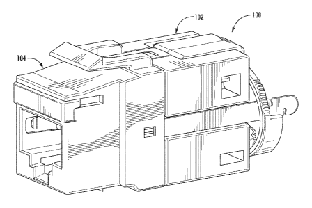
Referring initially to Figures 21 ¨ 23, the jack 100 includes a cable
termination
component 102 and receptacle component 104. The cable termination component
102
includes a front end and a rear end and is sized and configured for selective
receipt of a
plurality of conductor pairs of a cable 200 (see Figure 33). A stuffer cap
component 106,
which may be separate from or integrally formed as part of the cable
termination component
102, includes first and second lever arms 108A and 108B each having a
respective hook
element 110A and 110B, a plurality of slots 112, and opening 114 with cross
bar 116.
Each lever arm 108A and 108B includes a distal end that is free and a proximal
end
that is pivotally secured to the stuffer cap component 106, wherein the
proximal end has
the corresponding hook element 110A and 110B sized and configured for engaging
a
corresponding latch element 111A and 111B (not shown) on the receptacle
component 104.
Each lever arm 108A and 108B is selectively operable between an open position
and a
closed position, wherein force exerted by a user on the distal end either
lever arm 108A and
108B when in the open position causes the hook element 110A and 110B to engage
the
corresponding latch element 111A and 111B to secure the cable termination
component
102 to the receptacle component 104, thereby defining the closed position, as
illustrated in
Figure 21. In one embodiment, the first and second hook elements 110A and 110B
and
corresponding latch elements 111A and 111B are oppositely disposed on the
cable
termination component 102 and receptacle component 104, respectively. In
operation, use
of the lever arms 108A and 108B to secure the cable termination component 102
to the
CA 02987615 2017-11-28
WO 2016/196317 PCT/US2016/034721
receptacle component 104 completes termination without requiring the use of
secondary
tools.
Still referring to Figures 21 ¨ 23, prior to securing the cable termination
component
102 to the receptacle component 104, the wires of each of the plurality of
conductor pairs of
cable are selectively pressed into one of the plurality of slots 112 to secure
them therein.
Referring to Figures 24 ¨ 27, the receptacle component 104 includes a
plurality of
electrical contacts 14 accessible via port 122, defined by the housing of the
receptacle
component 104. The receptacle component 104 includes a full face icon 118
sized for receipt
against recessed surface 120. In one embodiment, the full face icon 118
includes clips for
attachment to corresponding sides of the recessed surface 120. The full face
icon 118 allows
for greater surface area to display information thereon. Specifically
referring to Figure 24,
opposing first segments of internal cable shield 124 are accessible via port
122. Specifically
referring to Figure 25, a plurality of offset-positioned insulation
displacement contacts (IDCs)
130 on IDC housing 132 are included, each of the plurality of offset-
positioned IDCs being
aligned for engaged abutment with a corresponding one of the wires of the
plurality of
conductor pairs when the cable termination component 102 and the receptacle
component
104 are coupled. The primary printed circuit board (PCB) 134 of the jack 100
may be housed
in the receptacle component 104, as illustrated in Figure 25.
One embodiment of the jack 100 may include an internal cable shield 124. The
internal cable shield 124 may be formed from one or more conductive materials
and
substantially surrounds the plurality of offset-positioned IDCs 130 on the
receptacle
component 104 and includes first and second protrusions 126 extending
therefrom and being
sized and configured to extend alongside opposing, outer-facing sides of the
cable
termination component 102 when the receptacle component 104 is secured to the
cable
termination component 102, wherein the first and second protrusions 126 extend
adjacently
to a portion of the cable 200. In one embodiment, the cable termination
component 102
includes recessed surfaces 127 sized for passage of the first and second
protrusions 126. Each
of the first and second protrusions 126 includes one or more notches 128, each
notch 128
being sized and configured for receipt of a cable drain wire (not pictured).
In a preferred
embodiment, the notches 128 are teardrop-shaped to facilitate securement of
the cable drain
wire thereto.
11
CA 02987615 2017-11-28
WO 2016/196317 PCT/US2016/034721
The internal cable shield 124 serves as a conductive wrap which may be
substantially
located inwards of the plastic housing of the receptacle component 104, as
there is a practical
need for part of the internal cable shield 124 to protrude from the housing in
order to, for
example, make contact with the mounted panel. As the internal cable shield 124
is primarily
located inwards of the housing, the jack 100 may effectively be color coded.
Referring to Figures 28 ¨ 30, 32 and 33, a cable ratcheting assembly on the
rear end
of the cable termination component 102 includes first and second pivoting
clamps 136A and
136B, which may each be selectively pivoted into abutment with the cable 200
in order to
relieve stress on the cable 200 at the location the cable 200 enters cable
termination
component 104. Labels 138 may be included on the cable termination component
102 for
ready identification purposes.
Referring to Figure 31, the offset placement of the IDCs 130 minimizes the
facing area
of an adjacent IDC housing 132 and jack 100 and, therefore, effectively
increases the
separation between the IDCs 130 of one jack 100 and the IDCs 130 of an
adjacent jack 100 for
improving signal transmission performance.
Referring to the foregoing description of the preferred embodiments of the
invention, it would be apparent that many modifications may be made therein.
It is to be
understood that all such modifications are embodied in the accompanying claims
which
come within the true spirit and scope of the invention.
INDUSTRIAL APPLICABILITY
The way in which the invention is capable of being exploited and the way in
which it
can be made and used will be apparent from the foregoing, particularly in
regard to
reducing electrical signal interference and return loss in electrical
connectors.
12