Note: Descriptions are shown in the official language in which they were submitted.
CA 02987686 2017-11-29
Control System and Method for Data Transmission, and Chip Array
and Display
Technical Field
The disclosure relates to the field of control, more particularly to a control
system
and method for data transmission, a chip array and a display.
Background
A Light Emitting Diode (LED) display screen is a flat display, and includes a
series of small LED module panels. Recently, due to strong applicability, rich
colour,
high light effect and long life, the LED display screen is quickly developed.
Particularly, large-screen display is a huge market of LED applications.
Currently, a data transmission mode of the LED display screen refers to that:
signals are respectively input to an input port of a first display chip in
each row of
chips in a chip array, wherein an output port of the first display chip is
connected to
an input port of a next chip; signals are transmitted sequentially according
to a series
structure sequentially formed by each row of chips, and a row of chips are
controlled
to be displayed. Aiming at the current connection mode, after a signal
transmission
speed is determined, a signal transmission range is limited within a certain
time.
When a larger signal transmission range is required, it is necessary to
increase a
signal transmission speed.
However, after the signal transmission speed is
increased, the problem of electromagnetic radiation increase will be caused,
and the
cost will be increased.
An effective solution has not proposed yet currently for the problem of
electromagnetic radiation increases when a data transmission range is
enlarged.
Summary
The embodiments of the disclosure provide a control system and method for
data transmission, a chip array and a display, which are intended to at least
solve the
technical problem in the related art that electromagnetic radiation increases
when a
data transmission range is enlarged.
According to one aspect of an embodiment of the disclosure, a control system
for data transmission is provided, which may include: a chip array, including
a
CA 02987686 2017-11-29
plurality of rows of chip assemblies, wherein any row of chip assembly
includes at
least two chip sets, all chips in each chip set are cascaded with each other;
and a
controller, configured to receive display data, and generate, according to the
display
data, a plurality of sets of display signals corresponding to the plurality of
rows of chip
assemblies, wherein any set of display signal is divided into at least two sub-
display
signals corresponding to the at least two chip sets, any sub-display signal
accesses
to a signal input end of a first chip in a corresponding chip set.
According to an example embodiment, when any row of chip assembly includes
two chip sets, a first chip set includes 211th chips in any row of chip
assembly, and a
second chip set includes 2ith chips in any row of chip assembly, i being a
natural
number.
According to an example embodiment, a signal output end of a jth chip in the
first
chip set is connected to a signal input end of a j+lth chip in the first chip
set, and a
signal output end of a jth chip in the second chip set is connected to a
signal input
end of a j+ith 19
ni in the second chip set, j being a natural number.
According to an example embodiment, when any row of chip assembly includes
three chip sets, a first chip set includes 3i-2th chips in any row of chip
assembly, a
second chip set includes 31-1 th chips in any row of chip assembly, and a
third chip set
includes 3ith chips in any row of chip assembly, i being a natural number.
According to an example embodiment, a signal output end of a jth chip in the
first
chip set is connected to a signal input end of a j+1" chip in the first chip
set, a signal
output end of a jth chip in the second chip set is connected to a signal input
end of a
j+Ith chip in the second chip set, and a signal output end of a jth chip in
the third chip
set is connected to a signal input end of a j+lth chip in the third chip set,
j being a
natural number.
According to an example embodiment, the at least two sub-display signals
formed by dividing any set of display signals are independent of each other in
transmission, signal contents of the at least two sub-display signals being
different
from each other.
According to an example embodiment, any chip in the plurality of rows of chip
assemblies corresponds to one display area.
According to an example embodiment, the display area includes a multi-row and
multi-column pixel matrix included by a plurality of pixel units.
According to another aspect of an embodiment of the disclosure, a control
2
CA 02987686 2017-11-29
method for data transmission is also provided, which may include that:
acquiring
display data; generating a plurality of sets of display signals according to
the display
data, wherein the plurality of sets of display signals correspond to a
plurality of rows
of chip assemblies in a chip array; and dividing any set of display signal
into at least
two sub-display signals, wherein any row of chip assembly includes at least
two chip
sets, the at least two sub-display signals correspond to the at least two chip
sets, and
the sub-display signal is configured to control a chip in a corresponding chip
set.
According to an example embodiment, before generating the plurality of sets of
display signals according to the display data, the method includes:
determining the
lo number of sets of the display signals according to the number of rows of
the chip
array.
According to an example embodiment, before dividing any set of display signal
into the at least two sub-display signals, the method includes: determining
the
number of the sub-display signals according to the number of sets of any row
of chip
assembly.
According to an example embodiment, when the display signal is divided into
two sub-display signals, a first sub-display signal is configured to control a
first chip
set, the first chip set including 211th chips in any row of chip assembly; and
a second
sub-display signal is configured to control a second chip set, the second chip
set
including 2ith chips in any row of chip assembly, i being a natural number.
According to an example embodiment, when the display signals are divided into
three sub-display signals, a first sub-display signal is configured to control
a first chip
set, the first chip set including 3i-2th chips in any row of chip assembly; a
second
sub-display signal is configured to control a second chip set, the second chip
set
including 3i-lth chips in any row of chip assembly; and a third sub-display
signal is
configured to control a third chip set, the third chip set including 3ith
chips in any row
of chip assembly, i being a natural number.
According to another aspect of an embodiment of the disclosure, a chip array
is
also provided, which may include a plurality of rows of chip assemblies,
wherein the
plurality of rows of chip assemblies correspond to a plurality of sets of
display signals,
and any row of chip assembly includes at least two chip sets, the at least two
chip
sets corresponding to at least two sub-display signals formed by dividing any
set of
display signal in the plurality of sets of display signals.
According to an example embodiment, a signal input end of a first chip in any
3
CA 02987686 2017-11-29
chip set is connected to a sub-display signal , and a signal output end of a
kth chip in
any chip set is connected to a signal output end of a k+1th chip in any chip
set, k
being a natural number.
According to another aspect of an embodiment of the disclosure, a display is
also provided, which may include the control system for data transmission
according
to any item in the above solution.
According to another aspect of an embodiment of the disclosure, a display is
also provided, which may include the chip array in the above solution.
In the embodiments of the disclosure, a chip array, including a plurality of
rows of
113 chip
assemblies, wherein any row of chip assembly includes at least two chip sets,
all
chips in each chip set are cascaded with each other; and a controller,
configured to
receive display data, and generate, according to the display data, a plurality
of sets of
display signals corresponding to the plurality of rows of chip assemblies,
wherein any
set of display signal is divided into at least two sub-display signals
corresponding to
the at least two chip sets, any sub-display signal accesses to a signal input
end of a
first chip in a corresponding chip set. The technical problem, in the related
art that
electromagnetic radiation increases when a data transmission range is enlarged
is
solved.
Brief Description of the Drawings
The drawings illustrated herein are used to provide further understanding of
the
disclosure, and form a part of the disclosure. The schematic embodiments and
illustrations of the disclosure are used to explain the disclosure, and do not
form
improper limits to the disclosure. In the drawings:
Fig. 1 is a schematic diagram of an example structural of the control system
for
data transmission according to the embodiment 1 of the disclosure;
Fig. 2 is a schematic diagram of an example sub-display signal transmission
where any row of chip assembly includes two chip sets according to an
embodiment
of the disclosure; and
Fig. 3 is a flowchart of an example control method for data transmission
according to the embodiment 2 of the disclosure.
Detailed Description of the Embodiments
In order to make those skilled in the art better understand the solutions of
the
4
CA 02987686 2017-11-29
disclosure, the technical solutions in the embodiments of the disclosure will
be clearly
and completely described below in conjunction with the drawings in the
embodiments
of the disclosure. Obviously, the described embodiments are only a part of the
embodiments of the disclosure, not all of the embodiments.
Based on the
embodiments of the disclosure, all other embodiments obtained on the premise
of no
creative work of those skilled in the art shall fall within the protective
scope of the
disclosure.
It is important to note that the description and claims of the disclosure and
terms
'first', 'second' and the like in the drawings are used to distinguish similar
objects, and
do not need to describe a specific sequence or a precedence order. It will be
appreciated that data used in such a way may be exchanged under appropriate
conditions, in order that the embodiments of the disclosure described here may
be
implemented in a sequence other than sequences graphically shown or described
here. In addition, terms 'include' and 'have' and any inflexions thereof are
intended
to cover non-exclusive inclusions. For instance, it is not limited for
processes,
methods, systems, products or devices containing a series of steps or units to
clearly
list those steps or units, and other steps or units which are not clearly
listed or are
inherent to these processes, methods, products or devices may be included
instead.
Embodiment 1
According to the embodiment of the disclosure, a control system for data
transmission is provided.
Fig. 1 is a schematic diagram of an example structural of the control system
for
data transmission according to the embodiment 1 of the disclosure. The system
includes:
a chip array 20, including a plurality of rows of chip assemblies, wherein any
row
of chip assembly includes at least two chip sets, all chips in each chip set
are
cascaded with each other.
According to an example embodiment, the specification of the chip array 20 may
be pre-set according to actual requirements. For instance, the specification
of the
chip array is 20*10, where 20 may represent the number of rows of the chip
array,
and 10 may represent the number of columns of the chip array. The chip array
may
include a plurality of rows of chip assemblies. For instance, the 20*10 chip
array
includes 20 rows of chip assemblies. Any row of chip assembly may include a
plurality of chip sets. For instance, each row of the 20*10 chip array
includes 10
5
CA 02987686 2017-11-29
chips; when a row of chips are divided into two chip sets, under one
situation, a first
chip set may include a first chip, a third chip, a fifth chip, a seventh chip
and a ninth
chip, and a second chip set may include a second chip, a fourth chip, a sixth
chip, an
eighth chip and a tenth chip; and under another situation, the first chip set
may
include a first chip, a second chip, a third chip, a sixth chip and a ninth
chip, and the
second chip set may include a fourth chip, a fifth chip, a seventh chip, an
eighth chip
and a tenth chip. It is important to note that which chips are included in a
chip set
may be randomly set. A signal input end of each chip in a chip set is
connected to a
signal output end in sequence. For instance, when a chip set includes a first
chip, a
to third
chip, a fifth chip, a seventh chip and a ninth chip, a signal output end of
the first
chip is connected to a signal input end of the third chip, a signal output end
of the
third chip is connected to a signal input end of the fifth chip, a signal
output end of the
fifth chip is connected to a signal input end of the seventh chip, and a
signal output
end of the seventh chip is connected to a signal input end of the ninth chip.
Here, it is also important to note that any one chip in the chip array 20 may
correspondingly control one display area. The display area may be a multi-row
and
multi-column pixel matrix included by a plurality of pixel units. For
instance, one
display area correspondingly controlled by one chip may be a 16*16 pixel
matrix.
A controller 30 is configured to receive display data and generate, according
to
the display data, a plurality of sets of display signals corresponding to the
plurality of
rows of chip assemblies, wherein any set of display signal is divided into at
least two
sub-display signals corresponding to at least two chip sets, and any sub-
display
signal access to a signal input end of a first chip in a corresponding chip
set.
According to an example embodiment, the controller 30 generates, according to
the received display data, a plurality of sets of display signals, wherein any
set of
display signal in the plurality of sets of display signals is configured to
control a row of
chip assembly corresponding to the set of display signal. Any set of display
signals
in the plurality of sets of display signals may be divided into at least two
sub-display
signals, and the number of the sub-display signals may be determined according
to
the number of chip sets in the chip assemblies. For instance, when one chip
assembly is divided into two chip sets, one set of display signal may be
divided into
two sub-display signals; and when one chip assembly is divided into three chip
sets,
one set of display signal may be divided into three sub-display signals.
In the embodiment of the disclosure, a chip array 20 includes a plurality of
rows
6
CA 02987686 2017-11-29
of chip assemblies, wherein any row of chip assembly includes at least two
chip sets,
all chips in each chip set are cascaded with each other; and a controller 30
is
configured to receive display data and generate, according to the display
data, a
plurality of sets of display signals corresponding to the plurality of rows of
chip
assemblies, wherein any set of display signal is divided into at least two sub-
display
signals corresponding to the at least two chip sets, and any sub-display
signal access
to a signal input end of a first chip in the corresponding chip set. The
technical
problem, in the related art, of electromagnetic radiation increases when a
data
transmission range is enlarged is solved.
In an optional solution of the disclosure, when any row of chip assembly
includes
two chip sets, a first chip set includes 2i-1th chips in any row of chip
assembly, and a
second chip set includes 2ith chips in any row of chip assembly, wherein i is
a natural
number.
In an optional solution of the disclosure, a signal output end of a jth chip
in a first
chip set is connected to an input end of a. th
+-1
chip in the first chip set, and a signal
output end of a jth chip in a second chip set is connected to an input end of
a j+ith
chip in the second chip set, wherein j is a natural number.
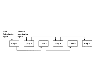
According to an example embodiment, Fig. 2 is a schematic diagram of an
example sub-display signal transmission where any row of chip assembly
includes
two chip sets according to an embodiment of the disclosure. As shown in Fig.
2, a
chip assembly including six chips is taken as an example. A first chip set
includes a
chip 1, a chip 3 and a chip 5 in a row of chip assembly, and a second chip set
includes a chip 2, a chip 4 and a chip 6 in the row of chip assembly. The
first chip
set includes three chips, wherein a first sub-display signal access to a
signal input
end of the chip 1; and the second chip set includes three chips, a second sub-
display
signal access to a signal input end of the chip 2. A signal output end of a
previous
chip in one chip set is connected to a signal input end of a subsequent chip
in the
chip set to form cascaded connection.
In an optional solution of the disclosure, it is characterized in that when
any row
of chip assembly includes three chip sets, a first chip set includes 3i-2th
chips in any
row of chip assembly, a second chip set includes 311th chips in any row of
chip
assembly, and a third chip set includes 3ith chips in any row of chip
assembly,
wherein i is a natural number.
In an optional solution of the disclosure, it is characterized in that a
signal output
7
CA 02987686 2017-11-29
end of a jth chip in a first chip set is connected to a signal input end of a
j-Fith chip in
the first chip set, a signal output end of a jth chip in a second chip set is
connected to
an input end of a j+lth chip in the second chip set, and a signal output end
of a jth chip
t
in a third chip set is connected to an input end of a j+h chip in the third
chip set,
wherein j is a natural number.
According to an example embodiment, any row of chip assembly may include
three chip sets. For instance, a first chip set includes a first chip, a
fourth chip and a
seventh chip in one row of chip assemblies, a second chip set includes a
second chip,
a fifth chip and an eighth chip in one row of chip assemblies, and a third
chip set
lo includes a third chip, a sixth chip and a ninth chip in one row of chip
assemblies.
In an optional solution of the disclosure, at least two sub-display signals
formed
by dividing any set of display signal are independent of each other in
transmission,
and signal content of the at least two sub-display signals is different from
each other.
According to an example embodiment, at least two sub-display signals formed
by dividing any set of display signal are independent of each other in
transmission.
When the problem exists in a transmission process of a sub-display signal,
other
sub-display signals are not influenced by the sub-display signal, and may be
still
normally transmitted in a chip connection mode. Signal content of the at least
two
sub-display signals is different from each other, and a sum of the signal
content forms
display data of the set of display signals.
In the embodiment of the disclosure, a chip series-parallel mixed connection
mode is adopted, signals are enabled to be transmitted in accordance with a
series-parallel mixed method, and one row of display data are controlled by
using
multiple sub-display signals. Thus, in the case of a certain transmission
speed, the
display range of the chip array 20 is multiply larger than that of series
chips, the aim
of controlling a larger range in the case of a lower transmission speed of a
signal is
achieved, and electromagnetic radiation can be effectively reduced due to the
low
transmission speed of the signal.
Embodiment 2
According to the embodiment of the disclosure, a control method for data
transmission is provided. It is important to note that the steps shown in the
flowchart
in the drawings may be executed in a computer system including a set of
computer
executable instructions, and moreover, although a logical sequence is shown in
the
flowchart, the shown or described steps may be executed in a sequence
different
8
CA 02987686 2017-11-29
from the sequence here under certain conditions.
Fig. 3 is an optional flowchart of a control method for data transmission
according to an embodiment 2 of the disclosure. As shown in Fig. 3, the method
includes the steps as follows.
Step S102: Display data is acquired.
Step S104: A plurality of sets of display signals are generated according to
the
display data, wherein the plurality of sets of display signals correspond to a
plurality
of rows of chip assemblies in a chip array.
According to an example embodiment, a controller generates, according to the
received display data, a plurality of sets of display signals, wherein any set
of display
signal in the plurality of sets of display signals is configured to control a
row of chip
assemblies corresponding to the set of display signal. The specification of
the chip
array may be pre-set according to actual requirements. The chip array may
include
a plurality of rows of chip assemblies. For instance, a 20*10 chip array may
include
20 rows of chip assemblies.
Step S106: Any display signal is divided into at least two sub-display
signals,
wherein any row of chip assembly includes at least two chip sets, the at least
two
sub-display signals correspond to the at least two chip sets, and the sub-
display
signal is configured to control a chip in a corresponding chip set.
According to an example embodiment, any set of display signal in a plurality
of
sets of display signals may be divided into at least two sub-display signals,
and the
number of the sub-display signals may be determined according to the number of
chip sets in chip assemblies. Any row of chip assembly may include a plurality
of
chip sets. For instance, each row of a 20*10 chip array includes 10 chips;
when a
row of chips are divided into two chip sets, under a situation, a first chip
set may
include a first chip, a third chip, a fifth chip, a seventh chip and a ninth
chip, and a
second chip set may include a second chip, a fourth chip, a sixth chip, an
eighth chip
and a tenth chip; and under another situation, the first chip set may include
a first
chip, a second chip, a third chip, a sixth chip and a ninth chip, and the
second chip
set may include a fourth chip, a fifth chip, a seventh chip, an eighth chip
and a tenth
chip. It is important to note that which chips are included in a chip set may
be
randomly set. A signal input end of each chip in a chip set is connected to a
signal
output end in sequence. For instance, when a chip set includes a first chip, a
third
chip, a fifth chip, a seventh chip and a ninth chip, a signal output end of
the first chip
9
CA 02987686 2017-11-29
is connected to a signal input end of the third chip, a signal output end of
the third
chip is connected to a signal input end of the fifth chip, a signal output end
of the fifth
chip is connected to a signal input end of the seventh chip, and a signal
output end of
the seventh chip is connected to a signal input end of the ninth chip. When a
chip
assembly is divided into two chip sets, a set of display signals may be
divided into
two sub-display signals; and when a chip assembly is divided into three chip
sets, a
set of display signals may be divided into three sub-display signals.
Here, it is also important to note that any chip in the chip array may
correspondingly control a display area. The display area may be a multi-row
and
multi-column pixel matrix included by a plurality of pixel units. For
instance, a
display area correspondingly controlled by a chip may be a 16*16 pixel matrix.
In Step S102, display data is acquired; in Step S104, a plurality of sets of
display
signals are generated according to the display data, wherein the plurality of
sets of
display signals correspond to a plurality of rows of chip assemblies in a chip
array;
and in Step S106, any set display signal is divided into at least two sub-
display
signals, wherein any row of chip assembly includes at least two chip sets, the
at least
two sub-display signals correspond to the at least two chip sets, and the sub-
display
signal is configured to a control chip in a corresponding chip set. The
technical
problem, in the related art, of electromagnetic radiation increases when a
data
transmission range is enlarged is solved.
In an optional solution of the disclosure, before Step S104 that the plurality
of
sets of display signals are generated according to the display data, the
method
provided by the embodiment may include that:
Step S1031: the number of sets of control signals is determined according to
the
number of rows of the chip array.
According to an example embodiment, before the controller displays a signal,
the
number of rows of chip arrays may be read first, such that the number of sets
of
generated display signals may be equal to the number of the rows of the chip
arrays.
In an optional solution of the disclosure, before Step S106 that any display
signal
is divided into at least two sub-display signals, the method provided by the
embodiment may include that:
Step S1051: the number of the sub-display signals is determined according to
the number of sets of any row of chip assembly.
According to an example embodiment, before the display signals are divided
into
CA 02987686 2017-11-29
at least two sub-display signals, the number of chip sets in any row of chip
assembly
may be read, such that the number of the generated sub-display signals may be
equal to the number of the chip sets.
In an optional solution of the disclosure, when a display signal is divided
into two
sub-display signals, the first sub-display signal is configured to control a
first chip set,
wherein the first chip set includes 2i-1th chips in any row of chip assembly;
and the
second sub-display signals may be configured to control a second chip set,
wherein
the second chip set includes 2ith chips in any row of chip assembly, i being a
natural
number.
io According to an example embodiment, as shown in Fig. 2, a chip assembly
including six chips is taken as an example. A first chip set includes a chip
1, a chip
3 and a chip 5 in one row of chip assemblies, and a second chip set includes a
chip 2,
a chip 4 and a chip 6 in one row of chip assemblies. The first chip set
includes three
chips, wherein a first sub-display signal access to a signal input end of the
chip 1;
and the second chip set includes three chips, wherein a second sub-display
signal
access to a signal input end of the chip 2. A signal output end of a previous
chip in
one chip set is connected to a signal input end of a subsequent chip in the
chip set to
form cascaded connection.
In an optional solution of the disclosure, when the display signal is divided
into
three sub-display signals, a first sub-display signal is configured to control
a first chip
set, wherein the first chip set includes 3i-2th chips in any row of chip
assembly; the
second sub-display signal is configured to control a second chip set, wherein
the
second chip set includes 3i-1th chips in any row of chip assembly; and the
third
sub-display signal is configured to control a third chip set, wherein the
third chip set
includes 31th chips in any row of chip assembly, i being a natural number.
According to an example embodiment, any row of chip assembly may include
three chip sets. For instance, a first chip set includes a first chip, a
fourth chip and a
seventh chip in one row of chip assemblies, a second chip set includes a
second chip,
a fifth chip and an eighth chip in one row of chip assemblies, and a third
chip set
includes a third chip, a sixth chip and a ninth chip in one row of chip
assemblies.
In an optional solution of the disclosure, the at least two sub-display
signals
formed by dividing the random set of display signal are independent of each
other in
transmission, and signal content of the at least two sub-display signals is
different
from each other.
11
CA 02987686 2017-11-29
In the embodiment of the disclosure, a chip series-parallel mixed connection
mode is adopted, signals are enabled to be transmitted in accordance with a
series-parallel mixed method, and one row of display data is controlled by
using
multiple sub-display signals. Thus, in the case of a certain transmission
speed, the
display range of the chip array is multiply larger than that of series chips,
the aim of
controlling a larger range in the case of a lower transmission speed of a
signal is
achieved, and electromagnetic radiation may be effectively reduced due to the
low
transmission speed of the signal.
Embodiment 3
io According to the embodiment of the disclosure, a chip array is provided.
The chip array includes a plurality of rows of chip assemblies. The plurality
of
rows of chip assemblies correspond to a plurality of sets of display signals,
and any
row of chip assembly includes at least two chip sets, wherein the at least two
chip
sets correspond to at least two sub-display signals formed by dividing any set
of
display signal in a plurality of sets of display signals, a signal input end
of a first chip
in each chip set is connected to a sub-display signal, and a signal output end
of a kth
chip in the chip sets is connected to a signal output end of a k+1th chip in
the chip
sets, k being a natural number.
According to an example embodiment, the specification of the chip array may be
pre-set according to actual requirements. For instance, the specification of
the chip
array is 20*10, where 20 may represent the number of rows of the chip array,
and 10
may represent the number of columns of the chip array. The chip array may
include
a plurality of rows of chip assemblies. For instance, the 20*10 chip array
includes
20 rows of chip assemblies Any row of chip assembly may include a plurality of
chip
sets. For instance, each row of the 20*10 chip array includes 10 chips; when a
row
of chips are divided into two chip sets, under one situation, a first chip set
may
include a first chip, a third chip, a fifth chip, a seventh chip and a ninth
chip, and a
second chip set may include a second chip, a fourth chip, a sixth chip, an
eighth chip
and a tenth chip; and under another situation, the first chip set may include
a first
chip, a second chip, a third chip, a sixth chip and a ninth chip, and the
second chip
set may include a fourth chip, a fifth chip, a seventh chip, an eighth chip
and a tenth
chip. It is important to note that which chips are included in a chip set may
be
randomly set. A signal input end of each chip in a chip set is connected to a
signal
output end in sequence. For instance, when a chip set includes a first chip, a
third
12
CA 02987686 2017-11-29
chip, a fifth chip, a seventh chip and a ninth chip, a signal output end of
the first chip
is connected to a signal input end of the third chip, a signal output end of
the third
chip is connected to a signal input end of the fifth chip, a signal output end
of the fifth
chip is connected to a signal input end of the seventh chip, and a signal
output end of
the seventh chip is connected to a signal input end of the ninth chip.
Here, it is important to note that any one chip in the chip array may
correspondingly control one display area. The display area may be a multi-row
and
multi-column pixel matrix included by a plurality of pixel units. For
instance, a
display area correspondingly controlled by a chip may be a 16*16 pixel matrix
to Here, it is also important to note that a controller generates,
according to
received display data, a plurality of sets of display signals, wherein any set
of display
signal in the plurality of sets of display signals is configured to control a
row of chip
assemblies corresponding to the set of display signal. Any set of display
signal in
the plurality of sets of display signals may be divided into at least two sub-
display
signals, and the number of the sub-display signals may be determined according
to
the number of chip sets in the chip assemblies. For instance, when one row of
chip
assembly is divided into two chip sets, one set of display signals may be
divided into
two sub-display signals; a signal output end of a kth chip in a first chip set
is
connected to a signal input end of a k+11h chip in the first chip set, and a
signal output
end of a kth chip in a second chip set is connected to an input end of a k+1th
chip in
the second chip set. When one set chip assembly is divided into three chip
sets,
one set of display signals may be divided into three sub-display signals. A
signal
output end of a kth chip in a first chip set is connected to an input end of a
k+1th chip
in the first chip set, a signal output end of a kth chip in a second chip set
is connected
to a signal input end of a k+1th chip in the second chip set, and a signal
output end of
a kth chip in a third chip set is connected to an input end of a k+1th chip in
the third
chip set.
The chip array includes a plurality of rows of chip assemblies. The plurality
of
rows of chip assemblies correspond to a plurality of sets of display signals,
and any
row of chip assembly includes at least two chip sets, wherein the at least two
chip
sets correspond to at least two sub-display signals formed by dividing any
display
signal in a plurality of sets of display signals, a signal input end of a
first chip in each
chip set is connected to a sub-display signal, and a signal output end of a
kth chip in
any chip set is connected to a signal output end of a k+1th chip in the chip
set, k
13
CA 02987686 2017-11-29
being a natural number The technical problem, in the related art, of
electromagnetic
radiation increases when a data transmission range is enlarged is solved.
Embodiment 4
According to the embodiment of the disclosure, a display is provided. The
display includes the control system for data transmission according to any
optional
solution in the embodiment 1.
Embodiment 5
According to the embodiment of the disclosure, a display is provided The
display includes the chip array according to any optional solution in the
embodiment
3.
The serial numbers of the embodiments of the disclosure are only used for
descriptions, and do not represent the preference of the embodiments.
In the above embodiments of the disclosure, descriptions of each embodiment
are emphasized respectively, and parts which are not elaborated in detail in a
certain
embodiment may refer to relevant descriptions of other embodiments.
In some embodiments provided by the disclosure, it will be appreciated that
the
disclosed technical contents may be implemented in other modes, wherein the
apparatus embodiment described above is only schematic. For instance, division
of
the units may be division of logical functions, and there may be additional
division
modes during actual implementation. For
instance, a plurality of units or
components may be combined or integrated to another system, or some features
may be omitted or may be not executed. In addition, displayed or discussed
mutual
coupling or direct coupling or communication connection may be performed via
some
interfaces, and indirect coupling or communication connection between units or
modules may be in an electrical form or other forms.
The units illustrated as separate parts may be or may not be physically
separated. Parts for unit display may be or may not be physical units. That
is, the
parts may be located at a place or may be distributed on a plurality of units.
The
aims of the solutions of the embodiments may be achieved by selecting some or
all
units according to actual requirements.
In addition, all function units in all embodiments of the disclosure may be
integrated in a processing unit, or each unit may exist separately and
physically, or
two or more units may be integrated in a unit. The integrated unit may be
14
CA 02987686 2017-11-29
implemented in a hardware form or may be implemented in a software function
unit
form.
If the integrated unit is implemented in the software function unit form and
is sold
or used as an independent product, the product may be stored in a computer
readable storage medium. Based on this understanding, the technical solutions
of
the disclosure may be substantially embodied in a software product form or
parts
contributing to the related art or all or some of the technical solutions may
be
embodied in the software product form, and a computer software product is
stored in
a storage medium, including a plurality of instructions enabling a computer
device,
which may be a personal computer, a server or a network device, to execute all
or
some of the steps of the method according to each embodiment of the
disclosure.
The storage medium includes: various media capable of storing program codes,
such
as a U disk, a Read-Only Memory (ROM), a Random Access Memory (RAM), a
mobile hard disk, a magnetic disk or an optical disc.
The control system and method for data transmission, the chip array and the
display according to the disclosure are described in an exemplar mode with
reference
to the drawings as above. However, those skilled in the art shall understand
that
various improvements may be made on the control system and method for data
transmission, the chip array and the display provided by the disclosure
without
departing from the contents of the disclosure.
The above is only preferred implementations of the disclosure. It shall be
pointed out that those skilled in the art may also make some improvements and
modifications without departing from the principle of the disclosure.
These
improvements and modifications shall fall within the protective scope of the
disclosure.