Note: Descriptions are shown in the official language in which they were submitted.
CA 02988288 2017-12-04
WO 2017/001484
PCT/EP2016/065155
DESIGN AND METHODS FOR MEASURING ANALYTES
USING NANOFABRICATED DEVICE
FIELD
[0001] This disclosure is generally related to measuring analytes, and more
specifically to sequencing linear biomolecules (e.g., DNA, RNA, proteins, and
the
like) by a nanofabricated device using quantum tunneling effects.
BACKGROUND
[0002] In genetics, the term sequencing may refer to methods for determining a
primary structure or sequence of a linear biomolecule such as DNA, RNA, amino
acids, etc. For example, DNA sequencing is the process of determining an order
of
nucleobases (adenine, guanine, cytosine and thymine) in a given DNA fragment.
DNA sequencing is a powerful method to reveal genetic variations at the
molecular
level, such as single nucleotide polymorphism, copy number variation, gene
fusion,
insertion/deletion, etc. It is thus essential to understanding disease
mechanisms,
genetic diagnosis, and personalized medicine.
[0003] DNA sequencing processes typically include extracting and fragmenting
target nucleic acids from a sample. The fragmented nucleic acids are used to
produce target nucleic acid templates that generally include one or more
adapters.
The templates can be subjected to amplification methods, such as polymerase
chain
reaction (PCR), bridge amplification to provide a cluster or rolling circle
replication in the form of a nucleic acid "nanoball," also called a DNA
nanoball
(DNB). Sequencing applications are then performed on the single-stranded
nucleic
acids, e.g., by sequencing by synthesis or by ligation techniques. Such
amplification processes, however, are generally associated with high costs,
replicative sequencing being required for high accuracy, short read lengths,
and a
long turnaround time per run (TTR).
[0004] A number of technologies for sequencing DNA at the single-molecule
level have been developed in an effort to address the disadvantages of
amplification
- 2 -
methods. For example, nanopore sequencing exploits changes in ionic current as
a
nucleobase traverses a tiny channel present in a protein or solid-state
material
subjected to an applied voltage and immersed in a conductive fluid. Further
discussion of nanopore sequencing can be found in Wang etal., The Evolution of
Nanopore Sequencing, Frontiers in Genetics, 2015, 5, 449.
Although such single-molecule sequencing
methods overcome some of the drawbacks of earlier generation amplification
methods, they nevertheless retain certain disadvantages such as low resolution
which in turn requires replicative sequencing.
100051 Very recently, devices have been demonstrated for the sequencing of
DNA using quantum tunneling current between electrodes. When a DNA segment
is present in the space between the electrodes, a change in the quantum
tunneling
current can be detected. The magnitude of change can be mapped to the
particular
nucleobase present when the measurement is made. One example of a device that
uses quantum tunneling effects to sequence DNA is a Mechanically Controllable
Break Junction (MCBJ) device. One such device is shown in FIGS. A-1B.
100061 As seen in FIG. 1A, the MCBJ device 100 includes a silicon substrate
102
on which gold electrodes 108, 108' are formed. Substrate 102 is positioned on
a
probe 104 that contacts the bottom surface of substrate 102 at a contact point
104,
and two force members 106 apply a downward force at contact points 106' of the
top surface of substrate 102. Prior to applying the force, electrodes 108,
108' are
present as a single gold electrode structure. The force creates a strain on
the
electrode structure, and is gradually increased until the electrode structure
fractures
to form electrodes 108, 108 separated by a gap 110 shown in the close-up view
at
the top-center of FIG. 1A. The force applied at contact points 106' can then
be
increased or relaxed to adjust the size of gap 110 to that required for
detecting
changes in quantum tunneling current when a DNA fragment is present in gap
110.
100071 FIG. 1B shows a Transmission Electron Microscopy (TEM) image of
MCBJ device 100 including silicon substrate 102 and a parallel array of gold
electrodes structures. The electrode structures shown in FIG. 1B have not yet
been
fractured. Upon applying the force at contact points 106' depicted in FIG. 1A,
the
CA 2988288 2019-04-15
CA 02988288 2017-12-04
WO 2017/001484
PCT/EP2016/065155
- 3 -
electrode structures of FIG. 1B will fracture to form electrodes 108, 108'
separated
by gap 110.
[0008] MCBJ device 100 shown in FIGS. 1A-1B can be used to sequence DNA
at the single-molecule level by measuring changes in quantum tunneling current
across electrodes 108, 108' when a nucleobase is present in gap 110. Device
100,
however, is associated with a number of disadvantages. For example, the
lateral
dimensions of electrodes 108, 108' must be precisely controlled in order to
create
the width of gap 110 required to observe changes in quantum tunneling current
when a nucleobase is present in gap 110. As silicon substrate 102 is flexed
after
fracture, the spacing between electrodes 108, 108' can be adjusted and thus
the
width of gap fixed at the appropriate value. None of the other electrodes in
the
array, however, may have a gap with the precise spacing required. As a result,
only
a single MCBJ sensor may function on a chip at any specific adjusted gap
width.
Further, MCBJ device 100 requires the use of gold for electrodes 108, 108'.
Due
to its high diffusivity in silicon and its tendency to form charge traps, gold
is
typically forbidden in semiconductor foundries. Thus, fabricating MCBJ device
100 requires specialized manufacturing facilities in addition to non-standard
lithography and patterning techniques.
[0009] Accordingly, it would be desirable to provide improved devices and
methods for sequencing DNA and other linear biomolecules at the single-
molecule
level.
BRIEF SUMMARY
[0010] Embodiments of the invention provide improved devices, methods of
making devices, and methods of using devices, for sequencing linear
biomolecules
at the single-molecule level using quantum tunneling effects. In some
embodiments, a nanofabricated device is provided including a substrate, a
first
electrode disposed on a first portion of a top surface of the substrate, a
dielectric
layer disposed on as second portion of the top surface of the substrate, and a
second
electrode disposed on the dielectric layer and suspended over the first
electrode. A
gap can be defined by a top surface of the first electrode and a bottom
surface of
the second electrode. The width of the gap can be nanodimensioned (e.g., 0.8
to
CA 02988288 2017-12-04
WO 2017/001484
PCT/EP2016/065155
-4-
5.0 nm) and can correspond to the size of a linear biomolecule (e.g., a DNA,
RNA,
or protein molecule) such that a quantum tunneling current is transmitted
between
the electrodes when a voltage is applied across the electrodes (i.e. when the
electrodes have different potentials) and a part of the linear molecule (e.g.,
a
nucleobase or amino acid) is present in the gap.
[0011] Other embodiments are directed to methods of making a nanofabricated
device for sequencing linear biomolecules at the single-molecule level and
using
quantum tunneling effects. The methods can incorporate deposition techniques
such as atomic layer deposition (ALD) to form the highly precise gap width
suitable for detecting changes in quantum tunneling current (or voltage) when
a
nucleobase is present in the gap. ALD can involve sequential application of
two
gas-phase precursor chemicals onto a substrate. The precursors react with the
substrate surface in a sequential, self-limiting manner. By exposing the
precursors
to the substrate surface repeatedly, a thin film can be deposited. Since the
thin film
is grown one atom or molecule at a time, the thickness of the film can be
precisely
controlled. The ALD film can be deposited between two conductive layers
patterned to form two electrodes, the spacing between the electrodes being
precisely controlled by the thickness of the ALD film. Upon removing the ALD
film from the region between the conductive layers, a gap with precise
dimensions
can be created between the electrodes. Embodiments of the invention can also
utilize other deposition techniques such as chemical vapor deposition (CVD),
physical vapor deposition (PVD), ion-beam sputtering (IBS), reactive
sputtering,
and the like to form a sacrificial film that when removed provides the gap of
desired width.
[0012] Other embodiments are directed to methods of using a nanofabricated
device for sequencing linear biomolecules at the single-molecule level and
using
quantum tunneling effects. As described above, the nanofabricated device can
include a precisely formed gap between two electrodes. Although there can be
no
direct electrical connection between the electrodes, a small amount of current
can
tunnel from one electrode to the other when a voltage is applied. Linear
biomolecules such as DNA, RNA, proteins, and the like are characterized by an
impedance. When such a linear molecule passes through the gap, the presence of
CA 02988288 2017-12-04
WO 2017/001484
PCT/EP2016/065155
- 5 -
the biomolecule can affect the amount of the quantum tunneling current.
Individual nucleobases (e.g., adenine, guanine, cytosine, and thymine) and
amino
acids are characterized by different impedance values. Thus, the change in
quantum tunneling current can depend on the particular nucleobase or amino
acid
present in the gap when the measurement is made. As the biomolecule traverses
the gap between the electrodes with the precisely defined spacing, the
sequential
changes in measured tunneling current or voltage can reflect the sequence of
the
biomolecule.
[0013] Some embodiments provide a device for sequencing a linear biomolecule
using quantum tunneling, the device comprising: a substrate having a top
surface; a
first electrode disposed on a first portion of the top surface of the
substrate; a first
dielectric layer disposed on a second portion of the top surface of the
substrate; a
second electrode disposed on the first dielectric layer and suspended over the
first
electrode; and a gap defined by a top surface of the first electrode and a
bottom
surface of the second electrode, wherein a width of the gap corresponds to a
size of
the linear biomolecule such that a quantum tunneling current is transmitted
between the first electrode and the second electrode when: a voltage is
applied
across the first electrode and the second electrode; and a part of the linear
biomolecule is present in the gap.
[0014] In some embodiments, the substrate comprises a second dielectric layer
disposed on a semiconductor substrate. In further embodiments, the width of
the
gap is about 0.8 to 5.0 nm. In some embodiments, the gap is further defined by
a
top surface of the first dielectric layer and a side surface of the second
electrode. In
further embodiments, the top surface of the first dielectric layer and the top
surface
of the first electrode are substantially coplanar. In some embodiments, the
first
electrode and the second electrode are oriented orthogonally to one another.
In
further embodiments, the device further comprises circuitry electrically
coupled to
the first electrode and the second electrode, wherein the circuitry is
configured to:
apply the voltage across the first electrode and the second electrode; and
measure:
the quantum tunneling current transmitted between the first electrode and the
second electrode; the voltage across the first electrode and the second
electrode; or
an impedance between the first electrode and the second electrode. In some
CA 02988288 2017-12-04
WO 2017/001484
PCT/EP2016/065155
- 6 -
embodiments, the first electrode and the second electrode individually
comprise a
material selected from a group consisting of metals, semiconductors, carbon,
conductive ceramics, and conductive polymers. In further embodiments, the
first
dielectric layer comprises a material selected from the group consisting of
oxides,
dielectric ceramics, polymers, carbonates, glasses, minerals, and air.
[0015] Other embodiments provide a method of making a device for sequencing
a linear biomolecule using quantum tunneling, the method comprising: providing
a
substrate having a top surface; depositing a first electrode onto a first
portion of the
top surface of the substrate; depositing a first dielectric layer onto a
second portion
of the top surface of the substrate; depositing a sacrificial layer onto a top
surface
of the first electrode; depositing a second electrode onto the sacrificial
layer and
onto a top surface of the first dielectric layer; and removing the sacrificial
layer,
thereby forming a gap defined by the top surface of the first electrode and a
bottom
surface of the second electrode, wherein a width of the gap corresponds to a
size of
the linear biomolecule such that a quantum tunneling current is transmitted
between the first electrode and the second electrode when: a voltage is
applied
across the first electrode and the second electrode; and a part of the linear
biomolecule is present in the gap.
[0016] In some embodiments, the substrate comprises a second dielectric layer
disposed on a semiconductor substrate. In further embodiments, the width of
the
gap is about 0.8 to 5.0 nm. In some embodiments, the sacrificial layer is
further
deposited onto the top surface of the first dielectric layer, wherein the gap
is further
defined by the top surface of the first dielectric layer and a side surface of
the
second electrode. In further embodiments, the top surface of the first
dielectric
layer and the top surface of the first electrode are substantially coplanar.
In some
embodiments, the first electrode and the second electrode are oriented
orthogonally
to one another. In further embodiments, the sacrificial layer is deposited
using an
atomic layer deposition process. In some embodiments, the sacrificial layer is
removed using an etching process, wherein the etching process includes
exposing
the sacrificial layer to an etchant. In further embodiments, the sacrificial
layer
comprises a material selected from the group consisting of metals, oxides,
nitrides,
and carbon containing materials. In some embodiments, the etchant comprises a
CA 02988288 2017-12-04
WO 2017/001484
PCT/EP2016/065155
- 7 -
substance selected from the group consisting of hydrofluoric acid, phosphoric
acid,
hydrochloric acid, nitric acid, sodium hydroxide, SC-1 solution, organic
solvents,
and 02 plasma. In further embodiments, the method further comprises
electrically
coupling circuitry to the first electrode and the second electrode, wherein
the
circuitry is configured to: apply the voltage across the first electrode and
the second
electrode; and measure: the quantum tunneling current transmitted between the
first
electrode and the second electrode; the voltage across the first electrode and
the
second electrode; or an impedance between the first electrode and the second
electrode. In some embodiments, the first electrode and the second electrode
individually comprise a material selected from the group consisting of metals,
semiconductors, carbon, conductive ceramics, and conductive polymers. In
further
embodiments, the first dielectric layer comprises a material selected from the
group
consisting of oxides, dielectric ceramics, polymers, carbonates, glasses,
minerals,
and air.
[0017] Other embodiments provide a method of using a device for sequencing a
linear biomolecule using quantum tunneling, the method comprising: providing
the
device comprising: a substrate having a top surface; a first electrode
disposed on a
first portion of the top surface of the substrate; a first dielectric layer
disposed on a
second portion of the top surface of the substrate; a second electrode
disposed on
the first dielectric layer and suspended over the first electrode; a gap
defined by a
top surface of the first electrode and a bottom surface of the second
electrode; and
circuitry electrically coupled to the first electrode and the second
electrode;
applying, using the circuitry, a voltage across the first electrode and the
second
electrode; introducing a part of the linear biomolecule into the gap;
measuring,
using the circuitry: a quantum tunneling current transmitted between the first
electrode and the second electrode; the voltage across the first electrode and
the
second electrode; or an impedance between the first electrode and the second
electrode; and identifying, based on the measured quantum tunneling current,
the
measured voltage, or the measured impedance, the part of the linear
biomolecule
introduced into the gap.
[0018] In some embodiments, the linear biomolecule is selected from the group
consisting of DNA, RNA, polypeptides, and proteins. In further embodiments,
the
CA 02988288 2017-12-04
WO 2017/001484
PCT/EP2016/065155
- 8 -
part of the linear biomolecule comprises a nucleobase or an amino acid. In
some
embodiments, the substrate comprises a second dielectric layer disposed on a
semiconductor substrate. In further embodiments, a width of the gap is about
0.8 to
5.0 nm. In some embodiments, the gap is further defined by a top surface of
the
first dielectric layer and a side surface of the second electrode, wherein the
top
surface of the first dielectric layer and the top surface of the first
electrode are
substantially coplanar, and wherein the first electrode and the second
electrode are
oriented orthogonally to one another. In further embodiments, the first
electrode
and the second electrode individually comprise a material selected from the
group
consisting of metals, semiconductors, carbon, conductive ceramics, and
conductive
polymers. In some embodiments, the first dielectric layer comprises a material
selected from the group consisting of oxides, dielectric ceramics, polymers,
carbonates, glasses, minerals, and air.
[0019] A better understanding of the nature and advantages of embodiments of
the present invention may be gained with reference to the following detailed
description and the accompanying drawings.
BRIEF DESCRIPTION OF THE DRAWINGS
[0020] FIG IA shows a schematic of an existing MCBJ device used to sequence
DNA by measuring quantum tunneling current across a break junction formed
between gold electrodes.
[0021] FIG. 1B shows a TEM image of the MCBJ depicted in FIG. 1A including
the gold electrode structure prior to forming the break junction.
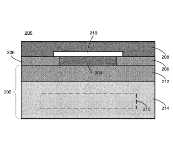
[0022] FIG. 2A shows a schematic cross-sectional side view of a nanofabricated
device for sequencing linear biomolecules using quantum tunneling according to
embodiments of the present invention.
[0023] FIG. 2B shows a schematic top view of a nanofabricated device for
sequencing linear biomolecules using quantum tunneling according to
embodiments of the present invention.
CA 02988288 2017-12-04
WO 2017/001484
PCT/EP2016/065155
- 9 -
[0024] FIGS. 3A-3H illustrate a method of making a device for sequencing a
linear biomolecule using quantum tunneling according to embodiments of the
present invention.
[0025] FIG. 4 shows a flowchart illustrating a method of using a device for
sequencing a linear biomolecule using quantum tunneling according to
embodiments of the present invention.
[0026] FIG. 5 shows a block diagram of an exemplary computer system usable to
sequence linear biomolecules using quantum tunneling according to embodiments
of the present invention.
DEFINITIONS
[0027] The following definitions may be helpful in providing background for an
understanding of embodiments of the invention.
[0028] A "linear biomolecule" refers to a type of molecule that is present in
a
living organism in the form of polymers containing monomeric units that are
covalently bonded to form larger chain-like structure. Exemplary linear
biomolecules include, but are not limited to, polynucleotides (e.g., DNA and
RNA), polypeptidcs, and proteins. In some embodiments, linear biomolccules can
also include branched or cyclic biomolecules including one or more linear
portions.
[0029] A "part of a linear molecule" refers to a monomer of a linear
biomolecule.
Exemplary parts of linear biomolecules include, but are not limited to,
nucleobases
and amino acids.
[0030] A "nucleobase" refers to nitrogen-containing organic molecules that
serve
as the monomers of polynucleotides such as DNA and RNA. Exemplary
nucleobases include, but are not limited to, cytosine, guanine, adenine,
thymine,
and uracil.
[0031] An "amino acid" refers to organic compounds comprising amine and
carboxylic acid groups, and a side-chain, and that serve as the monomers of
polypeptides and proteins.
CA 02988288 2017-12-04
WO 2017/001484
PCT/EP2016/065155
- 10 -
[0032] "Quantum tunneling" refers to the quantum mechanical phenomenon
where a particle tunnels through an energy barrier that classical (i.e.
Newtonian)
mechanics conclude could not be overcome by the particle. In the case of
electrons
tunneling through an energy barrier between two electrodes, such tunneling is
referred to as "quantum tunneling current."
[0033] An "electrode" refers to a circuit element comprising an electrically
conducting material and that makes contact with a nonmetallic part of a
circuit such
as air or vacuum. Suitable electrically conductive materials include, but are
not
limited to, metals, semiconductors, carbon, conductive ceramics, and
conductive
polymers.
[0034] A "dielectric layer" refers to a layer comprising an insulator material
that
is a poor electrical conductor. Exemplary dielectric materials include, but
are not
limited to, oxides, dielectric ceramics, polymers, carbonates, glasses,
mineral, and
air.
[0035] "Atomic layer deposition" refers to a thin film deposition technique
where one or more precursors in the gas phase react with the surface of a
substrate
in a self-limiting manner such that the reaction terminates once all reactive
sites on
the surface are consumed. In some embodiments, atomic layer deposition can
involve exposing a substrate to two gas phase precursors in a sequential
manner. In
some other embodiments, atomic layer deposition can involve depositing a thin
film by way of a single precursor using, for example, plasma or radical
enhanced
processes.
[0036] A "sacrificial layer" refers to a formed layer of material that is
subsequently removed by a process such as etching. Exemplary sacrificial layer
materials include, but are not limited to, metals, oxides, nitrides, and
carbon
containing materials.
[0037] "Etching" refers to the process of using a corrosive substance (i.e. an
etchant) to dissolve a solid material. Exemplary etchants include, but are not
limited to, hydrofluoric acid, phosphoric acid, hydrochloric acid, nitric
acid,
sodium hydroxide, SC-1 solution, organic solvents, and etching by plasmas.
CA 02988288 2017-12-04
WO 2017/001484
PCT/EP2016/065155
- 11 -
Plasma etching can involve a stream of glow discharge (plasma) of an
appropriate
gas mixture. The plasma source, known as etch species, can be either charged
(ions) or neutral (atoms and radicals) created in a vacuum system by way of
radio
frequency or microwave excitations. "Selective etching" refers to the process
of
selecting and using a particular etchant that dissolves a first solid material
but does
not dissolve a second solid material that may be adjacent to the first solid
material.
[0038] "Circuitry" refers to an electronic circuit or system of electronic
circuits
that perform one or more functions in an electronic device. Electronic
circuits can
include electronic components such as resistors, transistors, capacitors,
inductors,
and diodes, connected by conductive wires or traces through which electrical
current can flow. Circuitry can include one or more integrated circuits and,
in
some embodiments, can include software executed by one or more integrated
circuits.
DETAILED DESCRIPTION
[0039] Embodiments can provide improved devices, methods of making devices,
and methods of using devices, for sequencing linear biomolecules at the single-
molecule level using quantum tunneling effects. In some embodiments, a
nanofabricated device is provided including a precisely formed gap disposed
between two electrodes and having a very small width (e.g., 0.8 to 5.0 nm).
The
width of the gap can correspond to the size of a linear biomolecule such as
DNA,
RNA, a polypeptide, a protein, and the like. When a part of the linear
biomolecule
(e.g., a nucleobase or amino acid) is present in the gap and a voltage is
applied
across the electrodes, a change in quantum tunneling current (or voltage) can
be
measured. The magnitude of the change can be mapped to the particular
biomolecule part present at the time of measurement. As the linear biomolecule
(or
molecular fragment) traverses the gap, sequencing can be performed by taking
subsequent measurements at time intervals selected based upon the
biomolecule's
traversal velocity.
[0040] The precisely dimensioned gap can be formed by depositing a thin film
between two electrodes using a deposition process such as ALD. The sacrificial
film can then be removed by way of selective etching, with the resulting void
CA 02988288 2017-12-04
WO 2017/001484
PCT/EP2016/065155
- 12 -
forming the gap. Since processes such as ALD can deposit layers of a desired
material having the thickness of a single atom or molecule, film thickness can
be
accurately controlled, thereby resulting in a quantum tunneling gap engineered
to
having the desired width at a very high level of precision. Moreover, by using
deposition processes to form the nanofabricated devices of the present
invention,
many detectors can be placed on a single integrated circuit chip. Due to the
large
number of nucleobases in a DNA or RNA molecule, for example, sequencing can
be performed at a rapid pace as many fragments can be sequenced
simultaneously.
[0041] Further, methods of the present invention for making nanofabricated
devices can be performed using generally available semiconductor processing
equipment and using materials commonly used in semiconductor foundries. Some
semiconductor foundries forbid the use of gold and certain other transitional
metals
that can act as charge recombination centers. Such metals show high
diffusivity in
silicon, and thus contamination on a wafer surface can lead to charge traps
being
formed in depletion regions of the p-n junctions during thermal processing.
Although embodiments of the present invention can utilize gold as an electrode
material (i.e. as done in existing MCBJ devices), materials other than gold
and
charge trap-forming transition metals can be used. In some embodiments,
methods
of the present invention can also use existing semiconductor fabrication
techniques
(e.g., deposition, photolithography, etching, and the like) to form the
nanofabricated devices. By using processing equipment, techniques, and
materials
compatible with existing semiconductor fabrication, the nanofabricated devices
of
the present invention can be made in a more time efficient and cost-effective
manner as compared to existing single-molecule sequencing devices.
I. NANOFABRICATED DEVICE
[0042] FIGS. 2A-2B show schematics of a nanofabricated device 200 for
sequencing linear biomolecules using quantum tunneling according to
embodiments of the present invention. FIG. 2A shows a cross-sectional side
view
of device 200, and FIG. 2B shows a top view of device 200. It should be noted
that
the schematics of device 200 shown in FIGS. 2A-2B are merely one possible
CA 02988288 2017-12-04
WO 2017/001484
PCT/EP2016/065155
- 13 -
configuration, and that one of skill in the art will appreciate that
embodiments of
the present invention encompass other configurations.
[0043] As shown in FIG. 2A, device 200 can include a substrate 202 having a
top
surface, a first electrode 204 disposed on a first portion of the top surface
of
substrate 202, a first dielectric layer 206 disposed on a second portion of
the top
surface of substrate 202, and a second electrode 208 disposed on first
dielectric
layer 206 and suspended over first electrode 204. As shown in FIG. 2A, device
200 can include a gap 210 defined by a top surface of first electrode 204 and
a
bottom surface of second electrode 208. The width of gap 210 (i.e. the
distance
between the top surface of first electrode 204 and the bottom surface of
second
electrode 208) can correspond to a size of a linear biomolecule such that a
quantum
tunneling current is transmitted between first electrode 204 and second
electrode
208 when a voltage is applied across first electrode 204 and second electrode
208
and a part of the linear biomolecule is present in gap 210.
[0044] As described in further detail below, the width of gap 210 can be
precisely dimensioned using a deposition process such as ALD to form a
sacrificial
layer between first electrode 204 and second electrode 208. The sacrificial
layer
can be subsequently removed (e.g., via selective etching) to form gap 210. The
width of gap 210 can be dimensioned to correspond to the size of the type of
linear
biomolecule to be sequenced using device 200. In some embodiments, the width
of
gap 210 can be about 0.8 to 5.0 nm. When device 200 is used to sequence small
linear biomolecules such as DNA or RNA, the width of gap 210 can be about 0.8
to
1.2 nm in some embodiments. For larger biomolecules such as polypeptides or
proteins, the width of gap 210 can be about 1.2 to 5.0 nm in some embodiments.
[0045] The width of gap 210 can be adjustable in some embodiments. For
example, first dielectric layer 206 can include (or be replaced by) a
piezoelectric
element comprising a material that expands in volume in response to an applied
electromagnetic field. As shown in FIG. 2A, in this non-limiting example, an
expansion of the piezoelectric element in the vertical direction can cause
second
electrode 208 to move in the vertical direction, thereby increasing the width
of gap
210.
CA 02988288 2017-12-04
WO 2017/001484
PCT/EP2016/065155
- 14 -
[0046] In some embodiments, as shown in FIG. 2A, gap 210 can be further
defined by a top surface of first dielectric layer 206 and a side surface of
second
electrode 208. In such embodiments, the top surface of first dielectric layer
206
and the top surface of first electrode 204 can be substantially coplanar. In
some
other embodiments, first electrode 204 can be recessed such that its top
surface is
in a plane below that formed by the top surface of first dielectric layer 206.
In such
embodiments, gap 210 can be further defined by a side surface of first
dielectric
layer 206.
[0047] First electrode 204 and second electrode 208 can each comprise any
suitable electrically conductive material, including but not limited to,
metals,
semiconductors, carbon, conductive ceramics, and conductive polymers.
Exemplary metals can include Cu, W, Ti, Au, Ag, Al, Zn, Ni, Fe, Pt, Ta, and
the
like. Exemplary semiconductors can include Si, Ge, SiGe, GaAs, InP, and the
like.
Exemplary carbon allotropes and morphologies can include diamond, graphite,
graphene, nanotubes, nanofibers, vapor grown carbon fiber (VGCF), and the
like.
In some embodiments, carbon-containing compounds can be used as the material
for first electrode 204 and second electrode 208. Exemplary conductive
ceramics
can include TiN, TaN, indium tin oxide (ITO), lanthanum-doped strontium
titanate
(SLT), yttrium-doped strontium titanate (SYT), and the like. Exemplary
conductive polymers can include poly(pyrrole)s (PPY), polyanilines (PANI),
poly(thiophenc)s (PT), poly(3,4-cthylenedioxythiophene) (PEDOT), poly(p-phenyl
sulfide) (PPS), poly(acetylene)s (PAC), poly(p-phenylene vinylene) (PPV), and
the
like.
[0048] In some embodiments, first electrode 204 and second electrode 208 can
comprise the same electrically conductive material. In other embodiments,
first
electrode 204 and second electrode 208 can comprise different electrically
conductive materials.
[0049] First dielectric layer 206 can comprise any suitable electrically
insulating
material including, but not limited to, oxides, dielectric ceramics, polymers,
carbonates, glasses, minerals, and air. Exemplary oxides can include SiO2,
Sl205,
A1203, ZrO2, Fe203, MgO, ZnO, Ta205, Hf02, titanates, and the like. Exemplary
CA 02988288 2017-12-04
WO 2017/001484
PCT/EP2016/065155
- 15 -
dielectric ceramics can include Si3N4, SiC, SiAlON, MN, and the like.
Exemplary
polymers can include paralene, photopolymers (e.g., photoresists), hydrocarbon
rubbers (e.g., EPM, EPDM, and the like), nitriles, polyethylenes,
polyurethanes,
silicones, and the like. Exemplary carbonates can include CaCO3, MgCO3, and
the
like. Exemplary glasses can include borosilicate glass, soda-lime glass, and
the
like. Exemplary minerals can include mica, steatite, cordierite, and the like.
[0050] As shown in FIG. 2A, in some embodiments, substrate 202 can include a
second dielectric layer 212 disposed on a semiconductor substrate 214. Second
dielectric layer 212 can comprise any suitable electrically insulating
material
described above with respect to first dielectric layer 206. In some
embodiments,
first dielectric layer 206 and second dielectric layer 212 can comprise the
same
electrically insulating material. In other embodiments, first dielectric layer
206 and
second dielectric layer 212 can comprise different electrically insulating
materials.
In FIG. 2A, first dielectric layer 206 and second dielectric layer 212 are
depicted as
two separate layers. In some embodiments, first dielectric layer 206 and
second
dielectric layer 212 in combination can be a single layer of electrically
insulating
material.
[0051] Semiconductor substrate 214 can comprise any suitable semiconducting
material including, but not limited to, Si, Ge, SiGe, GaAs, InP, and the like.
In
some embodiments, semiconductor substrate 214 can be an integrated circuit
chip
comprising circuitry 216 which can be electrically coupled to first electrode
204
and second electrode 208. For example, in some embodiments, circuitry 216 can
be electrically coupled to first electrode 204 using a first via through
second
dielectric layer 212, and circuitry 216 can be electrically coupled to second
electrode 208 using a second via through second dielectric layer 212 and first
dielectric layer 206. Circuitry 216 can be configured to apply a voltage
across first
electrode 204 and second electrode 208, and measure quantum tunneling current
transmitted between (or the voltage across) first electrode 204 and second
electrode
208.
[0052] As described herein, when a part of a linear biomolecule is present in
gap
210 and a voltage is applied across first electrode 204 and second electrode
208, a
CA 02988288 2017-12-04
WO 2017/001484
PCT/EP2016/065155
- 16 -
quantum tunneling current can be transmitted between first electrode 204 and
second electrode 208. The measured quantum tunneling current (or resulting
voltage) can be mapped to the particular part of the biomolecule present in
gap 210,
and sequencing can be accomplished by repeating the measurements as the
biomolecule traverses gap 210. Circuitry 216 can be configured to perform such
mapping operations or, alternatively, can transmit current or voltage
measurements
to an external computing device configured to perform some or all of the
mapping
operations.
[0053] In FIG. 2A, circuitry 216 is depicted as being contained within
semiconductor substrate 214 of device 200. In other embodiments, all or a
portion
of circuitry 216 can be present outside substrate 202. For example, one or
more
transistors, capacitors, resistors, diodes, and/or inductors of circuitry 216
can reside
external to substrate 202 or external to device 200 altogether. For example,
in
some embodiments, all or a portion of circuitry 216 can be in the form of an
external integrated circuit chip or in any other suitable configuration
external to
device 200.
[0054] FIG. 2B shows a schematic top view of device 200 including first
electrode 204, first dielectric layer 206, and second electrode 208. As
depicted in
FIG. 2B, first electrode 204 and second electrode 208 can be oriented
orthogonally
to one another. This, however, is not intended to be limiting. In other
embodiments, first electrode 204 and second electrode 208 can be oriented
parallel
to one another or at any suitable angle between 0 and 180 so long as gap 210
is
present between first electrode 204 and second electrode 208.
[0055] Device 200 can be one of many devices on a single integrated circuit
chip.
For example, the top surface of semiconductor substrate 214 can be large
enough to
support an array of many devices each including first dielectric layer 206,
second
dielectric layer 212, first electrode 204, second electrode 208, and gap 210.
In
some embodiments, each device can be separated by a dielectric layer to
prevent
electrodes in adjacent devices from coming into electrical or physical contact
with
one another. In some embodiments, each device in an array can include its own
circuitry (e.g., circuitry 216) for applying voltages and measuring quantum
CA 02988288 2017-12-04
WO 2017/001484
PCT/EP2016/065155
- 17 -
tunneling current or voltage generated within the specific device (i.e. device
200).
In some other embodiments, the circuitry for multiple devices can be
integrated
such that circuitry 216 applies voltages and measures quantum tunneling
currents
or voltages when linear biomolecules are present in the gaps of some or all of
the
devices in the array.
[0056] By providing multiple devices on a single integrated circuit chip, many
biomolecule fragments can be sequenced simultaneously since quantum tunneling
current and voltage measurements can be made as the fragments traverse the
gaps
of each device in the array. As a result, linear biomolecules can be sequenced
at
the single-molecule level with improved speed and efficiency.
METHOD OF MAKING NANOFABRICATED DEVICE
[0057] Embodiments of the invention also provide methods of making a
nanofabricated device for sequencing linear biomolecules at the single-
molecule
level and using quantum tunneling effects. In such methods, generally
available
semiconductor processing equipment and materials compatible with existing
semiconductor fabrication processes can be used. Moreover, existing
semiconductor fabrication techniques (e.g., photolithography, etching,
deposition,
and the like) can be used to form the nanofabricated devices. As a result, the
nanofabricated devices of the present invention can be made in a more time
efficient and cost-effective manner as compared to existing single-molecule
sequencing devices.
A. Semiconductor Manufacturing Processes
[0058] Embodiments of the invention provide methods of making nanofabricated
devices using, at least in part, existing semiconductor fabrication techniques
such
as photolithography, electron-beam (e-beam) lithography, etching, deposition,
and
the like.
[0059] Photolithography is used in the semiconductor industry to pattern solid
materials such as semiconductor (e.g., Si) wafers. The technique uses light to
transfer a geometric pattern from a photomask to a light-sensitive chemical
called a
"photoresist" disposed on the material surface. The photomask can be an opaque
CA 02988288 2017-12-04
WO 2017/001484
PCT/EP2016/065155
- 18 -
plate including transparent regions that allow light to shine through in the
particular
geometric pattern. Subsequent chemical treatments can be used to engrave the
exposure pattern into the material underneath the photoresist, and such
treatments
can also be used to allow a new material to be deposited in the geometric
pattern.
Several photolithography cycles can be performed to fabricate a material
having
the desired microstructure, with each iteration involving several steps
performed
sequentially.
[0060] In an exemplary photolithography process, the starting material is
initially
cleaned using a wet chemical treatment (e.g., hydrogen peroxide,
trichloroethylene,
acetone, methanol, or the like) to remove surface contaminants. The material
is
then heated to evaporate any moisture on the surface, and a chemical such as
bis(trimethylsilyl)amine is applied to promote adhesion of the photoresist to
the
material surface. Using a spin coating process, a liquid photoresist solution
is then
applied to the material to form a coating having a uniform thickness of, for
example, about 3 microns or less. Exemplary photoresists can include, but are
not
limited to, poly(methyl methacrylate) (PMMA), poly(methyl glutarimide) (PMGI),
phenol formaldehyde resin, SU-8, and the like. The coated material is then
prebaked to evaporate any excess photoresist solution.
[0061] The photoresist coated material is subjected to a pattern of intense UV
or
X-ray light which causes a chemical change in the photoresist layer that
allows the
photoresist material to be removed using a developer solution such as
tetramethylammonium hydroxide (TMAH). If a "positive" photoresist is used, the
regions exposed to the UV (or X-ray) light can dissolve in the developer
solution.
Alternatively, in the case of a "negative photoresist," the non-exposed
regions of
the photoresist can dissolve in the developer solution. After a post-exposure
bake
(PEB), the developer solution is applied followed by a "hard-baking" to
solidify the
photoresist pattern remaining on the surface of the material.
[0062] An etching process can then be used to remove the regions of material
not
coated with the photoresist, thereby forming the desired geometric pattern in
the
material. This can be accomplished using a liquid etchant (e.g., hydrofluoric
acid,
phosphoric acid, hydrochloric acid, nitric acid, sodium hydroxide, SC-1
solution,
CA 02988288 2017-12-04
WO 2017/001484
PCT/EP2016/065155
- 19 -
organic solvents, and the like) or a plasma etchant (e.g., oxygen, argon, and
the
like). The photoresist can then be removed using a liquid resist stripper such
as 1-
Methy1-2-pyrrolidon (NMP) or a plasma (e.g., containing oxygen).
[0063] Other techniques such as e-beam lithography are also used in the
semiconductor industry to pattern solid materials. E-beam lithography is a
process
very similar to photolithography as described above, except that e-beam
lithography uses a beam of electrons (instead of light) to transfer a
geometric
pattern by selectively modifying the solubility of an electron-sensitive
resist layer
disposed on the material surface. E-beam lithography can be used to transfer
geometric patterns at a very small scale (e.g., 10 nm or less).
[0064] The photolithography and e-beam lithography techniques described above
can be used in some embodiments of the invention to remove regions of material
during fabrication of a nanofabricated device for sequencing linear
biomolecules.
In some embodiments, deposition techniques used in the semiconductor industry
can be used to add regions of material when forming the nanofabricated devices
described herein. For example, deposition techniques can be used to deposit
material into a cavity or void formed by regions of material being removed
during
photolithography followed by etching processes. Such deposition techniques can
include, but are not limited to, atomic layer deposition (ALD), chemical vapor
deposition (CVD), physical vapor deposition (PVD), ion-beam sputtering (IBS),
and reactive sputtering.
[0065] ALD involves deposition of a thin film by causing one or more
precursors
to react with the surface of a substrate in a self-limiting manner, the
resulting film
being grown one atomic (or molecular) layer at a time with each iteration. CVD
refers to a process where a substrate is exposed to one or more volatile
precursors
which react or decompose on the substrate surface, thereby forming a deposited
layer of material. Any volatile byproducts can be transported out of the CVD
reaction vessel using a gas flow. In PVD, a thin film is deposited onto a
substrate
by condensing the target film material from its vapor phase. IBS involves
generating ions of a source material by colliding the material with electrons
confined by a magnetic field in a vacuum chamber. An electric field
accelerates
CA 02988288 2017-12-04
WO 2017/001484
PCT/EP2016/065155
- 20 -
the ions towards a substrate, with the ions being neutralized by electrons
from an
external filament prior to striking the substrate and forming the layer of
desired
material. Reactive sputtering is similar to IBS, with a difference being that
a
reactive gas (e.g., oxygen, nitrogen, CO2, C2H2, or CH4) is introduced into
the
vacuum chamber, the gas reacting with the source material ions to form layers
on
the substrate comprising, for example, oxides, nitrides, metal-DLCs, carbides,
or
carbo-nitrides.
B. Method of Making a Nanofabricated Device
[0066] FIGS. 3A-3H illustrate a method of making a nanofabricated device for
sequencing a linear biomolecule using quantum tunneling according to
embodiments of the present invention. The method can utilize photolithography,
etching, and deposition techniques used in existing semiconductor fabrication
processes to form a layered device including two electrodes separated by a
gap.
The gap can have a width that corresponds to the size of a linear biomolecule
(e.g.,
DNA, RNA, polypeptide, protein, or the like) to be sequenced, such that a
quantum
tunneling current is transmitted between the electrodes when a part (e.g., a
nucleobase or amino acid) is present in the gap. It should be noted that the
method
and resulting device depicted in FIGS. 3A-3H are merely one example, and that
one of skill in the art will appreciate that embodiments of the present
invention
encompass modifications to the described method leading to structural
modifications to the resulting device.
[0067] As shown in FIG. 3A, the method can begin by providing a substrate 302
having a top surface onto which a first dielectric layer 306 can be deposited
as
shown in FIG. 3B. First dielectric layer 306 can be deposited using any
suitable
deposition technique described herein.
[0068] First dielectric layer 306 can comprise any suitable electrically
insulating
material including, but not limited to, oxides, dielectric ceramics, polymers,
carbonates, glasses, minerals, and air. Exemplary oxides can include 5i02,
5i203,
A1203, ZrO2, Fe2O3, MgO, ZnO, Ta205, Hf02, titanates, and the like. Exemplary
dielectric ceramics can include Si3N4, SiC, SiAlON, AIN, and the like.
Exemplary
polymers can include hydrocarbon rubbers (e.g., EPM, EPDM, and the like),
CA 02988288 2017-12-04
WO 2017/001484
PCT/EP2016/065155
-21 -
nitriles, polyethylenes, polyurethanes, silicones, and the like. Exemplary
carbonates an include CaCO3, MgCO3, and the like. Exemplary glasses can
include soda-lime glass and the like. Exemplary minerals can include mica,
steatite, cordierite, and the like.
[0069] In some embodiments, as shown in FIGS. 3A-3B, substrate 302 can
include a second dielectric layer 312 disposed on a semiconductor substrate
314.
Second dielectric layer 312 can comprise any suitable electrically insulating
material described above with respect to first dielectric layer 306. In some
embodiments, first dielectric layer 306 and second dielectric layer 312 can
comprise the same electrically insulating material. In other embodiments,
first
dielectric layer 306 and second dielectric layer 312 can comprise different
electrically insulating materials.
[0070] In FIGS. 3A-3B, first dielectric layer 306 and second dielectric layer
312
are depicted as two separate layers. In such embodiments, substrate 302 can be
formed by depositing second dielectric layer 312 onto semiconductor substrate
314
using any suitable deposition technique described herein, with the top surface
of
substrate 302 being the top surface of second dielectric layer 312. In some
other
embodiments, first dielectric layer 306 and second dielectric layer 312 in
combination can be a single layer of electrically insulating material. For
example,
a single dielectric layer having the combined thickness of first dielectric
layer 306
and second dielectric layer 312 shown in FIGS. 3A-3B can be deposited onto the
top surface of semiconductor substrate 314.
[0071] Semiconductor substrate 314 can comprise any suitable semiconducting
material including, but not limited to, Si, Ge, SiGe, GaAs, InP, and the like.
In
some embodiments, semiconductor substrate 314 can be an integrated circuit
chip
comprising circuitry 316 which can be formed within semiconductor substrate
314
before, after, or during fabrication of the nano fabricated device according
to
various embodiments of the invention.
[0072] In FIG. 3C, a cavity 306' can be formed by removing a region of first
dielectric layer 306. In some embodiments, cavity 306' can be formed using a
photolithography process where a photoresist layer is applied to the top
surface
CA 02988288 2017-12-04
WO 2017/001484
PCT/EP2016/065155
- 22 -
first dielectric layer 306 shown in FIG. 3B. The photoresist coated surface
can then
be exposed to UV light in the desired geometric pattern such that a region of
the
photoresist is dissolved when placed in contact with a developer solution. An
etchant can then be used to selectively etch away the region of first
dielectric layer
306 to form cavity 306' while preserving the adjacent regions of first
dielectric
layer 306 protected by the photoresist.
[0073] As shown in FIG. 3D, a first electrode 304 can be deposited onto the
top
surface of substrate 302 and in cavity 306' formed in first dielectric layer
306. First
electrode 304 can be deposited using any suitable deposition technique
described
herein. The resulting structure, as shown in FIG. 3D, can include first
electrode
304 being disposed on a first portion of the top surface of substrate 302, and
first
dielectric layer 306 being disposed on a second portion of the top surface of
substrate 302.
[0074] First electrode 304 can comprise any suitable electrically conductive
material, including but not limited to, metals, semiconductors, carbon,
conductive
ceramics, and conductive polymers. Exemplary metals can include Cu, W, Ti, Au,
Ag, Al, Zn, Ni, Fe, Pt, Ta, and the like. Exemplary semiconductors can include
Si,
Ge, SiGe, GaAs, InP, and the like. Exemplary carbon allotropes and
morphologies
can include diamond, graphite, graphene, nanotubes, nanofibers, vapor grown
carbon fiber (VGCF), and the like. In some embodiments, carbon-containing
compounds can be used as the material for first electrode 204 and second
electrode
208. Exemplary conductive ceramics can include TiN, indium tin oxide (ITO),
lanthanum-doped strontium titanate (SLT), yttrium-doped strontium titanate
(SYT),
and the like. Exemplary conductive polymers can include poly(pyrrole)s (PPY),
polyanilines (PANI), poly(thiophene)s (PT), poly(3,4-ethylenedioxythiophene)
(PEDOT), polyp-phenyl sulfide) (PPS), poly(acetylene)s (PAC), poly(p-phenylene
vinylene) (PPV), and the like.
[0075] In some embodiments, after forming first electrode 304 within cavity
306', the photoresist remaining on the top surface of first dielectric layer
306 can be
removed using a liquid resist or plasma stripper. In some other embodiments,
the
remaining photoresist can be stripped away prior to forming first electrode
304
CA 02988288 2017-12-04
WO 2017/001484
PCT/EP2016/065155
- 23 -
within cavity 306'. Further, in some embodiments, the top surface of first
electrode
304 can be planarized using, for example, a chemical mechanical polishing
(CMP)
process. In the configuration shown in FIG. 3D, the top surface of first
dielectric
layer 306 can also be planarized by way of CMP or other process such that the
top
surfaces of first dielectric layer 306 and first electrode 304 are
substantially
coplanar. In some other embodiments, first electrode 304 can be deposited onto
first dielectric layer 306 and within cavity 306'. A CMP process can then be
used
to remove the portions of first electrode 304 deposited onto first dielectric
layer
306 and to cause the top surfaces of first dielectric layer 306 and first
electrode 304
to be substantially coplanar. Such a process may be similar to an "additive
patterning" or "Damascene" technique where a material is patterned using CMP
as
opposed to etching.
[0076] As shown in FIG. 3E, a sacrificial layer 318 can then be deposited onto
a
top surface of first electrode 304. Sacrificial layer 318 can be deposited
using any
suitable deposition technique described herein. For example, in some
embodiments, sacrificial layer can be deposited using ALD to form a thin film
having a thickness of about 0.8 to 5.0 nm. As described in further detail
below,
sacrificial layer 318 can comprise any suitable material characterized by a
different
etch rate with respect to the other materials used in the device. For example,
sacrificial layer 318 can comprise any suitable metal, oxide, nitride, or
carbon-
containing material described herein. In some embodiments, the top surface of
sacrificial layer 318 can be planarized using, for example, a chemical
mechanical
polishing (CMP) process.
[0077] As shown in FIG. 3F, cavities 318' can be formed by removing regions of
sacrificial layer 318. In some embodiments, cavities 318' can be formed using
a
photolithography process where a photoresist layer is applied to the top
surface of
sacrificial layer 318. Upon exposure to UV light in the desired geometric
pattern,
regions of the photoresist are dissolved when contacted with a developer
solution.
An etchant can then be used to selectively etch away the regions of
sacrificial layer
318 to form cavities 318'. The regions of sacrificial layer 318 coated with
photoresist can be preserved during the etching process, with the photoresist
regions being subsequently removed using a liquid resist or plasma stripper.
CA 02988288 2017-12-04
WO 2017/001484
PCT/EP2016/065155
- 24 -
[0078] A second electrode 308 can then be deposited onto sacrificial layer 318
and onto a top surface of first dielectric layer 306, as seen in FIG. 3G.
Second
electrode 308 can be deposited using any suitable deposition technique
described
herein. As with first electrode 304, second electrode 308 can comprise any
suitable
electrically conductive material including, but not limited to, metals,
semiconductors, carbon, conductive ceramics, and conductive polymers.
Exemplary metals can include Cu, W, Ti, Au, Ag, Al, Zn, Ni, Fe, Pt, Ta, and
the
like. Exemplary semiconductors can include Si, Ge, SiGe, GaAs, InP, and the
like.
Exemplary carbon allotropes and morphologies can include diamond, graphite,
graphene, nanotubes, nanofibers, vapor grown carbon fiber (VGCF), and the
like.
In some embodiments, carbon-containing compounds can be used as the material
for first electrode 204 and second electrode 208. Exemplary conductive
ceramics
can include TiN, indium tin oxide (ITO), lanthanum-doped strontium titanate
(SLT), yttrium-doped strontium titanate (SYT), and the like. Exemplary
conductive polymers can include poly(pyrrole)s (PPY), polyanilines (PANI),
poly(thiophene)s (PT), poly(3,4-ethylenedioxythiophene) (PEDOT), poly(p-phenyl
sulfide) (PPS), poly(acetylene)s (PAC), poly(p-phenylene vinylene) (PPV), and
the
like.
[0079] In some embodiments, first electrode 304 and second electrode 308 can
comprise the same electrically conductive material. In other embodiments,
first
electrode 204 and second electrode 208 can comprise different electrically
conductive materials.
[0080] First electrode 304 and second electrode 308 can have any suitable
orientation with respect to one another. In some embodiments, first electrode
304
and second electrode 308 can be oriented orthogonally to one another. In other
embodiments, first electrode 304 and second electrode 308 can be oriented
parallel
to one another or at any suitable angle between 0 and 180 so long as gap 310
is
present between first electrode 304 and second electrode 308.
[0081] As shown in FIG. 3H, sacrificial layer 318 can be removed to form a gap
310 defined by a top surface of first electrode 304 and a bottom surface of
second
electrode 308. In some embodiments, sacrificial layer 318 can be removed by
way
CA 02988288 2017-12-04
WO 2017/001484
PCT/EP2016/065155
- 25 -
of an etching process where sacrificial layer is exposed to an etchant.
Sacrificial
layer 318 can be comprised of any suitable material having a different etch
rate
than the other materials in the device, such as first electrode 304, second
electrode
308, first dielectric layer 306, and substrate 302 (including second
dielectric layer
312 and semiconductor substrate 314 in some embodiments). By selecting the
appropriate etchant, sacrificial layer 318 can be dissolved with the other
materials
in the device unaffected by the etchant. Suitable etchants for removing
sacrificial
layer can include, but are not limited to, hydrofluoric acid, phosphoric acid,
hydrochloric acid, nitric acid, sodium hydroxide, SC-1 solution, organic
solvents,
and 02 plasma.
[0082] In FIG. 3G, second electrode 308 has a stepwise structure due to second
electrode 308 being a layer of uniform thickness deposited onto both first
dielectric
layer 306 and sacrificial layer 318 disposed on the top surface of first
dielectric
layer 306. As seen in FIG. 3H, the stepwise structure can be planarized if
desired
by way of, for example, a chemical mechanical polishing (CMP) process.
[0083] The thickness of sacrificial layer 318, and thus the corresponding
width of
gap 310, can correspond to a size of a linear biomolecule such that a quantum
tunneling current is transmitted between first electrode 304 and second
electrode
308 when a voltage is applied across first electrode 304 and second electrode
308
and a part of the linear biomolecule is present in gap 310. In some
embodiments,
the width of gap 310 can be about 0.8 to 5.0 nm. If the device is to be used
to
sequence small linear biomolecules such as DNA or RNA, the width of gap 310
can be about 0.8 to 1.2 nm in some embodiments. For larger biomolecules such
as
polypeptides or proteins, the width of gap 310 can be about 1.2 to 5.0 nm in
some
embodiments.
[0084] In some embodiments, as shown in FIG. 3H, gap 310 can be further
defined by a top surface of first dielectric layer 306 and a side surface of
second
electrode 308. In such embodiments, the top surface of first dielectric layer
306
and the top surface of first electrode 304 can be substantially coplanar. In
some
other embodiments, first electrode 304 can be recessed such that its top
surface is
in a plane below that formed by the top surface of first dielectric layer 306.
In such
CA 02988288 2017-12-04
WO 2017/001484
PCT/EP2016/065155
- 26 -
embodiments, gap 310 can be further defined by a side surface of first
dielectric
layer 306, and can be formed as a result of first electrode 304 shown in FIG.
3D
being deposited to have a thickness less than the height of cavity 306 shown
in
FIG. 3C. In this configuration, all or a portion of sacrificial layer 318
shown in
FIG. 3E can fill the region of cavity 306' present above first electrode 304.
[0085] As described above, if semiconductor substrate 314 is included in
substrate 302, semiconductor substrate 314 can include circuitry 316. In some
embodiments, circuitry 316 can be electrically coupled to first electrode 304
and
second electrode 308. For example, circuitry 316 can be electrically coupled
to
first electrode 304 using a first via through second dielectric layer 312, and
circuitry 316 can be electrically coupled to second electrode 308 using a
second via
through second dielectric layer 312 and first dielectric layer 306. Circuitry
316 can
be configured to apply a voltage across first electrode 304 and second
electrode
308, and measure quantum tunneling current transmitted between (or the voltage
across) first electrode 304 and second electrode 308.
[0086] As described herein, when a part of a linear biomolecule is present in
gap
310 and a voltage is applied across first electrode 304 and second electrode
308, a
quantum tunneling current can be transmitted between first electrode 304 and
second electrode 308. The measured quantum tunneling current (or resulting
voltage) can be mapped to the particular part of the biomolecule present in
gap 310.
Sequencing can be accomplished by repeating the measurements as the
biomolecule traverses gap 310. Circuitry 316 can be configured to perform such
mapping operations or, alternatively, can transmit current or voltage
measurements
to an external computing device configured to perform some or all of the
mapping
operations.
[0087] In FIGS. 3A-3H, circuitry 316 is depicted as being contained within
semiconductor substrate 314. In other embodiments, all or a portion of
circuitry
316 can be present outside substrate 302. For example, one or more
transistors,
capacitors, resistors, diodes, and/or inductors of circuitry 316 can reside
external to
substrate 302 or external to the device altogether. In some embodiments, all
or a
CA 02988288 2017-12-04
WO 2017/001484
PCT/EP2016/065155
-27 -
portion of circuitry 316 can be in the form of an external integrated circuit
chip or
in any other suitable configuration external to the device.
[0088] The device formed by the method depicted in FIGS. 3A-3H can be one of
many devices on a single integrated circuit chip. For example, the top surface
of
semiconductor substrate 314 can be large enough to support an array of many
devices each including first dielectric layer 306, second dielectric layer
312, first
electrode 304, second electrode 308, and gap 310. Accordingly, the methods
according to embodiments of the invention can be scaled such that many devices
are formed on a single chip simultaneously or sequentially. In some
embodiments,
each device can be formed to be separated by a dielectric layer to prevent
electrodes in adjacent devices from coming into electrical or physical contact
with
one another. In some embodiments, each device in an array can include its own
circuitry (e.g., circuitry 316) for applying voltages and measuring quantum
tunneling current or voltage generated within the specific device. In some
other
embodiments, the circuitry for multiple devices can be integrated such that
circuitry
316 applies voltages and measures quantum tunneling currents or voltages when
linear biomolecules are present in the gaps of some or all of the devices in
the
array.
C. Materials Selection
[0089] As described above, the precisely dimensioned gap used to sequence
linear biomolecules can be formed by depositing a sacrificial layer disposed
between two electrodes, and then removing the sacrificial by way of an etching
process with the void left behind forming the gap. The materials used for
dielectric
layers, electrodes, and the sacrificial layer, and a selected etchant, can be
chosen
such that when the device including the sacrificial layer (e.g., in FIG. 3G)
is
exposed to the etchant, substantially only the sacrificial layer is dissolved
to form
the gap with the other materials being preserved. Many different combinations
of
materials and etchants can be used to achieve the desired gap in accordance
with
various embodiments of the invention. Some exemplary combinations of materials
and etchants are provided below in Table 1.
- 28 -
TABLE 1
Electrode Dielectric Sacrificial
Material Material Layer Material Etchant
Al (or other
Si02 Carbon 02 plasma
metal)
hydrofluoric acid or other
TiN A1203 Si02
fluorine-containing etchant
hydrofluoric acid or other
TiN A1203 Si3N4
fluorine-containing etchant
Al Si02 or Si3N4 BN 02 plasma
Si203 or SC I solution
Al TaN
Si3N4 (NI-140H:H202:H20)
Ta Si02 Si3N4 phosphoric acid
[0090] The list of combinations of materials and etchants shown in Table 1 is
non-exhaustive and thus not intended to be limiting. Many other possible
combinations of materials and etchants having different etch rates can be used
according to various embodiments of the invention such that the sacrificial
material
can be etched away without dissolving the other materials of the device. Etch
rates
for various materials and etchants can be found in Williams, et al., Etch
Rates for
Micromachining Processing ¨ Part II, Journal ofillicroeleetromechanical
Systems,
2003, 12(6), 761- 778.
111. METHOD OF USING NANOFABRICATED DEVICE
[0091] Embodiments of the invention also provide methods of using a
nanofabricated device for sequencing linear biomolecules at the single-
molecule
level and using quantum tunneling effects. As described above, nanofabricated
devices of the present invention can include a gap disposed between two
electrodes
having small width (e.g., 0.8 to 5.0 nm) and being formed using deposition
processes such as ALD. The width of the gap can correspond to the size of a
linear
biomolecule such as DNA, RNA, a polypeptide, a protein, and the like. When a
part of the linear biomolecule (e.g., a nucleobase or amino acid) is present
in the
CA 2988288 2019-04-15
CA 02988288 2017-12-04
WO 2017/001484
PCT/EP2016/065155
- 29 -
gap and a voltage is applied across the electrodes, a change in quantum
tunneling
current can be measured.
[0092] In some embodiments, a baseline quantum tunneling current is present
upon applying the voltage such that a measured change in quantum tunneling
current can be the difference between the baseline current and the increase
(or
decrease) in current caused by the part of the linear biomolecule being
present in
the gap at the time the measurement was taken. In some other embodiments, no
quantum tunneling current may be transmitted between the electrodes unless the
part of the linear biomolecule is present in the gap. In such embodiments, the
change in quantum tunneling current can be the total magnitude of current
measured.
[0093] Changes in voltage across the electrodes can also be measured to
sequence linear biomolecules according to various embodiments of the
invention.
For example, a current source can be utilized that maintains a constant
current
across the electrodes. When a part of a linear biomolecule is present in the
gap, the
impedance of the biomolecule part can cause the voltage across the electrodes
to
change.
[0094] Measured changes in quantum tunneling current or voltage can be
mapped to the particular biomolecule part present in the gap at the time the
measurement was made. Sequencing can be accomplished by repeating and
mapping the measurements as the linear biomolecule traverses the gap. In some
embodiments, the measurements can be repeated at time intervals selected based
upon the velocity through which the biomolecule traverses the gap.
[0095] FIG. 4 shows a flowchart illustrating a method 400 of using a device
for
sequencing a linear biomolecule using quantum tunneling according to
embodiments of the present invention. The device used in method 400 can be
device 200 illustrated in FIGS. 2A-2B. Accordingly, all details described
above
with respect to device 200 can also apply to the device used in method 400.
[0096] In step 402, a device can be provided. The device can comprise a
substrate having a top surface, a first electrode disposed on a first portion
of the top
CA 02988288 2017-12-04
WO 2017/001484
PCT/EP2016/065155
- 30 -
surface of the substrate, a first dielectric layer disposed on a second
portion of the
top surface of the substrate, and a second electrode disposed on the first
dielectric
layer and suspended over the first electrode. A gap can be defined by a top
surface
of the first electrode and a bottom surface of the second electrode.
[0097] The provided device can further comprise circuitry electrically coupled
to
the first electrode and the second electrode. In some embodiments, the
substrate of
the device can include a second dielectric layer disposed on a semiconductor
substrate. In such embodiments, all or part of the circuitry can be included
in the
semiconductor substrate. For example, the circuitry can be electrically
coupled to
first electrode using a first via through the second dielectric layer, and the
circuitry
can be electrically coupled to second electrode using a second via through the
second dielectric layer and the first dielectric layer.
[0098] In step 404, a voltage can be applied across the first electrode and
the
second electrode using the circuitry. In some embodiments, the voltage applied
can
be a constant voltage. In some other embodiments, a varying voltage can be
applied by a current source that provides a constant current across the first
and
second electrodes.
[0099] In step 406, a part of a linear biomolecule can be introduced into the
gap.
In some embodiments, the linear biomolecule can be DNA, RNA, a polypeptide, or
a protein. In such embodiments, the part of the linear biomolecule present in
the
gap can be a nucicobasc or a protein.
[0100] Many well-known molecular biological protocols, such as protocols for
nucleic acid capture, isolating DNA, RNA, or proteins, preparing single-
stranded
DNA templates, and the like, can be adapted for use in sequencing methods and
can be used to prepare the biomolecules for sequencing in accordance with
various
embodiments of the invention. There are many examples of approaches and
commercially available kits for the isolation and creation of single-stranded
DNA
templates which would be familiar to those skilled in the art, such as the DNA
and
RNA isolation kits available from Thermo Fisher Scientific, Inc. (Waltham,
Mass.).
These, however, are only particular examples of many such approaches and are
not
intended to be limiting.
-31-
101011 In some embodiments, the biomolecule can be introduced into the gap by
way of one or more channels fabricated either directly on top of the region of
the
device containing the gap between the electrodes or in a flow cell mounted on
the
device. The channels can be formed using a large variety of techniques such as
machining, molding, pressing, nanofabrication, and the like. The template to
be
sequenced can be loaded on the device by, for example, placing a droplet of
liquid
containing the template into a channel. Diffusion alone may allow the template
to
transverse across the electrodes. In some embodiments, since the biomolecules
may be charged, they can be directed to flow through the gap by applying an
electrical bias down the channel by placing an electrical potential across
electrodes
located at either end of the channel. The biomolecules can then move
electrophoretically down the channel and pass through the gap separating the
electrodes. Alternatively, if the biomolecules are large enough, the
polarizability of
the molecule can be used to move the molecule through the gap using
dielectrophoresis as the mechanism. Dielectrophoresis techniques are described
in
further detail in Ivanov et al., ACS Nano 9 (2015) 3587-3595.
[0102] In step 408, the circuitry can be used to measure a quantum tunneling
current transmitted between the first electrode and the second electrode, the
voltage
across the first electrode and the second electrode, or an impedance between
the
first electrode and the second electrode. For example, when the part of the
linear
biomolecule is present in the gap, its impedance or conductance can cause the
current (or voltage) across the first and second electrodes to change. In some
embodiments, the change can be relative to a baseline level of current or
voltage
across the electrodes when no biomolecule is present between them. In other
embodiments, the change can be relative to zero current or voltage that
reaches a
non-zero value only when the linear biomolecule is present.
[01031 In step 410, the part of the linear biomolecule introduced into the gap
can
be identified based on the measured quantum tunneling current, voltage, or
impedance. In some embodiments, mapping data including current values, voltage
values, and/or impedance values for various linear biomolecule parts can be
stored
in a data table or other data structure. In some embodiments, the mapping data
can
CA 2988288 2019-04-15
CA 02988288 2017-12-04
WO 2017/001484
PCT/EP2016/065155
- 32 -
be stored within the device. In some other embodiments, the mapping data can
be
stored in an external computing device that receives the current, voltage, or
impedance measurements from the device. In either case, the mapping data can
be
compared against the current or voltage measurements to determine which linear
biomolecule part was present in the gap at the time the measurement was made.
[0104] Measurements can be repeated at a time interval based on the velocity
at
which the linear biomolecule traverses the gap. By mapping the series of
measurements to linear biomolecule parts, the biomolecule can thereby be
sequenced.
IV. COMPUTER SYSTEM
[0105] One or more of the processes described herein for sequencing linear
biomolecules by mapping changes in measured current, voltage, or impedance to
specific linear biomolecule parts can be accomplished by a computer system
that is
incorporated into or external to a nanofabricated device.
[0106] FIG. 5 shows a block diagram of an exemplary computer system 500
usable to sequence linear biomolecules using quantum tunneling according to
embodiments of the present invention. As seen in FIG. 5, computer system 500
can utilize a number of subsystems. In some embodiments, computer system 500
can include a single computer apparatus, where the subsystems can be the
components of the computer apparatus. In other embodiments, computer system
500 can include multiple computer apparatuses, each being a subsystem, with
internal components. Computer system 500 can include one or more desktop
computers, laptop computers, tablets, mobile phones, or other types of
computing
devices.
[0107] The subsystems shown in FIG 5 are interconnected via a system bus 512.
Additional subsystems such as a printer 508, keyboard 518, storage device(s)
520,
monitor 524, which is coupled to a display adapter 514, and others are shown.
Peripherals and input/output (I/O) devices, which couple to I/O controller
502, can
be connected to computer system 500 by any number of means known in the art
such as input/output (I/O) port 516 (e.g., USB, FireWire). For example, I/O
port
CA 02988288 2017-12-04
WO 2017/001484
PCT/EP2016/065155
- 33 -
516 or an external interface 522 (e.g. Ethernet, Wi-Fi, etc.) can be used to
connect
computer system 500 to a wide area network such as the Internet, a mouse input
device, or a scanner. The interconnection via system bus 512 allows a central
processor 506 to communicate with each subsystem and to control the execution
of
instructions from system memory 504 or storage device(s) 520 (e.g., a fixed
disk,
such as a hard drive, or optical disk), as well as the exchange of information
between subsystems. System memory 504 and/or storage device(s) 520 may
embody a computer readable medium. Another subsystem is a data collection
device 510, such as a camera, microphone, accelerometer, or the like. Any of
the
data mentioned herein can be output from one component to another component
and can be output to the user.
[0108] Computer system 500 can include a plurality of the same components or
subsystems, e.g., connected together by external interface 522 or by an
internal
interface. In some embodiments, computer systems, subsystems, or apparatuses
can communicate over a network. In such instances, one computer can be
considered a client and another computer a server, where each can be part of a
same computer system. A client and a server can each include multiple systems,
subsystems, or components.