Note: Descriptions are shown in the official language in which they were submitted.
CA 02988784 2017-12-07
WO 2017/039774 - 1 -
PCT/US2016/037056
MONODISPERSE, 1R-ABSORBING NANOPARTICLES AND RELATED METHODS
AND DEVICES
FIELD
The present invention generally relates to monodisperse nanoparticles and, in
particular, to monodisperse, infrared-absorbing nanoparticles.
BACKGROUND
Devices that are capable of absorbing infrared (IR) radiation, such as IR
photodetectors, IR-to-visible up-conversion devices, and IR solar cells, have
been attracting
an increasing amount of attention due to their applicability to a wide range
of fields,
including night vision, image sensors, and renewable energy.
Certain nanoparticles show promise as IR-absorbing materials for use in 1R-
absorbing
devices. For example, PbS nanoparticles generally exhibit excellent
photosensitivity and
bandgap tunability in at least a portion of the IR spectrum. However, due to
the limitations of
nanoparticle synthesis methods known in the art, PbS nanoparticles are mainly
used in
current devices to absorb electromagnetic radiation having a wavelength of
less than about 1
p.m. Accordingly, in order to capture portions of the IR spectrum having
longer wavelengths,
improved nanoparticle synthesis methods are needed.
SUMMARY
The present application generally relates to monodisperse nanoparticles and,
in
particular, to monodisperse, infrared-absorbing nanoparticles. The subject
matter of the
present application involves, in some cases, interrelated products,
alternative solutions to a
particular problem, and/or a plurality of different uses of one or more
systems and/or articles.
In one aspect, a device is described. In some embodiments, the device
comprises a
layer comprising a plurality of nanocrystals, wherein the plurality of
nanocrystals has a mean
maximum cross-sectional dimension of about 2 nm or more with a relative
standard deviation
of about 10% or less. In some embodiments, the plurality of nanocrystals is
capable of
absorbing electromagnetic radiation having a wavelength of at least about 700
nm.
In another aspect, a method of forming a plurality of nanocrystals is
described. In
some embodiments, the method comprises adding a first amount of a first
solution to a
second solution to form a first mixed solution, wherein the first solution
comprises a first
CA 02988784 2017-12-07
WO 2017/039774 - 2 -
PCT/US2016/037056
element and the second solution comprises a second element, wherein the molar
ratio of the
first element to the second element in the first mixed solution is above a
nucleation threshold.
In certain embodiments, the method further comprises adding a second amount of
the first
solution to the first mixed solution to form a second mixed solution, wherein
the molar ratio
of the first element to the second element in the second mixed solution is
below the
nucleation threshold. In some cases, a plurality of nanocrystals comprising
the first element
and the second element is formed, wherein the plurality of nanocrystals has a
mean maximum
cross-sectional dimension of about 2 nm or more with a relative standard
deviation of about
10% or less. In some cases, the plurality of nanocrystals is capable of
absorbing
electromagnetic radiation having a wavelength of at least about 700 nm.
Other advantages and novel features of the present invention will become
apparent
from the following detailed description of various non-limiting embodiments of
the invention
when considered in conjunction with the accompanying figures. In cases where
the present
specification and a document incorporated by reference include conflicting
and/or
inconsistent disclosure, the present specification shall control. If two or
more documents
incorporated by reference include conflicting and/or inconsistent disclosure
with respect to
each other, then the document having the later effective date shall control.
BRIEF DESCRIPTION OF THE DRAWINGS
Non-limiting embodiments of the present invention will be described by way of
example with reference to the accompanying figures, which are schematic and
are not
intended to be drawn to scale. In the figures, each identical or nearly
identical component
illustrated is typically represented by a single numeral. For purposes of
clarity, not every
component is labeled in every figure, nor is every component of each
embodiment of the
invention shown where illustration is not necessary to allow those of ordinary
skill in the art
to understand the invention. In the figures:
FIG. 1 shows a cross-sectional schematic illustration of an IR photodetector,
according to some embodiments;
FIG. 2 shows, according to some embodiments, a cross-sectional schematic
illustration of an IR up-conversion device;
FIG. 3 shows, according to some embodiments, a cross-sectional schematic
illustration of an IR solar cell;
CA 02988784 2017-12-07
WO 2017/039774 - 3 -
PCT/US2016/037056
FIG. 4 shows absorption spectra of PbS nanocrystals formed after an initial
injection
having a molar Pb:S ratio ranging from 2:1 to 8:1, according to some
embodiments;
FIG. 5A shows, according to some embodiments, absorption spectra of PbS
nanocrystals after one, two, three, and four injections;
FIG. 5B shows, according to some embodiments, a plot of peak absorbed
wavelength
as a function of nanocrystal volume and number of bis(trimethylsilyl)sulfide
R(CH3)3Si)2S]
(sometimes referred to as "TMS") injections;
FIG. 6A shows, according to some embodiments, absorption spectra of PbS
nanocrystals of different sizes in tetrachloroethylene;
FIG. 6B shows, according to some embodiments, a plot of peak absorbed
wavelength
as a function of nanocrystal volume and number of bis(trimethylsilyl)sulfide
("TMS")
injections;
FIG. 7 shows absorption spectra of PbS nanocrystals synthesized in three
different
batches, according to some embodiments;
FIG. 8A shows, according to some embodiments, an absorption spectrum of PbS
nanocrystals having a peak absorption of 1950 nm;
FIG. 8B shows, according to some embodiments, a plot of current density
(mA/cm2)
as a function of voltage (V) for an IR photodetector comprising monodisperse,
IR-absorbing
nanoparticles in the dark and under IR illumination at 1950 nm;
FIG. 9 shows a schematic diagram comparing the volumes of PbS nanocrystals
with
different absorption peaks, according to some embodiments;
FIG. 10 shows, according to some embodiments, a plot of absorption peak (nm)
as a
function of growth time (s) after the first injection for PbS nanocrystals
synthesized with an
oleic to lead molar ratio of 4:1;
FIG. 11 shows a schematic illustration of the stages of nucleation and growth
in the
multiple injection NC synthesis method, according to some embodiments;
FIG. 12 shows, according to some embodiments, absorption spectra of PbS
nanocrystals after 1-9 bis(trimethylsilyl)sulfide injections;
FIG. 13 shows a plot of NC volume (normalized to the NC volume after the 1st
injection) as a function of bis(trimethylsilyl)sulfide ("TMS") injection
volume, according to
some embodiments;
FIG. 14 shows, according to some embodiments, absorption spectra of different-
sized
PbS NCs in tetrachloroethylene (TCE);
CA 02988784 2017-12-07
WO 2017/039774 - 4 -
PCT/US2016/037056
FIG. 15 shows a plot of dispersion (%) as a function of PbS NC size (nm),
according
to some embodiments;
FIG. 16 shows, according to some embodiments, an absorption spectrum of PbS
NCs
with a peak absorption of 1800 nm, along with an inset TEM image of the PbS
NCs;
FIG. 17 shows a plot of current density (mA/cm2) as a function of voltage (V)
in the
dark and under IR illumination at 1800 nm, along with an inset energy band
diagram of a PbS
photodetector, according to some embodiments;
FIG. 18 shows, according to some embodiments, responsivity values (A/W) as a
function of wavelength (nm) for the PbS photodetector at -0.5 V and at 0 V;
FIG. 19 shows detectivity values (Jones) as a function of wavelength (nm) for
the PbS
photodetector and an InGaAs diode, according to some embodiments;
FIG. 20 shows, according to some embodiments, absorption spectra for three
different
sized PbS NCs;
FIG. 21A shows responsivity values (A/W) as a function of wavelength (nm) for
3
photodetectors comprising mixtures of different-sized PbS NCs (Devices 1 & 2)
or
monodisperse PbS NCs (Device 3), according to some embodiments;
FIG. 21B shows detectivity values (Jones) as a function of wavelength (nm) for
Devices 1, 2, and 3, according to some embodiments;
FIG. 22 shows, according to some embodiments, a plot of photocurrent as a
function
of time (i.ts) for the PbS photodetector;
FIG. 23 shows the linear dynamic range of the PbS photodetector measured at -1
V,
according to some embodiments; and
FIG. 24 shows, according to some embodiments, normalized performance of the
PbS
photodetector through three months of storage in air in ambient lab conditions
without
encapsulation.
DETAILED DESCRIPTION
Embodiments described herein generally relate to monodisperse nanoparticles
that are
capable of absorbing infrared (IR) radiation and generating charge carriers
(e.g., electrons,
holes). In some cases, at least a portion of the nanoparticles are
nanocrystals. In certain
embodiments, the monodisperse, IR-absorbing nanocrystals are formed according
to a
method comprising a nanocrystal formation step comprising adding a first
precursor solution
comprising a first element of the nanocrystal to a second precursor solution
comprising a
CA 02988784 2017-12-07
WO 2017/039774 - 5 -
PCT/US2016/037056
second element of the nanocrystal to form a first mixed precursor solution,
where the molar
ratio of the first element to the second element in the first mixed precursor
solution is above a
nucleation threshold. The method may further comprise a nanocrystal growth
step
comprising adding the first precursor solution to the first mixed precursor
solution to form a
second mixed precursor solution, where the molar ratio of the first element to
the second
element in the second mixed precursor solution is below the nucleation
threshold. According
to some embodiments, a layer of the nanocrystals may be included in devices
such as an IR
photodetector, an 1R-to-visible up-conversion device, and/or an IR solar cell.
It has been recognized that it may be advantageous, in some cases, for a
device to
comprise relatively large nanoparticles (e.g., nanoparticles having a maximum
cross-sectional
dimension of about 2 nm or more). In certain cases, the absorption properties
of a
nanoparticle are size-dependent. For example, some nanoparticles, such as
semiconductor
nanoparticles, comprise a valence band (e.g., a highest occupied energy level)
and a
conduction band (e.g., a lowest unoccupied energy level), and a band gap
exists between the
valence band and the conduction band. Under certain conditions, a photon
having an energy
larger than the band gap may excite an electron from the valence band to the
conduction
band, resulting in an electron-hole pair (e.g., an exciton). In certain cases,
changing the size
of a nanoparticle may change the band gap and, thus, the absorption properties
of the
nanoparticle. In some cases, a larger nanoparticle may be capable of absorbing
electromagnetic radiation having a longer wavelength and generating charge
carriers. It may
be advantageous in certain applications to absorb IR radiation having a
relatively long
wavelength (e.g., at least about 1 p.m). For example, such nanoparticles may
permit devices
to access different portions of the electromagnetic spectrum than were
previously available.
It has also been recognized that it may be advantageous, in some cases, for
the
nanoparticles of an IR-absorbing device to be relatively monodisperse (e.g.,
having
substantially uniform size). For example, a population of relatively
monodisperse
nanoparticles may have relatively similar absorption properties and may be
used in a device
to selectively absorb IR radiation of a particular wavelength. In some
applications, such as
IR solar cells, monodisperse nanoparticles may increase charge extraction and,
accordingly,
increase the efficiency of the solar cell.
However, a number of challenges have been associated with the synthesis of
relatively large, monodisperse nanoparticles. For example, prior art methods
generally have
been unable to synthesize populations of relatively large nanoparticles of
relatively high
CA 02988784 2017-12-07
WO 2017/039774 - 6 -
PCT/US2016/037056
quality (e.g., low defect density). This inability may be at least partially
attributed to the fact
that synthesis of relatively large nanoparticles typically requires high
growth temperatures
and/or long growth times, which are often associated with high defect
densities. In addition,
prior art methods generally have been unable to synthesize populations of
relatively large
nanoparticles that are relatively monodisperse. In prior art methods, for
example,
uncontrollable nucleation has led to broad size distributions. That is, the
formation of nuclei
throughout the nanoparticle synthesis process has resulted in nanoparticles
having a wide
range of sizes (e.g., nanoparticles formed earlier in the process are
generally larger than
nanoparticles formed later in the process). Additionally, the high growth
temperatures and/or
long growth times typically required for relatively large nanoparticles have
led to increased
size dispersion.
It has unexpectedly been discovered that relatively large, monodisperse
nanoparticles
may be synthesized according to novel methods comprising multiple phases. In
some cases,
a method comprises a first phase having conditions that favor nanoparticle
formation (e.g.,
nucleation) and a second phase having conditions that favor nanoparticle
growth instead of
nanoparticle formation. In some embodiments, nanoparticle formation is
initiated by
injecting a first precursor solution comprising a first element of the
nanoparticle into a second
precursor solution comprising a second element of the nanoparticle to form a
mixed precursor
solution, where the molar ratio of the first element to the second element in
the mixed
precursor solution is above a nucleation threshold. This initial injection
may, according to
some embodiments, result in the formation of a plurality of nanoparticles. In
some
embodiments, the method further comprises one or more additional injections of
the first
precursor solution into the mixed precursor solution, where the molar ratio of
the first
element to the second element in the mixed precursor solution (e.g., the ratio
of the number
of moles of the first element not bound to a nanoparticle to the number of
moles of the second
element not bound to a nanoparticle) is lower than the nucleation threshold.
It has been
discovered that nucleation may be suppressed by ensuring that the molar ratio
of the first
element to the second element does not exceed the nucleation threshold after
the initial
injection. By confining nanoparticle formation to the initial injection step,
rather than
allowing nanoparticle formation to occur throughout the synthesis process,
relatively
monodisperse nanoparticles may be formed. In some cases, the one or more
additional
injections of the first precursor solution may contribute to growth of
existing nanoparticles
instead of formation of new nanoparticles, leading to relatively large
nanoparticles.
CA 02988784 2017-12-07
WO 2017/039774 - 7 -
PCT/US2016/037056
Some aspects are directed to a plurality of relatively large nanoparticles.
One suitable
measure of particle size is, for example, mean maximum cross-sectional
dimension. As used
herein, the "maximum cross-sectional dimension" of a nanoparticle refers to
the largest
distance between two opposed boundaries of the nanoparticle that may be
measured (e.g.,
diameter). The "mean maximum cross-sectional dimension" of a plurality of
nanoparticles
generally refers to the number average of the maximum cross-sectional
dimensions of the
nanoparticles (e.g., the sum of the maximum cross-sectional dimensions divided
by the
number of nanoparticles in the plurality of nanoparticles). One of ordinary
skill in the art
would be capable of determining the mean maximum cross-sectional dimension of
a plurality
of nanoparticles using, for example, transmission electron microscopy (TEM).
Generally, in
TEM, a beam of electrons interacts with a specimen as it passes through the
specimen, and an
image is formed from the interaction. From one or more TEM images of a
specimen
comprising a plurality of nanoparticles, the number of nanoparticles in the
specimen and the
maximum cross-sectional dimensions of individual nanoparticles within the
plurality of
nanoparticles may be determined (e.g., using image analysis software), and the
mean
maximum cross-sectional dimension may be calculated.
In some embodiments, a plurality of nanoparticles has a mean maximum cros s-
sectional dimension of at least about 1 nm, at least about 2 nm, at least
about 3 nm, at least
about 4 nm, at least about 5 nm, at least about 6 nm, at least about 7 nm, at
least about 8 nm,
at least about 9 nm, at least about 10 nm, at least about 15 nm, at least
about 18 nm, at least
about 20 nm, at least about 30 nm, at least about 40 nm, at least about 50 nm,
at least about
60 nm, at least about 70 nm, at least about 80 nm, at least about 90 nm, or at
least about 100
nm. In certain cases, a plurality of nanoparticles has a mean maximum cross-
sectional
dimension in the range of about 1 nm to about 10 nm, about 1 nm to about 15
nm, about 1 nm
to about 18 nm, about 1 nm to about 20 nm, about 1 nm to about 50 nm, about 1
nm to about
80 nm, about 1 nm to about 100 nm, about 5 nm to about 10 nm, about 5 nm to
about 15 nm,
about 5 nm to about 18 nm, about 5 nm to about 20 nm, about 5 nm to about 50
nm, about 5
nm to about 80 nm, about 5 nm to about 100 nm, about 10 nm to about 18 nm,
about 10 nm
to about 20 nm, about 10 nm to about 50 nm, about 10 nm to about 80 nm, about
10 nm to
about 100 nm, about 15 nm to about 20 nm, about 15 nm to about 50 nm, about 15
nm to
about 80 nm, about 15 nm to about 100 nm, about 20 nm to about 50 nm, about 20
nm to
about 80 nm, about 20 nm to about 100 nm, or about 50 nm to about 100 nm.
CA 02988784 2017-12-07
WO 2017/039774 - 8 -
PCT/US2016/037056
Another suitable measure of particle size is median maximum cross-sectional
dimension. The "median maximum cross-sectional dimension" of a plurality of
nanoparticles
generally refers to the numerical value at which half the nanoparticles have a
larger
maximum cross-sectional dimension and half the nanoparticles have a smaller
maximum
cross-sectional dimension. One of ordinary skill in the art would be capable
of determining
the median maximum cross-sectional dimension of a plurality of nanoparticles
using, for
example, TEM. From one or more TEM images of a specimen comprising a plurality
of
nanoparticles, the maximum cross-sectional dimensions of individual
nanoparticles within the
plurality of nanoparticles may be measured (e.g., using image analysis
software), and the
median maximum cross-sectional dimension of the plurality of nanoparticles may
be
determined.
In some embodiments, a plurality of nanoparticles has a median maximum cross-
sectional dimension of at least about 1 nm, at least about 2 nm, at least
about 3 nm, at least
about 4 nm, at least about 5 nm, at least about 6 nm, at least about 7 nm, at
least about 8 nm,
at least about 9 nm, at least about 10 nm, at least about 15 nm, at least
about 18 nm, at least
about 20 nm, at least about 30 nm, at least about 40 nm, at least about 50 nm,
at least about
60 nm, at least about 70 nm, at least about 80 nm, at least about 90 nm, or at
least about 100
nm. In certain cases, a plurality of nanoparticles has a median maximum cross-
sectional
dimension in the range of about 1 nm to about 10 nm, about 1 nm to about 15
nm, about 1 nm
to about 18 nm, about 1 nm to about 20 nm, about 1 nm to about 50 nm, about 1
nm to about
80 nm, about 1 nm to about 100 nm, about 5 nm to about 10 nm, about 5 nm to
about 15 nm,
about 5 nm to about 18 nm, about 5 nm to about 20 nm, about 5 nm to about 50
nm, about 5
nm to about 80 nm, about 5 nm to about 100 nm, about 10 nm to about 18 nm,
about 10 nm
to about 20 nm, about 10 nm to about 50 nm, about 10 nm to about 80 nm, about
10 nm to
about 100 nm, about 15 nm to about 20 nm, about 15 nm to about 50 nm, about 15
nm to
about 80 nm, about 15 nm to about 100 nm, about 20 nm to about 50 nm, about 20
nm to
about 80 nm, about 20 nm to about 100 nm, or about 50 nm to about 100 nm.
Some embodiments are directed to a plurality of nanoparticles capable of
absorbing
electromagnetic radiation having relatively long wavelengths (e.g., IR
radiation). In certain
cases, the nanoparticles are capable of absorbing IR radiation and generating
charge carriers
(e.g., electrons and holes). In some embodiments, the nanoparticles are
capable of absorbing
radiation having a wavelength of at least about 700 nm, at least about 800 nm,
at least about
900 nm, at least about 1000 nm, at least about 1100 nm, at least about 1200
nm, at least about
CA 02988784 2017-12-07
WO 2017/039774 - 9 -
PCT/US2016/037056
1300 nm, at least about 1400 nm, at least about 1500 nm, at least about 1600
nm, at least
about 1700 nm, at least about 1800 nm, at least about 1900 nm, at least about
2000 nm, at
least about 2200 nm, at least about 2500 nm, at least about 2800 nm, at least
about 3000 nm,
at least about 3300 nm, at least about 3500 nm, at least about 3800 nm, at
least about 4000
nm, at least about 4500 nm, at least about 5000 nm, at least about 10 p.m, or
at least about 20
p.m. In some embodiments, the nanoparticles are capable of absorbing radiation
having a
wavelength in the range of about 700 nm to about 1500 nm, about 700 nm to
about 1800 nm,
about 700 nm to about 2000 nm, about 700 nm to about 2500 nm, about 700 nm to
about
3000 nm, about 700 nm to about 3500 nm, about 700 nm to about 4000 nm, about
700 nm to
about 4500 nm, about 700 nm to about 5000 nm, about 700 nm to about 10 p.m,
about 700
nm to about 20 p.m, about 800 nm to about 1500 nm, about 800 nm to about 1800
nm, about
800 nm to about 2000 nm, about 800 nm to about 2500 nm, about 800 nm to about
3000 nm,
about 800 nm to about 3500 nm, about 800 nm to about 4000 nm, about 800 nm to
about
4500 nm, about 800 nm to about 5000 nm, about 800 nm to about 10 p.m, about
800 nm to
about 20 p.m, about 1000 nm to about 1500 nm, about 1000 nm to about 1800 nm,
about 1000
nm to about 2000 nm, about 1000 nm to about 2500 nm, about 1000 nm to about
3000 nm,
about 1000 nm to about 3500 nm, about 1000 nm to about 4000 nm, about 1000 nm
to about
4500 nm, about 1000 nm to about 5000 nm, about 1000 nm to about 10 p.m, about
1000 nm
to about 20 p.m, about 1500 nm to about 2000 nm, about 1500 nm to about 2500
nm, about
1500 nm to about 3000 nm, about 1500 nm to about 3500 nm, about 1500 nm to
about 4000
nm, about 1500 nm to about 4500 nm, about 1500 nm to about 5000 nm, about 1500
nm to
about 10 p.m, about 1500 nm to about 20 p.m, about 2000 nm to about 3000 nm,
about 2000
nm to about 3500 nm, about 2000 nm to about 4000 nm, about 2000 nm to about
4500 nm,
about 2000 nm to about 5000 nm, about 2000 nm to about 10 p.m, about 2000 nm
to about 20
p.m, about 4000 nm to about 5000 nm, about 4000 nm to about 10 p.m, about 4000
nm to
about 20 p.m, about 5000 nm to about 10 p.m, about 5000 nm to about 20 p.m, or
about 10 p.m
to about 20 p.m.
In some embodiments, the nanoparticles are also capable of absorbing
ultraviolet
(UV) and/or visible radiation and generating charge carriers. Accordingly, in
some
embodiments, the nanoparticles are capable of absorbing radiation having a
wavelength in the
range of about 350 nm to about 1500 nm, about 350 nm to about 1800 nm, about
350 nm to
about 2000 nm, about 350 nm to about 2500 nm, about 350 nm to about 3000 nm,
about 350
nm to about 3500 nm, about 400 nm to about 1500 nm, about 400 nm to about 1800
nm,
CA 02988784 2017-12-07
WO 2017/039774 - 10 -
PCT/US2016/037056
about 400 nm to about 2000 nm, about 400 nm to about 2500 nm, about 400 nm to
about
3000 nm, or about 400 nm to about 3500 nm.
The nanoparticles may have any suitable geometry. For example, the
nanoparticles
may be substantially spherical, substantially ellipsoidal, substantially
cylindrical,
substantially prismatic (e.g., triangular prismatic, rectangular prismatic),
or may have an
irregular shape.
In certain embodiments, at least a portion of the nanoparticles are
nanocrystals (e.g.,
particles comprising atoms arranged in a highly ordered structure). The
nanocrystals may
have any crystal structure (e.g., rock-salt structure, zincblende structure).
According to some
embodiments, the nanocrystals may comprise single crystals or polycrystalline
aggregates. In
some embodiments, substantially all of the nanoparticles are nanocrystals.
In some embodiments, at least a portion of the nanoparticles are quantum dots.
Quantum dots generally refer to semiconductor nanoparticles (e.g.,
nanocrystals) that have a
sufficiently small size to exhibit quantum mechanical properties. For example,
the excitons
of quantum dots may be confined in three spatial dimensions (e.g., quantum
confinement),
and discrete energy levels may be observed. In some embodiments, substantially
all of the
nanoparticles are quantum dots.
According to some embodiments, the nanoparticles may comprise two or more
types
of atoms. For example, suitable materials for the nanoparticles include, but
are not limited to,
lead chalcogenides (e.g., PbS, PbSe, PbTe) and alloys thereof, silver
chalcogenides (e.g.,
Ag2S, Ag2Se, Ag2Te) and alloys thereof, mercury chalcogenides (e.g., HgS,
HgSe, HgTe) and
alloys thereof, cadmium chalcogenides (e.g., CdS, CdSe, CdTe) and alloys
thereof, copper
chalcogenides (e.g., Cu2S, Cu2Se, Cu2Te) and alloys thereof, bismuth
chalcogenides (e.g.,
Bi2S3, Bi2Se3, Bi2Te3) and alloys thereof, zinc chalcogenides (e.g., ZnS,
ZnSe, ZnTe) and
alloys thereof, and III-V semiconductors based on indium and/or gallium (e.g.,
GaN, GaP,
GaAs, InP) and alloys thereof. In certain embodiments, at least a portion of
the nanoparticles
comprise lead and/or sulfur. In some cases, at least a portion of the
nanoparticles comprise
PbS and/or PbSe. In particular embodiments, substantially all of the
nanoparticles comprise
PbS and/or PbSe.
Some aspects are directed to a plurality of relatively monodisperse
nanoparticles. As
used herein, "monodisperse nanoparticles" refer to nanoparticles having
substantially uniform
size (e.g., maximum cross-sectional dimension). For example, one suitable
measure of the
CA 02988784 2017-12-07
WO 2017/039774 - 11 -
PCT/US2016/037056
monodispersity of a plurality of nanoparticles is standard deviation. Standard
deviation a
may be calculated using Equation 1:
a= ji V ,
N Li(X i =)2 (1)
where N is the number of nanoparticles, .Tc is the mean maximum cross-
sectional dimension,
and xi is the maximum cross-sectional dimension of the ith nanoparticle. In
some
embodiments, the plurality of nanoparticles has a standard deviation of about
20 nm or less,
about 15 nm or less, about 10 nm or less, about 8 nm or less, about 5 nm or
less, about 4 nm
or less, about 3 nm or less, about 2 nm or less, about 1.5 nm or less, about 1
nm or less, or
about 0.5 nm or less. In certain embodiments, the plurality of nanoparticles
has a standard
deviation in the range of about 0.5 nm to about 1 nm, about 0.5 nm to about
1.5 nm, about 0.5
nm to about 2 nm, about 0.5 nm to about 3 nm, about 0.5 nm to about 4 nm,
about 0.5 nm to
about 5 nm, about 0.5 nm to about 8 nm, about 0.5 nm to about 10 nm, about 0.5
nm to about
nm, about 0.5 nm to about 20 nm, about 1 nm to about 2 nm, about 1 nm to about
3 nm,
about 1 nm to about 4 nm, about 1 nm to about 5 nm, about 1 nm to about 8 nm,
about 1 nm
to about 10 nm, about 1 nm to about 15 nm, about 1 nm to about 20 nm, about 2
nm to about
15 5 nm, about 2 nm to about 8 nm, about 2 nm to about 10 nm, about 2 nm to
about 15 nm,
about 2 nm to about 20 nm, about 5 nm to about 10 nm, about 5 nm to about 15
nm, or about
5 nm to about 20 nm.
Another suitable measure of monodispersity is relative standard deviation,
which may
be calculated using Equation 2:
o-
% RSD = x 100 (2)
where a is the standard deviation (as calculated using Equation 1) of the
maximum cross-
sectional dimensions of a plurality of nanoparticles and .Tc is the mean
maximum cross-
sectional dimension of the plurality of nanoparticles. In some embodiments,
the relative
standard deviation of the maximum cross-sectional dimensions of a plurality of
nanoparticles
is about 20% or less, about 15% or less, about 10% or less, about 5% or less,
about 2% or
less, or about 1% or less. In some embodiments, the relative standard
deviation of the
maximum cross-sectional dimensions of a plurality of nanoparticles is in the
range of about
1% to about 2%, about 1% to about 5%, about 1% to about 10%, about 1% to about
15%,
about 1% to about 20%, about 2% to about 5%, about 2% to about 10%, about 2%
to about
CA 02988784 2017-12-07
WO 2017/039774 - 12 -
PCT/US2016/037056
15%, about 2% to about 20%, about 5% to about 10%, about 5% to about 15%,
about 5% to
about 20%, about 10% to about 15%, or about 10% to about 20%.
In some cases, absorption of IR radiation by a plurality of nanoparticles may
result in
a peak in an absorption spectrum (e.g., a plot of absorbance as a function of
wavelength).
The peak may be characterized by a full width at half maximum (FWHM) (e.g.,
the width of
the peak when the absorbance is at half the maximum value). For example, a
plurality of
monodisperse particles may have an absorption peak having a FWHM that is
smaller than the
FWHM of an absorption peak of a plurality of polydisperse particles. In
certain
embodiments, a plurality of nanoparticles has an IR absorption peak having a
FWHM of
about 1 p.m or less, about 500 nm or less, about 400 nm or less, about 300 nm
or less, about
200 nm or less, about 100 nm or less, about 50 nm or less, about 20 nm or
less, about 10 nm
or less, about 5 nm or less, or about 1 nm or less. In some embodiments, a
plurality of
nanoparticles has an IR absorption peak having a FWHM in the range of about 1
nm to about
5 nm, about 1 nm to about 10 nm, about 1 nm to about 20 nm, about 1 nm to
about 50 nm,
about 1 nm to about 100 nm, about 1 nm to about 200 nm, about 1 nm to about
300 nm, about
1 nm to about 400 nm, about 1 nm to about 500 nm, about 1 nm to about 1 p.m,
about 5 nm to
about 10 nm, about 5 nm to about 20 nm, about 5 nm to about 50 nm, about 5 nm
to about
100 nm, about 5 nm to about 200 nm, about 5 nm to about 300 nm, about 5 nm to
about 400
nm, about 5 nm to about 500 nm, about 5 nm to about 1 p.m, about 10 nm to
about 20 nm,
about 10 nm to about 50 nm, about 10 nm to about 100 nm, about 10 nm to about
200 nm,
about 10 nm to about 300 nm, about 10 nm to about 400 nm, about 10 nm to about
500 nm,
about 10 nm to about 1 p.m, about 20 nm to about 50 nm, about 20 nm to about
100 nm,
about 20 nm to about 200 nm, about 20 nm to about 500 nm, about 20 nm to about
1 p.m,
about 50 nm to about 100 nm, about 50 nm to about 200 nm, about 50 nm to about
300 nm,
about 50 nm to about 400 nm, about 50 nm to about 500 nm, about 50 nm to about
1 p.m,
about 100 nm to about 200 nm, about 100 nm to about 300 nm, about 100 nm to
about 400
nm, about 100 nm to about 500 nm, about 100 nm to about 1 p.m, about 200 nm to
about 500
nm, about 200 nm to about 1 p.m, or about 500 nm to about 1 p.m.
In some embodiments, a plurality of nanoparticles comprises nanoparticles
(e.g.,
nanocrystals) of relatively high quality (e.g., low defect density). For
example, the
nanoparticles may have a relatively low density of vacancy defects,
substitution defects,
topological defects, line defects (e.g., edge dislocation), surface defects
(e.g., grain boundary
mismatch), and/or any other type of defects. This may be advantageous in some
cases, as the
CA 02988784 2017-12-07
WO 2017/039774 - 13 -
PCT/US2016/037056
presence of defects in the nanoparticles may deleteriously affect charge
carrier dynamics
and/or absorption properties of the nanoparticles. In some embodiments, the
percentage of
nanoparticles having one or more defects is about 30% or less, about 20% or
less, about 15%
or less, about 10% or less, about 5% or less, about 2% or less, or about 1% or
less. In some
embodiments, the percentage of nanoparticles having one or more defects is in
the range of
about 1% to about 2%, about 1% to about 5%, about 1% to about 10%, about 1% to
about
15%, about 1% to about 20%, about 1% to about 30%, about 2% to about 5%, about
2% to
about 10%, about 2% to about 15%, about 2% to about 20%, about 2% to about
30%, about
5% to about 10%, about 5% to about 15%, about 5% to about 20%, about 5% to
about 30%,
about 10% to about 20%, or about 10% to about 30%.
Some aspects are directed to methods of making relatively large, monodisperse
nanoparticles. In some embodiments, the method comprises an initial phase that
results in
formation of nanoparticles comprising at least a first element and a second
element.
According to some embodiments, nanoparticle formation (e.g., nucleation) is
initiated by
injecting a first precursor solution comprising the first element into a
second precursor
solution comprising the second element to form a mixed precursor solution,
where the molar
ratio of the first element to the second element in the mixed precursor
solution is above a
nucleation threshold. In some cases, the molar ratio of the first element to
the second element
in the mixed precursor solution is relatively low (e.g., the molar ratio of
the second element
to the first element in the mixed precursor solution is relatively high),
which may result in
substantially all of the first element being consumed during the nucleation
process. In some
embodiments, the method further comprises one or more additional phases
resulting in
growth of the nanoparticles formed during the initial phase. In certain cases,
at least one step
of the one or more additional phases comprises adding an amount of the first
precursor
solution into the mixed precursor solution, where the molar ratio of the first
element to the
second element in the mixed precursor solution (e.g., the ratio of the number
of moles of the
first element to the number of moles of the second element not bound to a
nanoparticle) is
lower than the nucleation threshold. In some cases, maintaining the
concentration of the first
element and/or the second element in the mixed precursor solution such that
the molar ratio
of the first element to the second element does not exceed the nucleation
threshold may
suppress nucleation and substantially confine nanoparticle formation to the
initial phase. In
some embodiments, confining nanoparticle formation to the initial phase may
result in
synthesis of a plurality of relatively monodisperse nanoparticles (e.g.,
uncontrollable
CA 02988784 2017-12-07
WO 2017/039774 - 14 -
PCT/US2016/037056
nucleation may be suppressed). Instead of forming nanoparticles, the one or
more additional
phases may, in some cases, result in growth of the nanoparticles formed during
the initial
phase, such that relatively large nanoparticles may be formed.
In certain embodiments, the methods described herein may be conducted under
relatively mild conditions. For example, in some cases, the methods may
comprise steps
conducted at relatively low temperatures. In some embodiments, the methods may
comprise
steps that have relatively short growth times. The use of relatively mild
conditions may be
advantageous in some cases, as it may reduce the number of defects present in
the plurality of
synthesized nanoparticles.
According to some embodiments, the method comprises the step of forming a
first
precursor solution. In certain cases, the first precursor solution comprises a
first element
present in the nanoparticles. Non-limiting examples of the first element
include sulfur,
selenium, and tellurium. In some cases, the first precursor solution may be
prepared by
dissolving a first compound comprising the first element in a first solvent.
Examples of the
first compound include, but are not limited to, bis(trimethylsilyl)sulfide
R(CH3)3Si)2S]
(sometimes referred to as "TMS"), bis(trialkylsilyl)sulfide, elemental sulfur,
dialkyl
thioureas, thioacetamide, dimethylthioformamide, alkylthiols, alkyldisulfides,
hydrogen
sulfide, elemental selenium, selenium dioxide, selenourea, selenium disulfide,
hydrogen
selenide, bis(trimethylsilyl)selenide, elemental tellurium, tellurium dioxide,
tellurium sulfide,
hydrogen telluride, bis(trimethylsilyl)telluride, and
bis(trialkylsilyl)telluride. The first
solvent may comprise any solvent capable of solvating the first compound. Non-
limiting
examples of suitable solvents include trialkyl phosphine, n-alkyl amine,
trialkyl amine,
octadecene, and oleic acid.
In some embodiments, the method further comprises the step of forming a second
precursor solution. In certain cases, the second precursor solution comprises
a second
element present in the nanoparticles. Suitable examples of the second element
include, but
are not limited to, lead, silver, mercury, cadmium, copper, bismuth, zinc,
indium, gallium,
aluminum, magnesium, and iron. According to some embodiments, the second
precursor
solution may be prepared by dissolving a second compound comprising the second
element
in a second solvent. Non-limiting examples of the second compound comprising
the second
element include lead oxide, lead acetate, lead acetylacetonate, lead nitrate,
lead chloride, lead
iodide, lead bromide, lead sulfate, lead tantalite, lead titanate, lead
chromate, mercuric
acetate, mercuric bromide, mercuric carbonate, mercuric chloride, mercuric
fluorate,
CA 02988784 2017-12-07
WO 2017/039774 - 15 -
PCT/US2016/037056
mercuric iodide, mercuric nitrate, mercuric oxide, mercuric sulfate, cadmium
fluoride,
cadmium carbonate, cadmium oxide, cadmium iodide, cadmium bromide, cadmium
hydroxide, cadmium formate, cadmium chloride, cadmium tungstate, cadmium
nitrate,
cadmium salts, cadmium selenide, cadmium sulfide, cadmium telluride, copper
fluoride,
copper oxide, copper bromide, copper sulfide, copper hydroxide, copper
carbonate, copper
oxalate, zinc stearate, zinc sulfide, zinc carbonate, zinc selenite, zinc
iodide, zinc oxide, zinc
fluoride, zinc bromide, zinc peroxide, elemental indium, indium chloride,
indium sulfate,
indium sulfamate, indium trifluoride, indium fluoride, indium acetate, indium
oxide-tin
oxide, indium salts, indium sulfide, indium (III) iodide, indium nitrate,
indium oxide, indium
tribromide, indium hydroxide, gallium salts, gallium trichloride, gallium,
gallium phosphide,
gallium sesquioxide, gallium selenide, gallium chloride, alumina, alumina
trihydrate
(aluminum hydroxide), aluminum phosphate, aluminum bromide, aluminum chloride,
alumino-silicate, aluminum oxide, aluminum fluoride, aluminum titanate,
aluminum chloride,
aluminum silicate, magnesium oxide, magnesium hydroxide, magnesium fluoride,
magnesium titanate, magnesium bromide, magnesium silicate, magnesium-aluminum
oxide,
magnesium zirconate, magnesium stearate, magnesium aluminum silicate, iron
oxides, iron
fluoride, iron sulfide, and iron powder. The second solvent may comprise any
solvent
capable of solvating the second compound. Non-limiting examples of suitable
solvents
include trialkyl phosphine, n-alkyl amine, trialkyl amine, octadecene, oleic
acid, and any
combination thereof. In certain embodiments, the second solvent comprises
octadecene and
oleic acid.
In certain embodiments, the method further comprises the step of stirring the
second
precursor solution for a first period of time at a first temperature. For
example, the first
period of time may be about 50 minutes or less, about 30 minutes or less,
about 20 minutes or
less, about 15 minutes or less, about 10 minutes or less, about 5 minutes or
less, about 1
minute or less, about 30 seconds or less, about 10 seconds or less, about 5
seconds or less, or
about 1 second or less. In some embodiments, the first period of time is about
1 second or
more, about 5 seconds or more, about 10 seconds or more, about 30 seconds or
more, about 1
minute or more, about 5 minutes or more, about 10 minutes or more, about 15
minutes or
more, about 20 minutes or more, about 30 minutes or more, or about 50 minutes
or more. In
some cases, the first period of time is in the range of about 1 s to about 10
s, about 1 s to
about 30 s, about 1 s to about 1 min, about 1 s to about 5 min, about 1 s to
about 10 min,
about 1 s to about 15 min, about 1 s to about 20 min, about 1 s to about 30
min, about 1 s to
CA 02988784 2017-12-07
WO 2017/039774 - 16 -
PCT/US2016/037056
about 50 min, about 10 s to about 30 s, about 10 s to about 1 min, about 10 s
to about 5 min,
about 10 s to about 10 min, about 10 s to about 15 min, about 10 s to about 20
min, about 10 s
to about 30 min, about 10 s to about 50 min, about 30 s to about 1 min, about
30 s to about 5
min, about 30 s to about 10 min, about 30 s to about 15 min, about 30 s to
about 20 min,
about 30 s to about 30 min, about 30 s to about 50 min, about 1 min to about 5
min, about 1
min to about 10 min, about 1 min to about 15 min, about 1 min to about 20 min,
about 1 min
to about 30 min, about 1 min to about 50 min, about 5 min to about 30 min,
about 5 min to
about 50 min, about 10 min to about 30 min, or about 10 min to about 50 min.
In some
embodiments, the first temperature is relatively low. In certain cases, the
first temperature is
about 180 C or less, about 150 C or less, about 120 C or less, about 110 C or
less, about
100 C or less, about 90 C or less, about 70 C or less, about 50 C or less,
about 30 C or
less, or about 10 C or less. In some embodiments, the first temperature is in
the range of
about 10 C to about 50 C, about 10 C to about 70 C, about 10 C to about
90 C, about 10
C to about 100 C, about 10 C to about 110 C, about 10 C to about 120 C,
about 10 C
to about 150 C, about 10 C to about 180 C, about 30 C to about 70 C, about
30 C to
about 90 C, about 30 C to about 100 C, about 30 C to about 110 C, about
30 C to about
120 C, about 30 C to about 150 C, about 30 C to about 180 C, about 50 C
to about 90
C, about 50 C to about 100 C, about 50 C to about 110 C, about 50 C to
about 120 C,
about 50 C to about 150 C, about 50 C to about 180 C, about 70 C to about
100 C,
about 70 C to about 110 C, about 70 C to about 120 C, about 70 C to about
150 C,
about 70 C to about 180 C, about 90 C to about 110 C, about 90 C to about
120 C,
about 90 C to about 150 C, about 90 C to about 180 C, about 100 C to
about 110 C,
about 100 C to about 120 C, about 100 C to about 150 C, about 100 C to
about 180 C,
about 120 C to about 150 C, about 120 C to about 180 C, about 140 C to
about 150 C,
about 140 C to about 180 C, or about 160 C to about 180 C.
In some embodiments, the method optionally comprises the step of changing the
temperature of the second precursor solution from the first temperature to a
second
temperature after stirring the second precursor solution at the first
temperature for the first
amount of time. In some embodiments, the second temperature is about 180 C or
less, about
150 C or less, about 120 C or less, about 110 C or less, about 100 C or
less, about 90 C
or less, about 70 C or less, about 50 C or less, about 30 C or less, or
about 10 C or less.
In some embodiments, the second temperature is in the range of about 10 C to
about 50 C,
about 10 C to about 70 C, about 10 C to about 90 C, about 10 C to about
100 C, about
CA 02988784 2017-12-07
WO 2017/039774 - 17 -
PCT/US2016/037056
C to about 110 C, about 10 C to about 120 C, about 10 C to about 150 C,
about 10
C to about 180 C, about 30 C to about 70 C, about 30 C to about 90 C,
about 30 C to
about 100 C, about 30 C to about 110 C, about 30 C to about 120 C, about
30 C to
about 150 C, about 30 C to about 180 C, about 50 C to about 90 C, about
50 C to about
5 100 C, about 50 C to about 110 C, about 50 C to about 120 C, about 50
C to about 150
C, about 50 C to about 180 C, about 70 C to about 100 C, about 70 C to about
110 C,
about 70 C to about 120 C, about 70 C to about 150 C, about 70 C to about
180 C,
about 90 C to about 110 C, about 90 C to about 120 C, about 90 C to about
150 C,
about 90 C to about 180 C, about 100 C to about 110 C, about 100 C to
about 120 C,
10 about 100 C to about 150 C, about 100 C to about 180 C, about 120 C to
about 150 C,
about 120 C to about 180 C , about 140 C to about 150 C, about 140 C to
about 180 C,
or about 160 C to about 180 C. The temperature of the second precursor
solution may be
changed according to any method known in the art (e.g., hot plate, Bunsen
burner, oven, ice
bath).
According to some embodiments, the method comprises injecting a first amount
of
the first precursor solution into the second precursor solution to form an
initial mixed
precursor solution. It has been recognized that it may be advantageous, in
some
embodiments, for the molar ratio of the first element to the second element in
the initial
mixed precursor solution to exceed a nucleation threshold (e.g., the molar
ratio of the first
element to the second element above which nucleation begins), thereby
resulting in the
formation of nanoparticles comprising the first and second elements. The
nucleation
threshold may be determined according to any method known in the art. For
example, for a
given amount of the second element (e.g., in the second precursor solution),
varying amounts
of the first element (e.g., in the first precursor solution) may be injected,
and the nucleation
threshold may be identified as the molar ratio at which nanoparticles begin to
nucleate. In
some embodiments, the nucleation threshold is at least about 1:20, at least
about 1:15, at least
about 1:10, at least about 1:8, at least about 1:5, at least about 1:4, at
least about 1:3, at least
about 1:2, or at least about 1:1. In some embodiments, the nucleation
threshold is about 1:1
or less, about 1:2 or less, about 1:3 or less, about 1:4 or less, about 1:5 or
less, about 1:8 or
less, about 1:10 or less, about 1:15 or less, or about 1:20 or less. In
certain cases, the
nucleation threshold is in the range of about 1:20 to about 1:15, about 1:20
to about 1:10,
about 1:20 to about 1:8, about 1:20 to about 1:5, about 1:20 to about 1:4,
about 1:20 to about
1:3, about 1:20 to about 1:2, about 1:20 to about 1:1, about 1:15 to about
1:10, about 1:15 to
CA 02988784 2017-12-07
WO 2017/039774 - 18 -
PCT/US2016/037056
about 1:8, about 1:15 to about 1:5, about 1:15 to about 1:4, about 1:15 to
about 1:3, about
1:15 to about 1:2, about 1:15 to about 1:1, about 1:10 to about 1:8, about
1:10 to about 1:5,
about 1:10 to about 1:4, about 1:10 to about 1:3, about 1:10 to about 1:2,
about 1:10 to about
1:1, about 1:8 to about 1:5, about 1:8 to about 1:4, about 1:8 to about 1:3,
about 1:8 to about
1:2, about 1:8 to about 1:1, about 1:5 to about 1:4, about 1:5 to about 1:3,
about 1:5 to about
1:2, about 1:5 to about 1:1, about 1:4 to about 1:3, about 1:4 to about 1:2,
about 1:4 to about
1:1, about 1:3 to about 1:2, about 1:3 to about 1:1, or about 1:2 to about
1:1. In some
embodiments, the molar ratio of the first element to the second element in the
initial mixed
precursor solution is at least about 1:20, at least about 1:15, at least about
1:10, at least about
1:8, at least about 1:5, at least about 1:4, at least about 1:3, at least
about 1:2, or at least about
1:1. In some embodiments, the molar ratio of the first element to the second
element in the
initial mixed precursor solution is in the range of about 1:20 to about 1:15,
about 1:20 to
about 1:10, about 1:20 to about 1:8, about 1:20 to about 1:5, about 1:20 to
about 1:4, about
1:20 to about 1:3, about 1:20 to about 1:2, about 1:20 to about 1:1, about
1:10 to about 1:8,
about 1:10 to about 1:5, about 1:10 to about 1:4, about 1:10 to about 1:3,
about 1:10 to about
1:2, about 1:10 to about 1:1, about 1:5 to about 1:2, about 1:5 to about 1:1,
about 1:4 to about
1:2, about 1:4 to about 1:1, about 1:3 to about 1:1, or about 1:2 to about
1:1.
It has also been recognized that it may be desirable, in some embodiments, for
the
concentration of the second element to exceed the concentration of the first
element in the
initial mixed precursor solution. For example, if the first element is
substantially consumed
during the initial nucleation process (e.g., the initial injection step),
there may be an
insufficient amount of the first element remaining to form additional
nanoparticles.
Accordingly, the formation of nanoparticles may be limited to the initial
injection step. In
some cases, it may be advantageous for substantially all the nanoparticles of
a plurality of
nanoparticles to be formed during the initial injection step, as growth of the
nanoparticles
may be more uniform than growth of nanoparticles formed during different steps
(e.g., after
multiple injections of the first precursor solution into the mixed precursor
solution). In some
embodiments, the molar ratio of the second element to the first element is at
least about 1:1,
at least about 2:1, at least about 3:1, at least about 4:1, at least about
5:1, at least about 8:1, at
least about 10:1, at least about 15:1, or at least about 20:1. In some
embodiments, the molar
ratio of the second element to the first element is in the range of about 1:1
to about 2:1, about
1:1 to about 3:1, about 1:1 to about 4:1, about 1:1 to about 5:1, about 1:1 to
about 8:1, about
1:1 to about 10:1, about 1:1 to about 15:1, about 1:1 to about 20:1, about 2:1
to about 5:1,
CA 02988784 2017-12-07
WO 2017/039774 - 19 -
PCT/US2016/037056
about 2:1 to about 8:1, about 2:1 to about 10:1, about 2:1 to about 15:1,
about 2:1 to about
20:1, about 5:1 to about 10:1, about 5:1 to about 15:1, about 5:1 to about
20:1, or about 10:1
to about 20:1.
In some embodiments, the initial mixed precursor solution further comprises a
surfactant. Non-limiting examples of suitable surfactants include oleic acid,
oleylamine,
octylamine, octadecylamine, sodium dodecyl sulfate (SDS), polyvinyl
pyrrolidone (PVP),
glycerol, dioctyl sodium sulfosuccinate, cetyltrimethylammonium bromide, and
diethyl
sulfosuccinate. In some cases, the concentration of the surfactant may affect
the rate of
nucleation. For example, in certain cases, increasing the concentration of the
surfactant may
decrease the rate of nucleation.
In some embodiments, the method comprises stirring the initial mixed precursor
solution for a second period of time at the second temperature. In certain
cases, the second
period of time is relatively short. The second period of time may, in some
cases, be about 50
minutes or less, about 30 minutes or less, about 20 minutes or less, about 15
minutes or less,
about 10 minutes or less, about 5 minutes or less, about 1 minute or less,
about 30 seconds or
less, about 10 seconds or less, about 5 seconds or less, or about 1 second or
less. In some
embodiments, the second period of time is in the range of about 1 s to about
10 s, about 1 s to
about 30 s, about 1 s to about 1 min, about 1 s to about 5 min, about 1 s to
about 10 min,
about 1 s to about 15 min, about 1 s to about 20 min, about 1 s to about 30
min, about 1 s to
about 50 min, about 10 s to about 30 s, about 10 s to about 1 min, about 10 s
to about 5 min,
about 10 s to about 10 min, about 10 s to about 15 min, about 10 s to about 20
min, about 10 s
to about 30 min, about 10 s to about 50 min, about 30 s to about 1 min, about
30 s to about 5
min, about 30 s to about 10 min, about 30 s to about 15 min, about 30 s to
about 20 min,
about 30 s to about 30 min, about 30 s to about 50 min, about 1 min to about 5
min, about 1
min to about 10 min, about 1 min to about 15 min, about 1 min to about 20 min,
about 1 min
to about 30 min, about 1 min to about 50 min, about 5 min to about 30 min,
about 5 min to
about 50 min, about 10 min to about 30 min, or about 10 min to about 50 min.
In some cases, the method optionally comprises changing the temperature of the
initial mixed precursor solution from the second temperature to a third
temperature. In some
embodiments, the third temperature is relatively low. The third temperature
may be, in some
cases, about 180 C or less, about 150 C or less, about 120 C or less, about
110 C or less,
about 100 C or less, about 90 C or less, about 70 C or less, about 50 C or
less, about 30
C or less, or about 10 C or less. In some embodiments, the third temperature
is in the range
CA 02988784 2017-12-07
WO 2017/039774 - 20 -
PCT/US2016/037056
of about 10 C to about 50 C, about 10 C to about 70 C, about 10 C to
about 90 C, about
C to about 100 C, about 10 C to about 110 C, about 10 C to about 120 C,
about 10
C to about 150 C, about 10 C to about 180 C, about 30 C to about 70 C,
about 30 C to
about 90 C, about 30 C to about 100 C, about 30 C to about 110 C, about
30 C to about
5 120 C, about 30 C to about 150 C, about 30 C to about 180 C, about 50
C to about 90
C, about 50 C to about 100 C, about 50 C to about 110 C, about 50 C to
about 120 C,
about 50 C to about 150 C, about 50 C to about 180 C, about 70 C to about
100 C,
about 70 C to about 110 C, about 70 C to about 120 C, about 70 C to about
150 C,
about 70 C to about 180 C, about 90 C to about 110 C, about 90 C to about
120 C,
10 about 90 C to about 150 C, about 90 C to about 180 C, about 100 C to
about 110 C,
about 100 C to about 120 C, about 100 C to about 150 C, about 100 C to
about 180 C,
about 120 C to about 150 C, about 120 C to about 180 C, about 140 C to
about 150 C,
about 140 C to about 180 C, or about 160 C to about 180 C. The temperature
of the
initial mixed precursor solution may be changed according to any method known
in the art
(e.g., hot plate, Bunsen burner, oven, ice bath).
According to some embodiments, the method further comprises one or more
additional steps comprising injecting an amount of the first precursor
solution into a mixed
precursor solution (e.g., the initial mixed precursor solution). In some
embodiments, the one
or more additional injections comprise one injection, two injections, three
injections, four
injections, or five or more injections. In some cases, the molar ratio of the
first element to the
second element in the mixed precursor solution following at least one
additional injection
(e.g., of the first precursor solution) is less than the nucleation threshold.
In some
embodiments, the molar ratio of the first element to the second element in the
mixed
precursor solution following at least one additional injection (e.g., of the
first precursor
solution) is about 1:1 or less, about 1:2 or less, about 1:3 or less, about
1:4 or less, about 1:5
or less, about 1:8 or less, about 1:10 or less, about 1:15 or less, or about
1:20 or less. In
certain embodiments, the molar ratio of the first element to the second
element in the mixed
precursor solution following at least one additional injection is in the range
of about 1:20 to
about 1:15, about 1:20 to about 1:10, about 1:20 to about 1:8, about 1:20 to
about 1:5, about
1:20 to about 1:4, about 1:20 to about 1:3, about 1:20 to about 1:2, about
1:20 to about 1:1,
about 1:10 to about 1:8, about 1:10 to about 1:5, about 1:10 to about 1:4,
about 1:10 to about
1:3, about 1:10 to about 1:2, about 1:10 to about 1:1, about 1:5 to about 1:2,
about 1:5 to
CA 02988784 2017-12-07
WO 2017/039774 - 21 -
PCT/US2016/037056
about 1:1, about 1:4 to about 1:2, about 1:4 to about 1:1, about 1:3 to about
1:1, or about 1:2
to about 1:1.
It has been recognized that it may be advantageous, in certain cases, for the
method to
comprise one or more additional injection steps, where the molar ratio of the
first element to
the second element in the mixed precursor solution remains below the
nucleation threshold,
because such injection steps may result in growth of nanoparticles formed
during the initial
injection step. In some cases, maintaining the molar ratio of the first
element to the second
element below the nucleation threshold prevents the formation of additional
nanoparticles
following the additional injection steps, thereby confining nanoparticle
formation to the
initial injection step. In some cases, because substantially all the
nanoparticles are formed
during the initial injection step instead of during different steps (e.g.,
additional injection
steps), a plurality of relatively monodisperse nanoparticles may be formed. In
certain
embodiments, the one or more additional injection steps may result in growth
of the
nanoparticles formed during the initial injection step, resulting in
relatively large
nanoparticles.
In some embodiments, the method further comprises stirring the mixed precursor
solution after at least one of the one or more additional injection steps for
a period of time. In
certain embodiments, the method further comprises stirring the mixed precursor
solution after
each of the one or more additional injection steps for a period of time. In
certain cases, the
period of time is relatively short. The period of time the mixed precursor
solution is stirred
after an additional injection step may, in some cases, be about 50 minutes or
less, about 30
minutes or less, about 20 minutes or less, about 15 minutes or less, about 10
minutes or less,
about 5 minutes or less, about 1 minute or less, about 30 seconds or less,
about 10 seconds or
less, about 5 seconds or less, or about 1 second or less. In some embodiments,
the period of
time the mixed precursor solution is stirred after an additional injection
step is in the range of
about 1 s to about 10 s, about 1 s to about 30 s, about 1 s to about 1 min,
about 1 s to about 5
min, about 1 s to about 10 min, about 1 s to about 15 min, about 1 s to about
20 min, about 1
s to about 30 min, about 1 s to about 50 min, about 10 s to about 30 s, about
10 s to about 1
min, about 10 s to about 5 min, about 10 s to about 10 min, about 10 s to
about 15 min, about
10 s to about 20 min, about 10 s to about 30 min, about 10 s to about 50 min,
about 30 s to
about 1 min, about 30 s to about 5 min, about 30 s to about 10 min, about 30 s
to about 15
min, about 30 s to about 20 min, about 30 s to about 30 min, about 30 s to
about 50 min,
about 1 min to about 5 min, about 1 min to about 10 min, about 1 min to about
15 min, about
CA 02988784 2017-12-07
WO 2017/039774 - 22 -
PCT/US2016/037056
1 min to about 20 min, about 1 min to about 30 min, about 1 min to about 50
min, about 5
min to about 30 min, about 5 min to about 50 min, about 10 min to about 30
min, or about 10
min to about 50 min. In embodiments where the mixed precursor solution is
stirred after two
or more additional injection steps, the periods of time the solution is
stirred after different
additional injection steps may be the same or different.
In some embodiments, the method optionally comprises changing the temperature
of
the mixed precursor solution after at least one of the one or more additional
injection steps
(e.g., after stirring for a period of time). In certain embodiments, the
method optionally
comprises changing the temperature of the mixed precursor solution after each
of the one or
more additional injection steps. In some embodiments, the temperature to which
the mixed
precursor solution is changed after an additional injection step is relatively
low. The
temperature may be, in some cases, about 180 C or less, about 150 C or less,
about 120 C
or less, about 110 C or less, about 100 C or less, about 90 C or less,
about 70 C or less,
about 50 C or less, about 30 C or less, or about 10 C or less. In some
embodiments, the
temperature to which the mixed precursor is changed after an additional
injection step is in
the range of about 10 C to about 50 C, about 10 C to about 70 C, about 10
C to about 90
C, about 10 C to about 100 C, about 10 C to about 110 C, about 10 C to about
120 C,
about 10 C to about 150 C, about 10 C to about 180 C, about 30 C to about
70 C, about
30 C to about 90 C, about 30 C to about 100 C, about 30 C to about 110
C, about 30 C
to about 120 C, about 30 C to about 150 C, about 30 C to about 180 C, about
50 C to
about 90 C, about 50 C to about 100 C, about 50 C to about 110 C, about
50 C to about
120 C, about 50 C to about 150 C, about 50 C to about 180 C, about 70 C
to about 100
C, about 70 C to about 110 C, about 70 C to about 120 C, about 70 C to
about 150 C,
about 70 C to about 180 C, about 90 C to about 110 C, about 90 C to about
120 C,
about 90 C to about 150 C, about 90 C to about 180 C, about 100 C to
about 110 C,
about 100 C to about 120 C, about 100 C to about 150 C, about 100 C to
about 180 C,
about 120 C to about 150 C, about 120 C to about 180 C, about 140 C to
about 150 C,
about 140 C to about 180 C, or about 160 C to about 180 C. The temperature
of the
mixed precursor solution may be changed according to any method known in the
art (e.g., hot
plate, Bunsen burner, oven, ice bath).
In some embodiments, the method further comprises adding a third solvent to
the
mixed precursor solution. The addition of the third solvent may, in some
cases, isolate the
nanoparticles. The third solvent may be any solvent that does not solvate the
nanoparticles.
CA 02988784 2017-12-07
WO 2017/039774 - 23 -
PCT/US2016/037056
Examples of suitable solvents include, but are not limited to, small alkyl
chain alcohols (e.g.,
methanol, ethanol, propanol), ethyl acetate, dimethylformamide, acetonitrile,
toluene,
chloroform, and acetone.
It should be appreciated that although the methods have been described as
comprising
injection steps that involve adding the first precursor solution into the
second precursor
solution (and, subsequently, into mixed precursor solutions), the methods may
instead
comprise injection steps that involve adding the second precursor solution
into the first
precursor solution (and, subsequently, into mixed precursor solutions). In
some such cases, it
may be desirable for the concentration of the first element to exceed the
concentration of the
second element in the initial mixed precursor solution. For example, if the
second element is
substantially consumed during the initial nucleation process (e.g., the
initial injection step),
there may be an insufficient amount of the second element remaining to form
additional
nanoparticles, and nanoparticle formation may advantageously be limited to the
initial
injection step. In some embodiments, the molar ratio of the first element to
the second
element is at least about 1:1, at least about 2:1, at least about 3:1, at
least about 4:1, at least
about 5:1, at least about 8:1, at least about 10:1, at least about 15:1, or at
least about 20:1. In
some embodiments, the molar ratio of the first element to the second element
is in the range
of about 1:1 to about 2:1, about 1:1 to about 3:1, about 1:1 to about 4:1,
about 1:1 to about
5:1, about 1:1 to about 8:1, about 1:1 to about 10:1, about 1:1 to about 15:1,
about 1:1 to
about 20:1, about 2:1 to about 5:1, about 2:1 to about 8:1, about 2:1 to about
10:1, about 2:1
to about 15:1, about 2:1 to about 20:1, about 5:1 to about 10:1, about 5:1 to
about 15:1, about
5:1 to about 20:1, or about 10:1 to about 20:1.
The monodisperse nanoparticles described herein may, in some cases, be used in
a
device capable of absorbing IR radiation. Non-limiting examples of suitable
devices include
IR photodetectors, IR up-conversion devices, and IR solar cells. In some
cases, the devices
comprise a plurality of layers. The layers of the devices may, in certain
embodiments, be
characterized by a valence band (e.g., a highest occupied energy level) having
a valence band
energy (e.g., ionization potential) and a conduction band (e.g., a lowest
unoccupied energy
level) having a conduction band energy (e.g., electron affinity). In some
cases, the layers of
the devices may be deposited using spin-coating, spray-casting, inkjet
printing, vacuum
deposition (e.g., sputtering, chemical vapor deposition), and/or any other
suitable deposition
technique. In some embodiments, the nanoparticles may be mixed with one or
more binders.
Examples of suitable binders include, but are not limited to, 1,2-
ethanedithiol (EDT), 1,2-
CA 02988784 2017-12-07
WO 2017/039774 - 24 -
PCT/US2016/037056
benzenedithiol (1,2-BDT), 1,3-benzenedithiol (1,3-BDT), 1,4-benzenedithiol
(1,4-BDT), 3-
mercaptopropionic acid (MPA), 1,2-ethylenediamine (EDA), ammonium thiocyanate
(SCN),
tetrabutylammonium iodide (TBAI), tetrabutylammonium bromide (TBABr),
tetrabutylammonium chloride (TBAC1), and tetrabutylammonium fluoride (TBAF).
In some embodiments, the IR-absorbing device is an IR photodetector. An IR
photodetector generally refers to a device capable of absorbing IR radiation
and generating a
response (e.g., current flow). In some embodiments, an IR photodetector
comprises an
anode, a cathode, and an IR-absorbing layer comprising the monodisperse
nanoparticles
described herein. The monodisperse nanoparticles may be capable of absorbing
IR radiation
and generating electron-hole pairs. In some embodiments, holes may be
transported in a first
direction (e.g., towards the anode), and electrons may be transported in a
second,
substantially opposite direction (e.g., towards the cathode). In certain
embodiments, the
monodisperse, IR-absorbing nanoparticle layer may allow the IR photodetector
to selectively
detect radiation at a particular wavelength.
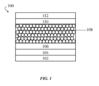
According to some embodiments, the IR photodetector has a standard, or
regular,
architecture. An exemplary schematic illustration of an IR photodetector
having a standard
architecture is shown in FIG. 1. In FIG. 1, IR photodetector 100 is a multi-
layered structure
comprising substrate 102, anode 104, optional electron blocking layer 106,
monodisperse, IR-
absorbing nanoparticle layer 108, optional hole blocking layer 110, and
cathode 112. As
shown in FIG. 1, anode 104 may be positioned adjacent substrate 102, and
optional electron
blocking layer 106 may be positioned adjacent anode 104. Cathode 112 may be
positioned
on the opposite end of IR photodetector 100, and optional hole blocking layer
110 may be
positioned adjacent cathode 112. Monodisperse, IR-absorbing nanoparticle layer
108 may be
positioned between optional electron blocking layer 106, on a first side, and
optional hole
blocking layer 110, on a second, substantially opposite side. As used herein,
when a layer is
referred to as being "on," "on top of," or "adjacent" another layer, it can be
directly on, on
top of, or adjacent the layer, or an intervening layer may also be present. A
layer that is
"directly on," "directly adjacent," or "in contact with" another layer means
that no
intervening layer is present. Likewise, a layer that is positioned "between"
two layers may be
directly between the two layers such that no intervening layer is present, or
an intervening
layer may be present.
In operation, a reverse bias voltage may be applied to photodetector 100. IR
radiation
may enter photodetector 100 through substrate 102 and pass through anode 104
and optional
CA 02988784 2017-12-07
WO 2017/039774 - 25 -
PCT/US2016/037056
electron blocking layer 106. The IR radiation may then excite electrons in
monodisperse, IR-
absorbing nanoparticle layer 108, resulting in the generation of electron-hole
pairs (e.g.,
excitons). The electrons may be transported through optional hole blocking
layer 110 to
cathode 112, while the holes may be transported through optional electron
blocking layer 106
to anode 104, thereby producing a measureable photocurrent.
In some embodiments, the reverse bias voltage applied to the photodetector may
be
relatively low. In some cases, the magnitude of the reverse bias voltage may
be about 10 V
or less, about 5 V or less, about 4 V or less, about 3 V or less, about 2 V or
less, or about 1 V
or less. In some embodiments, the magnitude of the reverse bias voltage may be
in the range
of about 0 V to about 1 V, about 0 V to about 2 V, about 0 V to about 3 V,
about 0 V to about
4 V, about 0 V to about 5 V, about 0 V to about 10 V, about 1 V to about 2 V,
about 1 V to
about 3 V, about 1 V to about 4 V, about 1 V to about 5 V, about 1 V to about
10 V, about 2
V to about 3 V, about 2 V to about 4 V, about 2 V to about 5 V, about 2 V to
about 10 V, or
about 5 V to about 10 V.
As shown in FIG. 1, IR photodetector 100 may optionally comprise hole blocking
layer 110. A hole blocking layer (HBL) generally refers to a layer that
inhibits transport of
holes between two or more layers of a device. In some cases, it may be
advantageous to
inhibit transport of holes from one layer to another because inhibiting such
transport may
reduce dark current (e.g., current that flows through a device in the absence
of IR absorption
by the monodisperse nanoparticle layer). For example, reducing dark current
may result in
enhanced performance characteristics (e.g., higher detectivity) of the IR
photodetector.
In some cases, hole blocking layer 110 may inhibit transport of holes from
cathode
112 to monodisperse, 1R-absorbing nanoparticle layer 108 under reverse bias
because there is
a substantially large gap between the work function of cathode 112 and the
valence band
energy of hole blocking layer 110. For example, the magnitude of the
difference between the
work function of the cathode and the valence band energy of the hole blocking
layer may be
at least about 0.5 eV, at least about 1 eV, at least about 1.5 eV, at least
about 2 eV, at least
about 2.5 eV, at least about 3 eV, at least about 4 eV, or at least about 5
eV. In some cases,
the magnitude of the difference between the work function of the cathode and
the valence
band energy of the hole blocking layer is in the range of about 0.5 eV to
about 1 eV, about
0.5 eV to about 1.5 eV, about 0.5 eV to about 2 eV, about 0.5 eV to about 2.5
eV, about 0.5
eV to about 3 eV, about 0.5 eV to about 4 eV, about 0.5 eV to about 5 eV,
about 1 eV to
about 2 eV, about 1 eV to about 2.5 eV, about 1 eV to about 3 eV, about 1 eV
to about 4 eV,
CA 02988784 2017-12-07
WO 2017/039774 - 26 -
PCT/US2016/037056
about leV to about 5 eV, about 1.5 eV to about 2.5 eV, about 1.5 eV to about 3
eV, about 1.5
eV to about 4 eV, about 1.5 eV to about 5 eV, about 2 eV to about 3 eV, about
2 eV to about
4 eV, or about 2 eV to about 5 eV.
In some embodiments, the valence band energy of the hole blocking layer is
relatively
high. For example, the magnitude of the valence band energy of the hole
blocking layer may
be at least about 5 eV, at least about 5.5 eV, at least about 6 eV, at least
about 6.5 eV, at least
about 7 eV, at least about 7.5 eV, at least about 8 eV, at least about 9 eV,
or at least about 10
eV. In some cases, the magnitude of the valence band energy of the hole
blocking layer is in
the range of about 5 eV to about 6 eV, about 5 eV to about 7 eV, about 5 eV to
about 8 eV,
about 5 eV to about 9 eV, about 5 eV to about 10 eV, about 6 eV to about 7 eV,
about 6 eV to
about 8 eV, about 6 eV to about 9 eV, about 6 eV to about 10 eV, about 7 eV to
about 8 eV,
about 7 eV to about 9 eV, about 7 eV to about 10 eV, about 8 eV to about 9 eV,
or about 8
eV to about 10 eV.
In certain embodiments, the hole blocking layer comprises an organic material.
Non-
limiting examples of suitable organic materials for the HBL include 2,9-
dimethy1-4,7-
dipheny1-1,10-phenanthroline (BCP), p-bis(triphenylsilyl)benzene (UGH2), 4,7-
diphenyl-
1,10-phenanthroline (BPhen), tris-(8-hydroxy quinolone) aluminum (A1q3), 3,5'-
N,N'-
dicarbazole-benzene (mCP), C60, and tris[3-(3-pyridy1)-mesityl]borane
(3TPYMB). In some
embodiments, the hole blocking layer comprises an inorganic material. Non-
limiting
examples of suitable inorganic materials for the HBL include zinc oxide (Zn0),
titanium
dioxide (Ti02), silicon monoxide (Si0), silicon dioxide (Si02), silicon
nitride (Si3N4), and
alumina (A1203). In certain cases, the HBL comprises a layer of nanoparticles.
As shown in FIG. 1, IR photodetector 100 may optionally comprise electron
blocking
layer 106. An electron blocking layer (EBL) generally refers to a layer that
inhibits transport
of electrons between two or more layers of a device. In some cases, it may be
advantageous
to inhibit transport of electrons from one layer to another because inhibiting
such transport
may reduce dark current. As noted above, reducing dark current may
advantageously
improve certain performance characteristics of the IR photodetector.
In some cases, EBL 106 may inhibit transport of electrons from anode 104 to
monodisperse, IR-absorbing nanoparticle layer 108 under reverse bias because
there is a
substantially large gap between the work function of anode 104 and the
conduction band
energy of electron blocking layer 108. For example, the magnitude of the
difference between
the work function of the anode and the conduction band energy of the electron
blocking layer
CA 02988784 2017-12-07
WO 2017/039774 - 27 -
PCT/US2016/037056
may be at least about 0.5 eV, at least about 1 eV, at least about 1.5 eV, at
least about 2 eV, at
least about 2.5 eV, at least about 3 eV, at least about 4 eV, or at least
about 5 eV. In some
cases, the magnitude of the difference between the work function of the anode
and the
conduction band energy of the electron blocking layer may be in the range of
about 0.5 eV to
about 1 eV, about 0.5 eV to about 1.5 eV, about 0.5 eV to about 2 eV, about
0.5 eV to about
2.5 eV, about 0.5 eV to about 3 eV, about 0.5 eV to about 4 eV, about 0.5 eV
to about 5 eV,
about 1 eV to about 2 eV, about 1 eV to about 2.5 eV, about 1 eV to about 3
eV, about 1 eV
to about 4 eV, about leV to about 5 eV, about 1.5 eV to about 2.5 eV, about
1.5 eV to about
3 eV, about 1.5 eV to about 4 eV, about 1.5 eV to about 5 eV, about 2 eV to
about 3 eV,
about 2 eV to about 4 eV, or about 2 eV to about 5 eV.
In certain embodiments, the conduction band energy of the electron blocking
layer
may be relatively low. In some cases, the magnitude of the conduction band
energy of the
electron blocking layer is about 3 eV or less, about 2.5 eV or less, about 2
eV or less, about
1.5 eV or less, about 1 eV or less, or about 0.5 eV or less. In some cases,
the magnitude of
the conduction band energy of the electron blocking layer is in the range of
about 0.5 eV to
about 1 eV, about 0.5 eV to about 1.5 eV, about 0.5 eV to about 2 eV, about
0.5 eV to about
2.5 eV, about 0.5 eV to about 3 eV, about 1 eV to about 1.5 eV, about 1 eV to
about 2 eV,
about 1 eV to about 2.5 eV, about 1 eV to about 3 eV, about 1.5 eV to about 2
eV, about 1.5
eV to about 2.5 eV, about 1.5 eV to about 3 eV, about 2 eV to about 2.5 eV, or
about 2.5 eV
to about 3 eV.
In some embodiments, the electron blocking layer comprises an organic
material.
Non-limiting examples of suitable organic materials for the EBL include 1,1-
bis[(di-4-
tolylamino)phenyl]cyclohexane (TAPC), N,N'-diphenyl-N,N'(2-naphthyl)-(1,1'-
pheny1)-
4,4'-diamine (NPB), N,N'-diphenyl-N,N'-di(m-tolyl)benzidine (TPD), poly(9,9-
dioctyl-
fluorene-co-N-(4-butylphenyl)diphenylamine) (TPB), poly-N,N-bis-4-butylphenyl-
N,N-bis-
phenylbenzidine (poly-TPD), and polystyrene-N,N-diphenyl-N,N-bis(4-n-
butylpheny1)-
(1,10-bipheny1)-4,4-diamine-perfluorocyclobutane (PS-TPD-PFCB). In some
embodiments,
the electron blocking layer comprises an inorganic material. Non-limiting
examples of
suitable inorganic materials for the EBL include NiO and CuO. In certain
cases, the EBL
comprises a layer of nanoparticles.
As shown in FIG. 1, IR photodetector 100 may have a standard architecture. In
some
embodiments, substrate 102 is sufficiently transparent to IR radiation to
allow IR radiation to
be detected by monodisperse, IR-absorbing nanoparticle layer 108. Examples of
suitable
CA 02988784 2017-12-07
WO 2017/039774 - 28 -
PCT/US2016/037056
materials for substrate 102 include, but are not limited to, glass, plastic,
and quartz. As
shown in FIG. 1, anode 104 may be positioned adjacent substrate 102. In some
cases, anode
104 is also transparent to IR radiation. Non-limiting examples of suitable
materials for the
anode include indium tin oxide (no), indium zinc oxide (IZO), aluminum tin
oxide (ATO),
aluminum zinc oxide (AZO), any other suitable transparent conductive oxide,
carbon
nanotubes, silver nanowires, and combinations thereof. FIG. 1 also shows that
IR
photodetector 100 may comprise cathode 112. Cathode 112 may not necessarily be
transparent to IR radiation. Examples of suitable materials for the cathode
include, but are
not limited to, Ca, Mg, Al, Ag, Au, Ti, W, LiF/A1, Ca:Mg, LiF/Al/ITO, Ag/ITO,
CsCO3/ITO,
Ba/A1, and combinations thereof. In some embodiments, the cathode may be
highly
reflective.
Alternatively, in some embodiments, the IR photodetector has an inverted
architecture
(not shown). In an inverted architecture, the cathode may be positioned
adjacent the
substrate. Accordingly, in an IR photodetector having an inverted
architecture, the cathode
may be transparent to IR radiation. Non-limiting examples of suitable
materials for the
cathode include indium tin oxide (no), magnesium, calcium, aluminum, silver,
and
combinations thereof. Conversely, the anode may not necessarily be transparent
to IR
radiation. Non-limiting examples of suitable materials for the anode include
gold, silver,
platinum, magnesium, calcium, and combinations thereof, in addition to the
anode materials
listed above.
Those of ordinary skill in the art can readily identify appropriate
combinations of
anodes, cathodes, hole blocking layers, electron blocking layers, and other
layers by their
relative work functions, valence band energies, conduction band energies,
layer
compatibility, and the nature of any desired deposition methods used during
their fabrication.
In some embodiments, the IR photodetectors described herein have properties
that
have been recognized as being advantageous. For example, the IR photodetectors
may
exhibit high specific detectivity, high responsivity, and/or high external
quantum efficiency
(EQE). Specific detectivity may generally refer to a figure of merit relating
to the sensitivity
of a photodetector, which it may be expressed using Equation 3:
R µIAAIT3
D* = _________________________________________ (3)
(2q/d)1/2
where R is responsivity (e.g., a measure of electrical output, such as
photocurrent, per optical
input), A is device area, B is bandwidth, Id is dark current density, and q is
elementary charge
CA 02988784 2017-12-07
WO 2017/039774 - 29 -
PCT/US2016/037056
(1.6 x 10⁻¹⁹ C). In some embodiments, an IR photodetector has a specific
detectivity of at
least about 1 x 10¹⁰ Jones, at least about 5 x 10¹⁰ Jones, at least about 1 x
1011 Jones, at least
about 5 x 10¹¹ Jones, at least about 1 x 10¹² Jones, or at least about 1.2 x
1012 Jones at a
wavelength of at least about 700 nm, at least about 1000 nm, at least about
1200 nm, at least
about 1500 nm, at least about 1800 nm, at least about 2000 nm, at least about
2500 nm, or at
least about 3000 nm.
In some embodiments, an IR photodetector may have a relatively high
responsivity.
In certain cases, the IR photodetector has a responsivity of at least about
0.05 A/W, at least
about 0.1 A/W, at least about 0.15 A/W, at least about 0.20 A/W, or at least
about 0.21 A/W
at a wavelength of at least about 700 nm, at least about 1000 nm, at least
about 1200 nm, at
least about 1500 nm, at least about 1800 nm, at least about 2000 nm, at least
about 2500 nm,
or at least about 3000 nm.
In some embodiments, an IR photodetector may have a relatively high external
quantum efficiency (EQE). EQE generally refers to the ratio of the number of
free charge
carriers generated to the number of incident photons on the photodetector. In
certain cases,
the IR photodetector has an EQE of at least about 1%, at least about 2%, at
least about 5%, at
least about 6%, at least about 7%, at least about 8%, at least about 9%, at
least about 10%, at
least about 15%, at least about 20%, at least about 30%, at least about 40%,
or at least about
50% at a wavelength of at least about 700 nm, at least about 1000 nm, at least
about 1200 nm,
at least about 1500 nm, at least about 1800 nm, at least about 2000 nm, at
least about 2500
nm, or at least about 3000 nm.
In some embodiments, performance of the IR photodetector may be stable in air
over
relatively long periods of time. In certain cases, the specific detectivity,
responsivity, and/or
EQE of the photodetector at a wavelength of at least about 700 nm, at least
about 1000 nm, at
least about 1200 nm, at least about 1500 nm, at least about 1800 nm, at least
about 2000 nm,
at least about 2500 nm, or at least about 3000 nm may be stable (e.g.,
changing by no more
than about 20% or less, about 10% or less, about 5% or less, or about 1% or
less) over a
period of at least about 1 day, at least about 10 days, at least about 30
days, at least about 60
days, at least about 90 days, or at least about 100 days.
In some embodiments, the IR-absorbing device is an IR up-conversion device. An
IR
up-conversion device generally refers to a device capable of absorbing IR
radiation at a first
wavelength and emitting radiation having a second, smaller wavelength (e.g.,
higher energy).
For example, an IR-to-visible up-conversion device may absorb IR radiation and
emit visible
CA 02988784 2017-12-07
WO 2017/039774 - 30 -
PCT/US2016/037056
light. In some embodiments, the up-conversion device comprises an IR-absorbing
layer
comprising the monodisperse nanoparticles described herein and a light-
emitting layer. In
certain cases, the up-conversion device comprises an IR photodetector
integrated with a light-
emitting diode (LED) (e.g., an organic light-emitting diode (OLED)). In some
embodiments,
the LED may be a multi-layered structure comprising a light-emitting layer, a
hole transport
layer (HTL), and an electron transport layer (ETL). In certain embodiments,
the up-
conversion device may further comprise a hole blocking layer (HBL) and/or an
electron
blocking layer (EBL).
FIG. 2 shows an exemplary schematic illustration of IR up-conversion device
200. IR
up-conversion device 200 comprises substrate 202, anode 204, optional hole
blocking layer
206, monodisperse, IR-absorbing nanoparticle layer 208, hole transport layer
210, light-
emitting layer 212, electron transport layer 214, and cathode 216. As shown in
FIG. 2, anode
204 may be positioned adjacent substrate 202, and optional hole blocking layer
206 may be
positioned adjacent anode 204. A first side of monodisperse, IR-absorbing
nanoparticle layer
208 may be positioned adjacent optional hole blocking layer 206. A second,
substantially
opposite side of nanoparticle layer 208 may be positioned adjacent an LED
(e.g., an OLED)
comprising light-emitting layer 212 positioned between hole transport layer
210 and electron
transport layer 214. In particular, nanoparticle layer 208 may be positioned
adjacent hole
transport layer 210. Electron transport layer 214 may be positioned adjacent
cathode 216.
In operation, a potential may be applied between anode 204 and cathode 216. IR
radiation incident on substrate 202 may pass through anode 204 and optional
hole blocking
layer 206 to monodisperse, IR-absorbing nanoparticle layer 208, which may
generate
electron-hole pairs. Holes may be transported through hole transport layer 210
to light-
emitting layer 212, where holes may combine with electrons injected from
cathode 216 and
passing through electron transport layer 214. As the holes and electrons
combine, light-
emitting layer 212 may emit visible light.
As shown in FIG. 2, IR up-conversion device 200 may comprise light-emitting
layer
212. In some embodiments, the light-emitting layer may emit visible light
(e.g.,
electromagnetic radiation having a wavelength between about 400 nm and about
700 nm).
The light-emitting layer may emit light in any portion of the visible spectrum
(e.g.,
substantially red light, substantially green light, substantially blue light).
Non-limiting
examples of suitable materials for the light-emitting layer include A1q3; fac-
tris(2-
phenylpyridinato)iridium(III) ("Ir(ppy)3"); iridium (III) bis[(4,6-di-
fluoropheny1)-pyridinate-
CA 02988784 2017-12-07
WO 2017/039774 - 31 -
PCT/US2016/037056
N,C2Thicolinate ("FIrpic"); 3,5'-N,N'-dicarbazole-benzene ("mCP") doped with
tris(2-
phenylisoquinoline)iridium ("Ir(piq)3"); mCP doped with Ir(ppy)3; mCP: FIrpic;
tra-(2-
phenylpyridine) iridium; and poly- [2-methoxy-5-(2'-ethyl-hexyloxy) phenylene
vinylene]
("MEH-PPV").
In some embodiments, IR up-conversion device 200 comprises hole transport
layer
(HTL) 210. A hole transport layer (HTL) generally refers to a layer that
facilitates hole
transport between two or more layers of a device. In some embodiments, the HTL
comprises
an organic material. Non-limiting examples of suitable organic materials for
the HTL include
1,1-bis[(di-4-tolylamino)phenyl]cyclohexane (TAPC), N,N'-diphenyl-N,N'(2-
naphthyl)-(1,1'-
phenyl)-4,4'-diamine (NPB), and N,N'-diphenyl-N,N'-di(m-tolyl)benzidine (TPD).
In some cases, HTL 210 facilitates transport of holes from monodisperse, IR-
absorbing nanoparticle layer 208 to light-emitting layer 212. HTL 210 may
facilitate
transport of holes from monodisperse, IR-absorbing nanoparticle layer 208
because the
valence band energy of HTL 210 is substantially aligned with the valence band
energy of
monodisperse, IR-absorbing nanoparticle layer 208. For example, in certain
embodiments,
the magnitude of the difference between the valence band energy of HTL 210 and
the valence
band energy of monodisperse, IR-absorbing nanoparticle layer 208 is about 1 eV
or less,
about 0.8 eV or less, about 0.6 eV or less, about 0.5 eV or less, about 0.4 eV
or less, about 0.3
eV or less, about 0.25 eV or less, about 0.2 eV or less, about 0.15 eV or
less, about 0.1 eV or
less, or about 0.05 eV or less. In some cases, the magnitude of the difference
between the
valence band energy of HTL 210 and the valence band energy of monodisperse, IR-
absorbing
nanoparticle layer 208 is in the range of about 0.05 eV to about 0.1 eV, about
0.05 eV to
about 0.2 eV, about 0.05 eV to about 0.3 eV, about 0.05 eV to about 0.4 eV,
about 0.05 eV to
about 0.5 eV, about 0.05 eV to about 1 eV, about 0.1 eV to about 0.2 eV, about
0.1 eV to
about 0.3 eV, about 0.1 eV to about 0.4 eV, about 0.1 eV to about 0.5 eV,
about 0.1 eV to
about 1 eV, about 0.2 eV to about 0.3 eV, about 0.2 eV to about 0.4 eV, about
0.2 eV to
about 0.5 eV, or about 0.2 eV to about 1 eV.
In some cases, hole transport layer 210 may facilitate transport of holes to
light-
emitting layer 212 because the valence band energy of HTL 210 is substantially
aligned with
the valence band energy of light-emitting layer 212. For example, the
magnitude of the
difference between the valence band energy of HTL 210 and the valence band
energy of
light-emitting layer 212 may be about 1 eV or less, about 0.8 eV or less,
about 0.6 eV or less,
about 0.5 eV or less, about 0.4 eV or less, about 0.3 eV or less, about 0.25
eV or less, about
CA 02988784 2017-12-07
WO 2017/039774 - 32 -
PCT/US2016/037056
0.2 eV or less, about 0.15 eV or less, about 0.1 eV or less, or about 0.05 eV
or less. In some
cases, the magnitude of the difference between the valence band energy of HTL
210 and the
valence band energy of light-emitting layer 212 is in the range of about 0.05
eV to about 0.1
eV, about 0.05 eV to about 0.2 eV, about 0.05 eV to about 0.3 eV, about 0.05
eV to about 0.4
eV, about 0.05 eV to about 0.5 eV, about 0.05 eV to about 1 eV, about 0.1 eV
to about 0.2
eV, about 0.1 eV to about 0.3 eV, about 0.1 eV to about 0.4 eV, about 0.1 eV
to about 0.5 eV,
about 0.1 eV to about 1 eV, about 0.2 eV to about 0.3 eV, about 0.2 eV to
about 0.4 eV,
about 0.2 eV to about 0.5 eV, or about 0.2 eV to about 1 eV.
In some embodiments, IR up-conversion device 200 comprises electron transport
layer (ETL) 214. An electron transport layer generally refers to a layer that
facilitates
electron transport between two or more layers of a device. In some
embodiments, the ETL
comprises an organic material. Non-limiting examples of suitable organic
materials include
tris[3-(3-pyridy1)-mesityl]borane (3TPYMB), 2,9-dimethy1-4,7-dipheny1-1,10-
phenanthroline
(BCP), 4,7-dipheny1-1,10-phenanthroline (BPhen), and tris-(8-hydroxy
quinoline) aluminum
(Alq3).
In some cases, ETL 214 facilitates transport of electrons from cathode 216 to
light-
emitting layer 212. ETL 214 may facilitate transport of electrons from cathode
216 because
the conduction band energy of ETL 214 is substantially aligned with the work
function of
cathode 216. For example, the magnitude of the difference between the work
function of
cathode 216 and the conduction band energy of ETL 214 may be about 1 eV or
less, about
0.8 eV or less, about 0.6 eV or less, about 0.5 eV or less, about 0.4 eV or
less, about 0.3 eV
or less, about 0.25 eV or less, about 0.2 eV or less, about 0.15 eV or less,
about 0.1 eV or
less, or about 0.05 eV or less. In some cases, the magnitude of the difference
between the
work function of cathode 216 and the conduction band energy of ETL 214 may be
in the
range of about 0.05 eV to about 0.1 eV, about 0.05 eV to about 0.2 eV, about
0.05 eV to
about 0.3 eV, about 0.05 eV to about 0.4 eV, about 0.05 eV to about 0.5 eV,
about 0.05 eV to
about 1 eV, about 0.1 eV to about 0.2 eV, about 0.1 eV to about 0.3 eV, about
0.1 eV to
about 0.4 eV, about 0.1 eV to about 0.5 eV, about 0.1 eV to about 1 eV, about
0.2 eV to
about 0.3 eV, about 0.2 eV to about 0.4 eV, about 0.2 eV to about 0.5 eV, or
about 0.2 eV to
about 1 eV.
In some embodiments, ETL 214 may facilitate electron transport to light-
emitting
layer 212 because the conduction band energy of ETL 214 is substantially
aligned with the
conduction band energy of light-emitting layer 212. For example, in certain
cases, the
CA 02988784 2017-12-07
WO 2017/039774 - 33 -
PCT/US2016/037056
magnitude of the difference between the conduction band energy of light-
emitting layer 212
and the conduction band energy of ETL 214 may be about 1 eV or less, about 0.8
eV or less,
about 0.6 eV or less, about 0.5 eV or less, about 0.4 eV or less, about 0.3 eV
or less, about
0.25 eV or less, about 0.2 eV or less, about 0.15 eV or less, about 0.1 eV or
less, or about
0.05 eV or less. In some cases, the magnitude of the difference between the
conduction band
energy of light-emitting layer 212 and the conduction band energy of ETL 214
may be in the
range of about 0.05 eV to about 0.1 eV, about 0.05 eV to about 0.2 eV, about
0.05 eV to
about 0.3 eV, about 0.05 eV to about 0.4 eV, about 0.05 eV to about 0.5 eV,
about 0.05 eV to
about 1 eV, about 0.1 eV to about 0.2 eV, about 0.1 eV to about 0.3 eV, about
0.1 eV to
about 0.4 eV, about 0.1 eV to about 0.5 eV, about 0.1 eV to about 1 eV, about
0.2 eV to
about 0.3 eV, about 0.2 eV to about 0.4 eV, about 0.2 eV to about 0.5 eV, or
about 0.2 eV to
about 1 eV.
In some embodiments, the IR up-conversion device may further comprise an
anode, a
cathode, a hole blocking layer, an electron blocking layer, and/or a
substrate. One of
ordinary skill in the art would be able to identify appropriate materials for
each layer based
on the above disclosure. Additionally, it is noted that while FIG. 2 shows IR
up-conversion
device 200 having a standard architecture, the IR up-conversion device may
instead have an
inverted architecture in which the cathode is positioned adjacent the
substrate.
In some embodiments, the IR-absorbing device is an IR solar cell (e.g., an IR
photovoltaic cell). An IR solar cell generally refers to a device capable of
absorbing IR
radiation (e.g., IR radiation emitted by the sun) and generating electricity.
In some
embodiments, an IR solar cell comprises an anode, a cathode, and an IR-
absorbing layer
comprising the monodisperse nanoparticles described herein. In addition, the
IR solar cell
may further comprise an electron extraction layer and/or a hole extraction
layer.
FIG. 3 shows an exemplary schematic illustration of IR solar cell 300. As
shown in
FIG. 3, IR solar cell 300 comprises substrate 302, anode 304, optional hole
extraction layer
306, monodisperse, IR-absorbing nanoparticle layer 308, optional electron
extraction layer
310, and cathode 312. As shown in FIG. 3, anode 304 may be positioned adjacent
substrate
302, and optional hole extraction layer 306 may be positioned adjacent anode
304. Cathode
312 may be positioned on the opposite end of IR solar cell 300, and optional
electron
extraction layer 310 may be positioned adjacent cathode 312. Monodisperse, IR-
absorbing
nanoparticle layer 308 may be positioned between optional hole extraction
layer 306, on a
first side, and optional electron extraction layer 310, on a second,
substantially opposite side.
CA 02988784 2017-12-07
WO 2017/039774 - 34 -
PCT/US2016/037056
IR solar cell 300 may be operated under a forward bias voltage or no external
bias
voltage. In operation, IR radiation may enter IR solar cell 300 through
substrate 302 and pass
through anode 304 and optional hole extraction layer 306. The IR radiation may
then excite
electrons in monodisperse, IR-absorbing nanoparticle layer 308, resulting in
the generation of
electron-hole pairs. The holes may be transported through optional hole
extracting layer 306
to anode 304, and the electrons may be transported through optional electron
extracting layer
310 to cathode 312 to produce an electric current.
In some embodiments, the IR solar cell comprises a hole extraction layer. For
example, in IR solar cell 300, hole extraction layer 306 may facilitate
transport of holes from
monodisperse, IR-absorbing nanoparticle layer 308 to anode 304. In certain
embodiments,
the hole extraction layer comprises a highly n-type material. An n-type
material generally
refers to a material having a higher concentration of electrons than holes
(e.g., the Fermi level
lies closer to the conduction band than the valence band). In some cases, the
hole extraction
layer may have a large work function (e.g., a work function substantially
aligned with the
work function of anode 304). Non-limiting examples of suitable materials for
the hole
extraction layer include molybdenum oxide (Mo03), tungsten oxide (W03), and
vanadium
oxide (V205)=
In some embodiments, the IR solar cell comprises an electron extraction layer.
For
example, in IR solar cell 300, electron extraction layer 310 may facilitate
transport of
electrons from monodisperse, IR-absorbing nanoparticle layer 308 to cathode
312. Examples
of suitable materials for the electron extraction layer include, but are not
limited to, titanium
dioxide (Ti02), zinc oxide (Zn0), lithium fluoride (LiF), lithium cobalt oxide
(LiCo02),
cesium fluoride (CsF), cesium carbonate (Cs2CO3), niobium pentoxide (Nb205),
carbon
nanotubes (CNTs), zinc tin oxide (ZTO), and polyethylene oxide (PEO).
In some embodiments, the IR up-conversion device further comprises an anode, a
cathode, and/or a substrate. One of ordinary skill in the art would be able to
identify
appropriate materials for each layer based on the above disclosure.
Additionally, it is noted
that while FIG. 3 shows IR solar cell 300 having a standard architecture, the
IR solar cell may
instead have an inverted architecture in which the cathode is positioned
adjacent the
substrate.
In some embodiments, the IR solar cells described herein have properties that
have
been recognized as being advantageous. For example, the monodisperse, IR-
absorbing
nanoparticle layers may enhance charge extraction. Accordingly, the IR solar
cells described
CA 02988784 2017-12-07
WO 2017/039774 - 35 -
PCT/US2016/037056
herein may exhibit relatively high photocurrent efficiency (PCE). PCE
generally refers to the
ratio of the number of generated charge carriers to the number of absorbed
photons. In some
embodiments, the IR solar cell has a photocurrent efficiency of at least about
1%, at least
about 2%, at least about 3%, at least about 4%, at least about 5%, at least
about 6%, at least
about 7%, at least about 8%, at least about 9%, at least about 10%, at least
about 15%, or at
least about 20% at a wavelength of at least about 700 nm, at least about 1000
nm, at least
about 1200 nm, at least about 1500 nm, at least about 1800 nm, at least about
2000 nm, at
least about 2500 nm, or at least about 3000.
In some embodiments, a solar panel comprises a plurality of IR solar cells,
where at
least a portion of the IR solar cells comprise a monodisperse, IR-absorbing
nanoparticle
layer. In certain embodiments, the solar panel comprises at least one IR solar
cell capable of
absorbing IR radiation at a first wavelength and at least one IR solar cell
capable of absorbing
IR radiation at a second, different wavelength. The solar panel may comprise
at least 2, at
least 3, at least 4, at least 5, at least 10, at least 20, at least 50, or at
least 100 IR solar cells.
In some cases, the devices described herein may be relatively thin. For
example, in
certain embodiments, a device may have a thickness of about 1 p.m or less,
about 500 nm or
less, about 200 nm or less, about 100 nm or less, about 50 nm or less, or
about 10 nm or less.
In some cases, the device may have a thickness in the range of about 10 nm to
about 50 nm,
about 10 nm to about 100 nm, about 10 nm to about 200 nm, about 10 nm to about
500 nm,
about 10 nm to about 1 p.m, about 50 nm to about 100 nm, about 50 nm to about
200 nm,
about 50 nm to about 500 nm, about 50 nm to about 1 p.m, about 100 nm to about
200 nm,
about 100 nm to about 500 nm, about 100 nm to about 1 p.m, or about 500 nm to
about 1 p.m.
EXAMPLE 1
This example describes the fabrication and characterization of monodisperse
PbS
nanocrystals (NCs).
Highly monodisperse PbS nanocrystals (NCs) with absorption peaks of more than
2000 nm were synthesized by a multiple injection method. In order to
synthesize
monodisperse NCs, nucleation was suppressed during the growth process by
controlling the
molar ratio of precursors during the multiple injections. Compared with prior
art methods,
NCs were synthesized at a lower growth temperature (105 C) within a shorter
growth time
(30 minutes).
CA 02988784 2017-12-07
WO 2017/039774 - 36 -
PCT/US2016/037056
Initially, the effect of the molar ratio of precursors during the initial
injection was
investigated. As shown in FIG. 4, the lead to sulfur (Pb:S) ratio was varied
from 2:1 to 8:1,
and absorption spectra were obtained. It was found that increasing the ratio
of lead to sulfur
resulted in a peak shift towards larger wavelengths. For example, it was found
that at a Pb:S
ratio of 2:1, a peak occurred at about 1000 nm, while at a Pb:S ratio of 8:1,
a peak occurred at
about 1600 nm. This therefore demonstrated that increasing the proportion of
Pb relative to S
resulted in highly monodisperse NCs capable of absorbing radiation at
wavelengths above
1000 nm. Without wishing to be bound by a particular theory, this may have
occurred due to
the ratio of precursors in the initial injection controlling the number of
initial nuclei that were
formed. If most of the sulfur monomers in the precursor solution were consumed
during the
initial nucleation period, there were insufficient sulfur precursor monomers
to initiate further
growth. Instead, nucleation stopped, and uniform growth of existing nuclei
began, resulting
in larger NCs that absorbed radiation having longer wavelengths.
It was recognized that the final size of the NCs was affected by the monomers
remaining after initial nucleation. In order to extend the growth period and
increase the final
size of the NCs, a multiple injection method was developed. After the first
injection
described above, additional monomers were injected such that the sulfur
concentration
remained below the threshold concentration for nucleation. As a result, the
additional sulfur
monomers were only used to grow existing NCs without further nucleation, and
PbS NCs
with diameters larger than 10 nm were grown. FIG. 5A shows absorption spectra
of PbS NCs
after one injection, two injections, three injections, and four injections.
From FIG. 5A, it can
be seen that after the first injection, a peak occurred at about 1200 nm,
after the second
injection, a peak occurred at about 1400 nm, after the third injection, a peak
occurred at about
1500 nm, and after the fourth injection, a peak occurred at about 1600 nm.
This
demonstrated that further injections increased the size of PbS NCs, leading to
absorption of
radiation having larger wavelengths. This can be further seen from FIG. 5B,
which
demonstrated that increasing numbers of bis(trimethylsilyl)sulfide ("TMS")
injections, and
concomitantly increasing the volume of quantum dots, resulted in absorption of
radiation at
increasing wavelengths. The optical absorption spectra in FIG. 5A also
demonstrated the
monodispersity of the PbS NCs.
With good control of initial nucleation and growth, large PbS NCs with an
absorption
peak of more than 2000 nm were grown. FIG. 6A shows absorption spectra of
different sized
PbS NCs in tetrachloroethylene (TCE). As demonstrated by FIG. 6A, PbS NCs
synthesized
CA 02988784 2017-12-07
WO 2017/039774 - 37 -
PCT/US2016/037056
by a multiple injection method were tuned from about 1.36 eV (913 nm) to about
0.59 eV
(2085 nm). It was observed that the size distribution of NCs synthesized at
low temperatures
was much narrower than the size distribution of NCs synthesized at high
temperatures. FIG.
6B also demonstrated that as the number of bis(trimethylsilyl)sulfide ("TMS")
injections
increased, and the volume of quantum dots accordingly increased, the radiation
absorbed had
longer wavelengths.
The reproducibility of synthesis of PbS NCs using the method described in this
example was demonstrated. FIG. 7 shows plots of absorption spectra for PbS NCs
synthesized in three different batches. It was found that the absorption
spectra all exhibited a
peak in the same location. This demonstrated that synthesis of NCs was highly
reproducible
and that the NCs were suitable for device applications.
A photodetector was fabricated with the monodisperse PbS NCs synthesized
according to the multiple injection method. The photodetector comprised an ITO
electrode, a
ZnO hole blocking layer, a layer of PbS quantum dots, a hole transport layer
comprising
NPB, and a Mo03 layer. It was found that the photodetector had an IR response
of more than
2000 nm. FIG. 8A shows the absorbance spectrum of the PbS NCs used in the
photodetector.
A schematic of the energy band structure of the photodetector is shown in the
inset of FIG.
8A. A photoresponse under IR illumination at 1800 nm was demonstrated, and the
external
quantum efficiency at 1800 nm was found to be 6.5%. The detectivity at 1800 nm
was found
to be lx1011 Jones. A photoresponse under IR illumination at 1950 nm was also
clearly
demonstrated. FIG. 8B shows the current-voltage (I-V) characteristics of the
photodetector in
the dark and under IR illumination at a peak absorption wavelength of 1950 nm.
EXAMPLE 2
This Example describes the synthesis of large, monodisperse PbS NCs and the
use of
the NCs in a multi-spectral photodetector.
Visible and infrared (IR) photodetectors are widely used in optical
communications,
imaging, security, ranging, and consumer electronics. While silicon (Si)
photodetectors are
excellent in the visible and near IR regions, they generally have low
sensitivity beyond 1000
nm. For sensing in the short-wave IR (SWIR) wavelength region (up to 1700 nm),
InGaAs
photodetectors are typically used. However, InGaAs image sensors are expensive
because of
the epitaxial process used to grow these materials, and they can only be used
in the NIR and
CA 02988784 2017-12-07
WO 2017/039774 - 38 -
PCT/US2016/037056
SWIR spectral regions. It is desirable to have a multi-spectral sensor with
good wavelength
sensitivity from 350 nm to 2000 nm.
PbS nanocrystals (NCs) with excellent photosensitivity, bandgap tunability,
and
solution processability provide an attractive platform for low-cost multi-
spectral
photodetectors with light sensitivity from the UV/Visible to SWIR (350-2000
nm) spectral
regions. However, while there have been numerous reports of devices using PbS
NCs as the
IR sensitizing layer, most PbS NC devices have limited IR sensitivity beyond
1300 nm
because of the challenges associated with synthesis of large PbS NCs. For
example, PbS
NCs with an absorption peak at 2000 nm have a volume 7 times the volume of NCs
with an
absorption peak at 1200 nm, as shown in FIG. 9, thus requiring a significant
increase in the
growth volume of the NCs. To synthesize large-size NCs, high growth
temperatures and long
growth times are typically used, leading to a high defect density and a large
particle size
dispersion due to uncontrollable nucleation and Ostwald ripening during
growth. For
example, in one study, PbS NCs with a diameter greater than 9.6 nm and
absorption peaks
longer than 2000 nm were synthesized. However, these large NCs were
synthesized with a
growth time longer than 120 minutes at a high growth temperature higher than
160 C, which
resulted in a size dispersion larger than 20%. Because of the energetics of
highly dispersed
PbS NCs, they lead to charge trapping and poor charge extraction in devices.
In this Example, solution-processed inorganic UV-Visible-SWIR photodetectors
with
light sensitivity from 350 nm to 2000 nm were fabricated using highly
monodisperse (less
than about 4%) PbS NCs with an NC size larger than 8.2 nm, corresponding to an
absorption
peak of 1800 nm. The monodisperse NCs were synthesized by multiple injections
of a sulfur
precursor at a low growth temperature (100 C) with a short growth time (less
than 50
minutes). To achieve facile size control with high monodispersity, the growth
process was
separated from nucleation and was done by controlling the molar ratio of lead
oxide (Pb0) as
the lead precursor and bis(trimethylsilyl)sulfide R(CH3)3Si)2S] (sometimes
referred to as
"TMS") as the sulfur precursor. Initial nucleation was controlled by the first
injection of
bis(trimethylsilyl)sulfide, and growth of the NCs was attained by subsequent
multiple
injections of bis(trimethylsilyl)sulfide. This method enabled PbS NC synthesis
with excellent
particle size control, resulting in well-defined absorption peaks at longer
wavelengths and
highly reproducible growth. Additionally, these NCs were very stable, and the
resulting
devices exhibited very good stability even without encapsulation.
CA 02988784 2017-12-07
WO 2017/039774 - 39 -
PCT/US2016/037056
A typical hot injection method was modified for the PbS NC synthesis, in which
the
sulfur precursor solution [bis(trimethylsilyl)sulfide dissolved in octadecene]
was rapidly
injected into the lead precursor solution (Pb0 dissolved in a mixture of
octadecene and oleic
acid) under constant Ar flow with vigorous stirring. In previous hot injection
PbS NC
syntheses, nucleation and growth processes could not be separated, and growth
of larger NCs
required Ostwald ripening, resulting in a large size dispersion. To separate
the growth
process from nucleation, a multiple injection method for PbS NCs was
developed. After the
first injection of sulfur monomers for nucleation, additional injections
supplied sufficient
monomers for the growth of PbS NCs with diameters larger than 9.6 nm. In order
to avoid
large particle size distribution during the additional injection cycles, the
lead precursors were
diluted in non-coordinating solvents such as oleic acid (OA) and octadecene
(ODE), such that
there was no Ostwald ripening during the synthesis of NCs. This resulted in
suppression of
particle coarsening and particle size dispersion. As shown in FIG. 10, with
this strategy, the
initial growth was well controlled, and the seed NCs grown during the first
injection with
reaction times from 6 min to 60 min had identical absorption peaks.
To grow the NCs (i.e., increase their size), a multiple injection method of
the
bis(trimethylsilyl)sulfide solution was implemented as shown in FIG. 11.
Nucleation began
when the sulfur precursor concentration exceeded the nucleation threshold and
stopped as the
concentration was depleted below the threshold. The strategy that was adopted
was to
control the sulfur concentration below the nucleation threshold during
subsequent injections
such that the additional sulfur precursor only contributed to the growth of
the NCs without
further nucleation. Thus, the final NC size was determined by the amount of
sulfur precusor
added during subsequent injections. Using this method, highly monodisperse NCs
with a
diameter larger than 9 nm were consistently grown. FIG. 12 shows the
absorption spectra of
PbS NCs synthesized with 1 ¨ 9 bis(trimethylsilyl)sulfide injections and
demonstrates very
well-controlled NC size. To demonstrate that all subsequent
bis(trimethylsilyl)sulfide
injections after the first bis(trimethylsilyl)sulfide injection only
contributed to NC growth,
FIG. 13 shows the dependence of the volumes of the synthesized NCs on the
volumes of the
injected sulfur precursor. In FIG. 13, the volume of the synthesized NCs is
proportional to
the volume of additional injected sulfur precursor with a slope of 1,
indicating that additional
sulfur precursor injections were consumed for growth only.
With this good control of nucleation and growth, large PbS NCs with an
absorption
peak at 2000 nm were synthesized. FIG. 14 shows the absorption spectra of PbS
NCs with
CA 02988784 2017-12-07
WO 2017/039774 - 40 -
PCT/US2016/037056
different sizes from 3.9 nm to 9.6 nm, corresponding to absorption peak
wavelengths from
920 nm to 2000 nm, respectively. The multiple injection method resulted in
highly
monodisperse size distributions, even with a particle size larger than 9.6 nm.
As shown in
FIG. 15, there was no increase in size dispersion with increasing NC size, and
the NC size
dispersion values were below 6%. The reproducibility of the PbS NC synthesis
using the
multiple injection method was also confirmed. Three separate PbS NCs syntheses
gave the
same NC size and dispersion, showing that the batch-to-batch variation was
very small. This
excellent reproducibility demonstrated the suitability of these NCs for device
fabrication.
A multi-spectral photodetector was fabricated using the highly monodisperse
NCs
synthesized via the multiple injection method, with a layer of the highly
monodisperse NCs
sandwiched between colloidal ZnO nanoparticles as the electron transport/hole
blocking layer
(ETL/HBL) and solution-derived NiO as the hole transport/electron blocking
layer
(HTL/EBL). This formed a P-I-N-like photodiode structure with a low dark
current, despite
the narrow bandgap of the PbS NC photoactive layer. FIG. 16 shows the
absorption
spectrum of the PbS NCs used in the photodetector, and the inset of FIG. 16
shows a
transmission electron microscopy (TEM) image of the NCs that confirms that the
PbS NCs
were highly monodisperse. FIG. 17 shows the current-voltage (J-V)
characteristics of the
photodiode in the dark and under IR illumination at 2\., = 1800 nm with a
power density of 140
IIW/cm2. The schematic energy band diagram of the photodetector is shown in
the inset of
FIG. 17.
The photodetector exhibited typical rectifying characteristics of a diode,
with a
rectification ratio of about 1 x 10³ ( 0.5 V). The photodiode showed low dark
currents of
4x10⁻⁶ mA/cm2 at 0 V and 2x10⁻³ mA/cm2 at -1 V. FIG. 18 shows the responsivity
spectra at
0 V and -0.5 V. The responsivity spectra were similar to the absorption
spectra of the PbS
NCs, showing a peak wavelength of 1800 nm. The responsivity values at a
reverse bias of -
0.5 V were in the range of 0.05-0.21 A/W, corresponding to external quantum
efficiencies of
1 ¨ 50 %, over the entire wavelength range of 350 nm to 2000 nm. At the
absorption
maximum of 1800, responsivity reached a value of 0.21 A/W. These responsivity
values
were on the same order of magnitude as the values reported for commercially
available
photodiodes. The figure of merit for a photodetector is the specific
detectivity (D*), which
can be determined according to Equation 4:
D = (A )' 2 R Ii
" (4)
where A is the area of the detector in cm2, Af is the bandwidth in Hz, R is
the corresponding
CA 02988784 2017-12-07
WO 2017/039774 - 41 -
PCT/US2016/037056
responsivity in A/W, and in is the noise current in A. Using the measured
values of noise
current and responsivity, detectivity spectra of the multi-spectral
photodetector with large
PbS NCs were obtained. The detectivity spectra of the PbS NC device (and an
InGaAs
device for comparison) are shown in FIG. 19. The detectivity spectrum of the
PbS NC device
was similar to the absorption spectrum of the PbS NC device, showing a peak
wavelength of
1800 nm. The detectivity values of the PbS NC device were over 1 x10¹¹ Jones
for UV-
Visible-SWIR wavelengths from 350 nm to 2000 nm, and the maximum detectivity
value
was 1.2x10¹² Jones at the peak wavelength of 1800 nm, despite the narrow
bandgap of the
large PbS NCs.
To further study the effects of NC dispersity on device performance, the
following
photodetectors were fabricated using different mixtures of PbS NCs: Device 1
comprised a
mixture of PbS NCs with absorption peaks of 1470 nm and 1800 nm, and Device 2
comprised a mixture of PbS NCs with absorption peaks of 1320 nm and 1800 nm.
Device 3,
which was made with monodisperse NCs with an absorption peak at 1800 nm, was
used as a
reference. The absorption spectra of the different-sized PbS NCs are shown in
FIG. 20. In
FIG. 21A, the responsivity spectra of Devices 1, 2, and 3 at a reverse bias of
-0.5 V are
shown, and in FIG. 21B, the detectivity spectra of Devices 1, 2, and 3 at a
reverse bias of -0.5
V are shown. In the responsivity and detectivity spectra for Devices 1 and 2,
there were two
absorption peaks that corresponded to a mixture of two different sized PbS
NCs. The
responsivity values of Devices 1 and 2 at the peak wavelength of 1800 nm were
40% and
27%, respectively, of the corresponding value for the reference device (Device
3), indicating
that the photo-generated charge carrier extraction in the devices with mixed
NCs was
suppressed due to the polydispersity of the NCs. As a result, the detectivity
values of
Devices 1 and 2 at the peak wavelength of 1800 nm were 43% and 36%,
respectively, of the
corresponding value for Device 3. Furthermore, Device 2 showed a lower
responsivity and
detectivity than Device 1, indicating that a larger dispersity resulted in
stronger charge
trapping in the PbS NC layer. Therefore, the data showed the importance of
monodispersity
of NCs for optimum device performance.
To characterize the temporal response of the photodetector, the device speed
of
response was measured using a pulsed light emitting diode (LED) light source.
A rise time of
11.0 0.4 i.ts and a fall (recovery) time of 15.0 0.6 i.ts were obtained,
as shown in FIG. 22.
The corresponding bandwidth was over 10 kHz, which is sufficient for imaging
applications.
FIG. 23 shows the linearity of the photoresponse over 3 decades of power
intensity.
CA 02988784 2017-12-07
WO 2017/039774 - 42 -
PCT/US2016/037056
The storage stability of the photodetector was also measured, as shown in FIG.
24.
During the testing period of 3 months, the unencapsulated device was stored in
an ambient
environment. In the first few days of storage, the device performance actually
improved
slightly, and subsequently the device remained stable during the entire
testing period. The
initial improvement in device performance has also been reported with solution-
processed
oxide with charge blocking layers including ZnO and NiO. The air stability
data suggest that
these solution-processed UV-Visible-SWIR PbS NC-based photodetectors are very
stable.
In conclusion, solution-processed inorganic UV-Visible-SWIR photodetectors
with
light sensitivity from 350 nm to 2000 nm were fabricated using highly
monodisperse large
PbS NCs with extremely low size dispersions (less than 6%). These highly
monodisperse
large PbS NCs were synthesized by multiple injections of the sulfur precursor
solution to
grow the NCs without initiating new nucleation during growth. This method
enabled PbS
NC synthesis with excellent particle size control, resulting in well-defined
absorption peaks
at long wavelengths. The UV-Visible-SWIR multi-spectral photodetector
fabricated from
these highly monodisperse large PbS NCs showed detectivity values of over 1
x1011 Jones
from 350 nm to 2000 nm, and a maximum detectivity value of 1.2x10¹² Jones at
the peak
wavelength of 1800 nm. With a speed of response on the order of a few tens of
microseconds, the bandwidth was about 10 kHz and was sufficient for imaging
applications.
Additionally, these NCs were very stable, and the lifetime of the devices made
with these
NCs showed extremely good stability.
Experimental Section
Synthesis of PbS nanocrystals: In a typical reaction, Pb0 (0.446 g) was
dissolved in a
mixture of octadecene (50 ml) and oleic acid (3.8 ml) under a constant flow of
argon with
vigorous stirring. The mixture was heated to 100 C for about 1 hour to dry
the solution and
form lead oleate. A solution of bis(trimethylsilyl)sulfide R(CH3)3Si)2S] was
dissolved in
octadecene in the range of 0.5 mmol to 2 mmol. The solution of
bis(trimethylsilyl)sulfide
was rapidly injected into the lead oleate solution at 100 C. The addition of
bis(trimethylsilyl)sulfide raised the concentration of molecularly dissolved
sulfur above the
nucleation threshold. The rate of nucleation was controlled by the
concentration of sulfur and
surfactant (oleic acid). After the nucleation stage, the concentration of
sulfur decreased
below the critical concentration, and nucleation fell almost immediately to
zero. In order to
extend the growth period and then increase the final size of nanocrystals, a
multiple injection
method was developed. After the initial injection of
bis(trimethylsilyl)sulfide for nucleation,
CA 02988784 2017-12-07
WO 2017/039774 - 43 -
PCT/US2016/037056
additional injections of bis(trimethylsilyl)sulfide in the range of 0.1 mmol
to 0.4 mmol
supplied sufficient precursor for the growth of PbS NCs with diameters larger
than 9.6 nm.
To terminate the reaction, cold toluene was injected into the reaction
mixture. The
synthesized nanocrystals were subsequently washed via precipitation with a
polar solvent,
such as isopropanol, acetone, or methanol, and redispersed in toluene. The
washing process
was repeated three times to eliminate excess unreacted precursors and reaction
byproducts.
Synthesis of ZnO nanoparticles: The synthesis was performed by dropwise
addition of
a stoichiometric amount of tetramethylammonium hydroxide (TMAH) (0.55 M) to 30
mL of
0.1 M zinc acetate dihydrate dissolved in dimethyl sulfoxide (DMSO) under
continuous
stirring. After precipitation and washing, the nanoparticles were dispersed in
pure ethanol.
Synthesis of NiO precursors: A 0.1 M solution of nickel acetate tetrahydrate
in
ethanol was prepared. A 1:1: mole ratio of monoethanolamine (MEA) to nickel
was added as
a complexing agent, and the solution was stirred until all reagents dissolved
into a green
solution.
Device Fabrication: The NiO precursor solution was spincast onto solvent and
UV03-
cleaned ITO-coated glass substrates and heated to 500 C in air for one hour
to form
continuous NiO films. After cooling, the substrates were spincast from a
dilute suspension of
QDs in chloroform. After each layer deposition, the films were soaked in a 1.0
M solution of
1,3-benzenedithiol in acetonitrile for the ligand exchange. This PbS film
deposition and
ligand exchange procedure was repeated to yield approximately 200 nm thick
films. ZnO
nanoparticles were directly spincast on top, and the device was heated to 80
C for 15
minutes. Then a 100 nm thick aluminum cathode was thermally evaporated at
chamber
pressures of about 10-6 Ton. All layers were spincast in air.
Device Characterization: All characterization and noise measurements were
performed at room temperature. Current-voltage (J-V) characterization was
performed with a
Keithley 4200 semiconductor parameter analyzer system. EQE and responsivity
measurements were conducted using an in-house setup comprising a Xenon DC arc
lamp, an
ORIEL 74125 monochromator, a Keithley 428 current amplifier, an SR 540 chopper
system,
and an 5R830 DSP lock-in amplifier from SRS. Spectrophotometry provided a
direct
measure of the NC optical and electronic properties, including the absorption
spectra of the
NCs, the particle size, and particle size distribution. From the absorption
spectra of the
nanocrystals, the energy band gap of the nanocrystals was approximated by
calculating the
energy of the absorbed photons at the first excitonic absorption peak of the
NCs. The NC
CA 02988784 2017-12-07
WO 2017/039774 - 44 -
PCT/US2016/037056
samples were usually diluted solutions in a solvent that did not have
background absorption
interfering with the NC material, such as tetrachloroethylene (TCE). As an
alternative, the
samples may also be prepared in thin film form coated on glass substrates. The
size
distribution of the nanocrystals was defined by FWHM of the absorption spectra
of quantum
dots. A smaller FWHM corresponded to a narrower nanocrystal size distribution.
The
FWHM values of the UV-vis spectra were measured according to the following
steps. First,
a line was drawn by linking the top point of the peak to the center of the
baseline, then a line
parallel to the baseline was made through the center of the resulting line.
After that, there
were two points of intersection between the line and the peak. The wavelength
difference
between the two points was the FWHM value of the absorption peak.
Transmission electron microscopy (TEM) was performed on field emission STEM
(JEOL 2010F) operating at 200 kV. In order to determine average size and
dispersion, TEM
images were analyzed. TEM samples were prepared by dropping QDs solution in
chloroform
on the amorphous carbon film coated grids.
The noise current in the photodetector was measured using a Stanford Research
5R830 lock-in amplifier and a 5R570 low noise preamplifier. During the
measurements, the
lock-in frequency of the noise current was set to 30 Hz. In order to minimize
the noise, the
device was biased with alkaline batteries, and measurements were carried out
in an
electrically and optically shielded probe station.
While several embodiments of the present invention have been described and
illustrated herein, those of ordinary skill in the art will readily envision a
variety of other
means and/or structures for performing the functions and/or obtaining the
results and/or one
or more of the advantages described herein, and each of such variations and/or
modifications
is deemed to be within the scope of the present invention.
More generally, those skilled in the art will readily appreciate that all
parameters,
dimensions, materials, and configurations described herein are meant to be
exemplary and
that the actual parameters, dimensions, materials, and/or configurations will
depend upon the
specific application or applications for which the teachings of the present
invention is/are
used. Those skilled in the art will recognize, or be able to ascertain using
no more than
routine experimentation, many equivalents to the specific embodiments of the
invention
described herein. It is, therefore, to be understood that the foregoing
embodiments are
presented by way of example only and that, within the scope of the appended
claims and
CA 02988784 2017-12-07
WO 2017/039774 - 45 -
PCT/US2016/037056
equivalents thereto, the invention may be practiced otherwise than as
specifically described
and claimed. The present invention is directed to each individual feature,
system, article,
material, kit, and/or method described herein. In addition, any combination of
two or more
such features, systems, articles, materials, kits, and/or methods, if such
features, systems,
articles, materials, kits, and/or methods are not mutually inconsistent, is
included within the
scope of the present invention.
All definitions, as defined and used herein, should be understood to control
over
dictionary definitions, definitions in documents incorporated by reference,
and/or ordinary
meanings of the defined terms.
The indefinite articles "a" and "an," as used herein in the specification and
in the
claims, unless clearly indicated to the contrary, should be understood to mean
"at least one."
The phrase "and/or," as used herein in the specification and in the claims,
should be
understood to mean "either or both" of the elements so conjoined, i.e.,
elements that are
conjunctively present in some cases and disjunctively present in other cases.
Multiple
elements listed with "and/or" should be construed in the same fashion, i.e.,
"one or more" of
the elements so conjoined. Other elements may optionally be present other than
the elements
specifically identified by the "and/or" clause, whether related or unrelated
to those elements
specifically identified. Thus, as a non-limiting example, a reference to "A
and/or B", when
used in conjunction with open-ended language such as "comprising" can refer,
in one
embodiment, to A only (optionally including elements other than B); in another
embodiment,
to B only (optionally including elements other than A); in yet another
embodiment, to both A
and B (optionally including other elements); etc.
As used herein in the specification and in the claims, "or" should be
understood to
have the same meaning as "and/or" as defined above. For example, when
separating items in
a list, "or" or "and/or" shall be interpreted as being inclusive, i.e., the
inclusion of at least
one, but also including more than one, of a number or list of elements, and,
optionally,
additional unlisted items. Only terms clearly indicated to the contrary, such
as "only one of'
or "exactly one of," or, when used in the claims, "consisting of," will refer
to the inclusion of
exactly one element of a number or list of elements. In general, the term "or"
as used herein
shall only be interpreted as indicating exclusive alternatives (i.e. "one or
the other but not
both") when preceded by terms of exclusivity, such as "either," "one of,"
"only one of," or
"exactly one of." "Consisting essentially of," when used in the claims, shall
have its ordinary
meaning as used in the field of patent law.
CA 02988784 2017-12-07
WO 2017/039774 - 46 -
PCT/US2016/037056
As used herein in the specification and in the claims, the phrase "at least
one," in
reference to a list of one or more elements, should be understood to mean at
least one element
selected from any one or more of the elements in the list of elements, but not
necessarily
including at least one of each and every element specifically listed within
the list of elements
and not excluding any combinations of elements in the list of elements. This
definition also
allows that elements may optionally be present other than the elements
specifically identified
within the list of elements to which the phrase "at least one" refers, whether
related or
unrelated to those elements specifically identified. Thus, as a non-limiting
example, "at least
one of A and B" (or, equivalently, "at least one of A or B," or, equivalently
"at least one of A
and/or B") can refer, in one embodiment, to at least one, optionally including
more than one,
A, with no B present (and optionally including elements other than B); in
another
embodiment, to at least one, optionally including more than one, B, with no A
present (and
optionally including elements other than A); in yet another embodiment, to at
least one,
optionally including more than one, A, and at least one, optionally including
more than one,
B (and optionally including other elements); etc.
It should also be understood that, unless clearly indicated to the contrary,
in any
methods claimed herein that include more than one step or act, the order of
the steps or acts
of the method is not necessarily limited to the order in which the steps or
acts of the method
are recited.
In the claims, as well as in the specification above, all transitional phrases
such as
"comprising," "including," "carrying," "having," "containing," "involving,"
"holding,"
"composed of," and the like are to be understood to be open-ended, i.e., to
mean including
but not limited to. Only the transitional phrases "consisting of' and
"consisting essentially
of' shall be closed or semi-closed transitional phrases, respectively, as set
forth in the United
States Patent Office Manual of Patent Examining Procedures, Section 2111.03.
What is claimed is: