Note: Descriptions are shown in the official language in which they were submitted.
CA 02989250 2017-12-12
1
DE VICE FOR CONTROLLING A PIEZOELECTRIC ACTUATOR
Field of the invention
The invention relates to the field of controlling piezoelectric actuators,
and in particular to a control circuit that allows the hysteresis of such
actuators to
be decreased.
Prior art
There exist two main types of piezoelectric actuators: direct actuators in
which the displacement obtained, which is of the order of a micrometer, is
equal
to the deformation of the piezoelectric material, and amplified actuators in
which
a mechanical circuit amplifies the motion and thus increases the degree of
displacement, which is of the order of a millimeter. In these devices, an
electric
field is used to obtain a deformation of the piezoelectric material and to
control
the displacement. An actuator may be voltage-controlled or charge-controlled.
Patent U.S. 4,263,527 by Comstock describes a device for charge-
controlling a piezoelectric actuator.
Patent U.S. 7,015,621 B2 by Mizuuchi describes a device for voltage-
controlling a piezoelectric actuator.
Although it is the commonest solution and the simplest to implement,
voltage control has a major drawback in that the displacement of the actuator,
which is dependent on the applied voltage, is flot linear. This is due in
particular
to variations in the physical parameters of the piezoelectric material, namely
creep and hysteresis.
Creep is a slow deformational drift in the material over time, which
manifests as a slow elongation of the actuator under a constant voltage and
results
in the position shifting a few percent per decade from the initial setpoint
displacement.
CA 02989250 2017-12-12
2
Hysteresis is the property of a system to tend to remain in a certain state
even though the action of the external instigator of the change in state has
ceased.
Piezoelectric actuators exhibit hysteresis between the voltage applied and the
displacement caused. This non-linearity may vary between 10 and 20%
depending on the nature of the material, and the displacements of a
piezoelectric
actuator differ depending on whether it is a rising voltage or a falling
voltage that
is applied thereto.
There exist solutions for improving the behavior of piezoelectric actuators,
in particular for decreasing hysteresis.
Patent application FR2850219 by J. Agnus et al. describes a device
combining voltage and charge control of a piezoelectric actuator that makes it
possible to obtain an open-loop linear static behavior, thus decreasing
hysteresis.
However, the circuit requires the addition of switching means in order to
toggle
from one control mode to the other.
There is a need then for a solution that overcomes the drawbacks of the
known approaches. The present invention addresses this need.
Summary of the invention
One object of the present invention is to provide a system that is able to
combine two types of piezoelectric actuator control, namely voltage control
and
charge control, in which switching between charge control and voltage control
takes place automatically, according to the nature of the voltage applied to
the
input of the setup.
Advantageously, the device of the present invention is simple to
implement and inexpensive, requiring no other, external circuit for driving
the
piezoelectric actuators.
Advantageously, the gain of the device is the same at high and low
frequency by virtue of the matching of the capacitive or resistive bridge. The
gain
of the amplifier is set by the resistors at low frequency or even
continuously,
CA 02989250 2017-12-12
3
while, at high frequency, the gain is set by the capacitance of the capacitors
formed by the piezoelectric actuator and the capacitor that is referred to as
the
reference capacitor Cree. Thus, starting from intrinsic capacitance Cpt of the
piezoelectric actuators, provided by the manufacturers, and from the desired
gain,
it is a simple matter to size the discrete components of the resistive (Rpzt,
RCre0
and capacitive (Cpzt, Cref) bridges, since the gain Av is given by the
relationship
Ci-d/Cm = RpzeCref.
Another advantage of the invention is that the hybrid amplifier is able to
operate with any type of piezoelectric actuator for which it is flot necessary
to
have knowledge of the equivalent hysteresis model. The hybrid amplifier thus
makes it possible to control any piezoelectric actuator in an open loop since
the
voltage-displacement property is rendered practically linear.
Advantageously, the output voltage of the hybrid amplifier is taken at the
terminals of the piezoelectric actuator and flot at the terminais of the set
(Cpzt, Ripe,
Cref, Rcref), in which case the hysteresis is flot reduced.
In one preferred embodiment, the device for controlling a piezoelectric
actuator of the invention comprises:
an operational amplifier having an inverting input and a non-
inverting input, and an output allowing an output voltage to be delivered;
a capacitive circuit comprising a piezoelectric actuator and a
capacitor in series, said capacitive circuit being connected by the free end
of the
piezoelectric actuator to the output of the operational amplifier and by the
free
end of the capacitor to a low-voltage terminal;
a resistive circuit comprising a first resistor and a second resistor
in series, said resistive circuit being connected by the free end of the first
resistor
to the output of the operational amplifier and by the second resistor to a low-
voltage terminal;
the device being characterized in that the inverting input of the operational
CA 02989250 2017-12-12
4
amplifier is connected to the common ends of the piezoelectric actuator and of
the capacitor, and is connected to the common ends of the first and the second
resistor, the capacitive circuit and the resistive circuit forming an
impedance
bridge.
Advantageously, the ratio of the impedances of the capacitive circuit is
equal to the ratio of the impedances of the resistive circuit.
In one operating mode, a control signal at a given frequency applied to the
non-inverting input of the operational amplifier allows the piezoelectric
actuator
to be charge-controlled.
In another operating mode, a continuous control signal applied to the non-
inverting input of the operational amplifier allows the piezoelectric actuator
to be
voltage-controlled.
In one embodiment, the operational amplifier is supplied with between -
60 V and +160 V.
In one variant implementation, the device of the invention comprises
unidirectional transil diodes that are connected to the terminais of the
piezoelectric actuator in order to limit the voltage at said terminais. The
voltage at
the terminais of the piezoelectric actuator may be limited to +150 V and -20
V,
respectively.
In another variant, the device of the invention additionally comprises a
resistor that is connected to the output of the operational amplifier in order
to
limit the current drawn by the piezoelectric actuator.
The invention also covers an interferometer controlled by a control device
such as described. Advantageously, the interferometer may be a Fabry-Pérot
interferometer.
CA 02989250 2017-12-12
Piezoelectric actuators are used in various fields for various purposes,
such as the active control of vibrations for aiding in the machining of
industrial
parts, the control in microscopes of small displacements for scanning a
surface to
5 be probed, the control of automotive vehicle injectors, the production of
fine
droplets in printers, the adjustment of the length of a laser cavity in
optoacoustics
or else the micropositioning of a mirror in astronomy.
Description of the figures
Various aspects and advantages of the invention will appear in support of
the description of one preferred, but non-limiting, mode of implementation of
the
invention, with reference to the figures below:
- Figure 1 illustrates a voltage control device of the prior art;
- Figure 2 illustrates a charge control device of the prior art;
- Figure 3 illustrates a hybrid control device according to one embodiment of
the invention;
- Figure 4 illustrates an exemplary implementation of the device of the
invention;
- Figure 5 illustrates one variant implementation of the device of the
invention;
- Figure 6 illustrates another variant implementation of the device of the
invention.
Detailed description of the invention
Figure 1 illustrates a voltage control device known from the prior art. The
principle of voltage control is to apply a voltage Vs to the terminals of a
piezoelectric actuator (10) by means of an amplifier (12). The circuit
comprises a
CA 02989250 2017-12-12
6
piezoelectric actuator (10) that is connected to the output of an operational
amplifier (12). The amplifier (12) is connected in a non-inverting setup, and
receives, on a first input, a control voltage V. A first resistor Ri (14) is
connected
between the ouput of the amplifier (12) and a second input of the amplifier. A
second resistor R2 (16) is connected between the second input of the amplifier
and a low voltage Vo.
The output voltage Vs of the amplifier (12) is proportional to its control
voltage Vc according to the relationship:
R2 ( 1 )
The voltage gain Av of the amplifier (12) is constant and is defined by the
resistances R1 and R2 (14, 16) according to the equation:
=-1+
R2 (2)
The frequency response of the circuit is given by the following equation:
f Is
27r C V
pzt s (3)
where I is the output current of the amplifier (12) flowing through the
actuator (10) and Cpzt is the capacitance value of the actuator.
Thus, the frequency depends on the current Is and on the output voltage
V. In general, the output current is limited to a value (denoted by II.) that
sets
the value of the maximum frequency.
This type of control has the drawback of quite a high level of hysteresis,
and is flot suitable for controlling systems requiring micropositioning, such
as the
very precise displacements of mirrors in the field of optics, for example.
Figure 2 illustrates a charge control device known from the prior art. The
CA 02989250 2017-12-12
7
principle of charge control consists in applying a constant quantity of charge
to
the electrodes of a piezoelectric actuator in order to obtain a linear
behavior
between control and the displacement brought about.
The circuit of figure 2 comprises a piezoelectric actuator (20) that is
connected between the output 'OUT' and the inverting input (-) of an
operational
amplifier (22), the assembly being configured in a non-inverting setup. An
input
voltage Vc is applied to the second, non-inverting input (+) of the amplifier.
A
capacitor, referred to as the reference capacitor (24), is connected in series
with
the piezoelectric actuator (20) to the inverting input. It has a voltage Vcref
across
its terminais. The capacitor of capacitance Cref receives a quantity of charge
Qref
that is proportional to the voltage across its terminais.
In a charge control circuit, the deformation of the piezoelectric actuator is
linear according to the electric charge. Those skilled in the art may refer to
the
work by J. Agnus, "Etude, Réalisation, Caractérisation et Commande d'une
Micropince Piézoélectrique" ("Study, Production, Characterization and Control
of a Piezoelectric Microgripper"), University of Franche-Comté, 2003, which
describes this relationship in greater detail and shows that the application
of a
constant quantity of charge to the electrodes of a piezoelectric actuator
allows a
linear behavior to be obtained between control and the displacement brought
about.
Although this type of circuit allows the hysteresis to be decreased
substantially, typically by a factor of 10, J. Agnus has demonstrated, in the
aforementioned article, that this setup does flot allow the initially applied
charge
to be maintained over the long term, and hence does flot allow a constant
linear
deformation of the piezoelectric actuator to be maintained. It does flot allow
creep
to be prevented.
In the steady or continuous state, the operational amplifier is saturated.
Specifically, since the frequency of the control signais is zero, and the
impedance
of the capacitors is infinite, the latter then behave as open circuits. Under
these
conditions, the capacitor Cref (24) and the actuator (20) are in open circuit
and the
setup behaves like a voltage comparator, leading to the saturation of the
CA 02989250 2017-12-12
8
operational amplifier.
In the dynamic state, the frequency of the output signal at the terminais of
the actuator (20) depends solely on the value of the output current and of the
input voltage V, of the amplifier.
With reference to figure 2, the piezoelectric actuator (20) may be replaced
by an equivalent circuit, which is a capacitor having an
impedance Zp(p) =
1/p. Cpzt
Furthermore, by considering 'ZR (p)' to be the impedance of the reference
capacitor (24) Cref, and since the operational amplifier (22) operates
linearly and
the impedances ZR(p) and Zp(p) are in series, they then form a voltage
divider.
The expression for the input voltage V(p) is given by the relationship:
Ve(P)=-- (P) ZR(p)
ZR (P) Zp (P) (4)
The resulting transfer function F(p) is:
F(p)=Vs(P) = (p)+zp (p)
Ve(P) ZR(p) (5)
By replacing ZR(p) and Zp(p) by their respective expression, the following
is obtained:
1 1
F(p)=pCõf p C pzi
1
pCõf
(6)
After simplifying this yields:
F(p),_ Cref + Cpzi
Cpzi (7)
The voltage at the terminais of the actuator (20) is then:
CA 02989250 2017-12-12
9
Vpzi(P)=Vs(P)-17,(P) = Ve(P) C prezfi (8)
Thus, in the dynamic state, the charge gain of the amplifier therefore
depends only on the intrinsic capacitance value of the piezoelectric actuator
and
of the capacitor in series with the latter. By considering the capacitance of
the
reference capacitor to be fixed, that of the actuator varies according to
certain
parameters, including the voltage at its terminais. The expression for the
operating frequency of the amplifier is then given by the equation:
f = ________ 291-17 C
e ref (9)
Those skilled in the art observe that the frequency of the output signal,
hence at the terminais of the piezoelectric actuator, depends solely on the
value of
the output current is and of the input voltage V, of the amplifier.
Thus, this type of charge control circuit has the drawback of exhibiting a
creep effect and of not allowing continuous control.
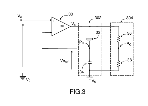
Figure 3 illustrates a hybrid control device according to one embodiment
of the invention, combining both charge and voltage control modes.
The device (300) combines a first circuit (302) for controlling the charge
control mode with a second circuit (304) for controlling the voltage control
mode,
the two circuits being coupled to an operational amplifier (30).
Advantageously, the hybrid setup of the invention makes it possible to
switch between both charge and voltage modes automatically.
The amplifier (30) receives an input voltage Ve on a first, non-inverting
(+) input and delivers, as output 'OUT', an output voltage Vs.
The first circuit (302) comprises a piezoelectric actuator (32) and a
capacitor (34) in series. The piezoelectric actuator (32) is connected to the
output
'OUT' and to the inverting input of the operational amplifier (30). The
capacitor
CA 02989250 2017-12-12
(34) in series is connected to the inverting input of the operational
amplifier and
to a low voltage Vo.
The first circuit is a capacitive circuit comprising a piezoelectric actuator
and a capacitor in series, said capacitive circuit being connected by the free
end
5 of the piezoelectric actuator to the output of the operational amplifier
and by the
free end of the capacitor to a low-voltage terminal.
The second circuit (304) comprises discrete components in series, and is
composed of a first resistor (36) and of a second resistor (38) in series. The
first
resistor (36) is connected to the output 'OUT' and to the inverting input of
the
10 operational amplifier (30). The second resistor (38) is connected to the
inverting
input of the operational amplifier and to a low voltage Vo.
The second circuit is a resistive circuit comprising a first resistor and a
second resistor in series, said resistive circuit being connected by the free
end of
the first resistor to the output of the operational amplifier and by the
second
resistor to a low-voltage terminal.
The low voltage may, preferably, be brought to ground.
The inverting output (-) of the amplifier (30) corresponds to a common
connection point `13,' between the two, capacitive (302) and resistive (304),
circuits. The common connection point Pc is shared between the actuator (32)
and
the capacitor (34), respectively, for the first circuit (302), and between the
first
resistor (36) and the second resistor (38), respectively, for the second
circuit
(304). The common connection point 'Pc' has a voltage denoted by 'Vcre?.
Thus, the device is characterized in that the inverting input of the
operational amplifier is both connected to the common ends of the
piezoelectric
actuator and of the capacitor, and is connected to the common ends between the
first and the second resistor, the capacitive circuit and the resistive
circuit
forming an impedance bridge.
CA 02989250 2017-12-12
11
The device of the invention therefore provides an impedance bridge
formed by the capacitors (32, 34) of the first circuit (302) and by the first
and
second resistors (36, 38) of the second circuit (304).
Equilibrium of this bridge is achieved when:
Rref
pzi
Cref
RPzi (10) where
- Cpzt represents the intrinsic capacitance of the piezoelectric actuator
(32);
- Cref represents the capacitance of the capacitor (34);
- Rpzt and Rref represent the first and second resistances, respectively, of
the second circuit (304).
Advantageously, the values of the resistances of the resistive bridge (304)
are defined so as to compensate for several effects:
- a choice of high resistance values leads to a decrease in the
bandwidth
of the setup, and vice versa;
- on choosing low resistance values, the frequency of the control signal
must be high in order to allow charge control;
- a choice of high values for the resistances Rpzt and Rref, of the
order of
MS) to GD, has the drawback that the discrete resistances have the
same order of magnitude as the values of the leakage resistances of the
capacitors, which does flot allow the level of optimization given by the
Rpzi =Cref
equation R
ref Pzito be reached and does flot allow a hybrid
control
that decreases the hysteresis of the actuators to be obtained.
In the Laplace domain, the output voltage Vs(p) of the amplifier and the
voltage at the terminais of the piezoelectric actuator Vpzt(p) are expressed
by the
following equations (11) and (12), respectively:
CA 02989250 2017-12-12
12
1+ Rcrej* R _____________________ Pz` (Cc õf +C pz,)P
Rc rej +Rpzt * Rc rej + R pz,
Vs(p)=- *Ve(P)
Rc 1+ RpzI* Cpz1
rej (11)
pzl + (R pz,* Cc õf)p
Rcref
(12)
where the parameters represent:
- 'p' is the Laplace variable;
- 'Cpzt' is the intrin sic capacitance of the piezoelectric actuator;
- 'Rpzt' is the resistance in parallel with the actuator;
- 'Ccref is the capacitance of the reference capacitor;
- 'Rcref is the resistance in parallel with the reference capacitor.
The value of the chopping frequency of the device of figure 3 may be
determined according to the maximum output current ismax delivered by the
operational amplifier, the amplitude A, of the input voltage Ve(t), which is
considered to be sinusoidal, and the value of the capacitance of the reference
capacitor Cref, according to the following equation:
max
f 2*Ir* Ae*Ccref (13)
In considering equation (12), those skilled in the art observe that, for a
given input voltage, when 'p' tends toward 0, the gain of the transfer
function
tends toward 'Rpzt/Rcre?, and, when 'p' tends toward infinity, the gain of the
transfer function tends toward 'Ccref/Cpzt'.
From a physical standpoint, when the frequency tends toward 0, the
capacitors Cpzt (32) and Cref (34) are equivalent to open circuits. The output
current flows solely through the resistors Rpzt (36) and 'Rcre? (38). In this
mode,
the device behaves like a voltage control circuit.
CA 02989250 2017-12-12
13
When the frequency tends toward infinity, the capacitors Cpzt (32) and Cref
(34) are equivalent to short circuits. Ail of the output current flows through
these
two capacitors. In this mode, the device behaves like a charge control
circuit.
Advantageously, at extreme low and high frequencies, there is no phase
shift between the input and output signais. The low-frequency gain is set by
the
resistors (36, 38) while, at high frequencies, it is set by the capacitors
(32, 34).
The output current is given by the following equation:
(1)¨ (t)
dt Rc ref (14)
The time constant of the setup is:
t = Rpzt *Cpzt (15)
For switching between the charge and voltage control modes to take place
automatically, the voltage gains at high and low frequency must be equal.
When this condition of equality of voltage gains is met, the behavior of
the device of the invention is as follows:
After the application of a control signal at a given frequency, the
piezoelectric actuator is displaced to a certain position, with decreased
hysteresis.
It is the charge control mode with the capacitive portion of the first circuit
(302),
composed of Gd- and Cpzt, that is brought into play.
Next, in the steady state, with the application of a continuous signal, the
resistive portion of the second circuit (304), composed of Rpt and Rrer, comes
into operation. This is the voltage control mode.
Since the voltage and charge control gains are identical, the voltage at the
terminais of the piezoelectric actuator (32) is constant.
CA 02989250 2017-12-12
14
Thus, advantageously, the actuator is no longer displaced, the
displacement being held stable. There is therefore no longer any creep, unlike
the
known charge control devices.
The control of piezoelectric actuators for Fabry-Pérot interferometers
must observe precise positioning requirements. Specifically, these
piezoelectric
actuators must ensure the displacement and alignment of the flats of the
interferometer for a travel of 0-200 iim with a positioning accuracy of the
order
of a nanometer, a very high degree of reproducibility of positioning (very low
hysteresis) and a linearity error, along with very low drift (very low creep).
The
device of the present invention allows these requirements to be met.
Figure 4 illustrates an exemplary implementation of the device of the
invention when applied to the control of movable mirrors in Fabry-Pérot
interferometers.
The hybrid control device such as detailed in figure 3 is shown in figure 4
with the references (40) for the operational amplifier, (42) for the
piezoelectric
actuator Cp,t, (44) for the reference capacitor Cõf and (46) and (48) for the
first
and second resistors, respectively.
Various electronic components, applied conventionally for those skilled in
the art, are added around the device of the invention in order to allow the
desired
operating behavior. Thus, in a non-limiting manner, capacitors (Cl, C2, C3,
C4)
may be added in order to allow the supply voltages (+Vcc, -Vcc) to be
decoupled,
and unidirectional transil diodes (Dl, D2) for limiting the voltage at the
terminals
of the piezoelectric actuator (42). A resistor Rhm may be added in order to
limit
the current drawn by the actuator, along with a phase compensation capacitor
Cunp. Diodes (D3, D4) for protecting the differential input of the amplifier
(40)
may be added, along with transil diodes (D5, D6) for protecting the setup from
overvoltages and polarity reversais of the supply voltages.
In one preferred implementation, the amplifier may be a high-voltage
amplifier supplied with between -60 V and +160 V, the voltage at the terminais
CA 02989250 2017-12-12
of the actuator may be limited to +150 V and -20 V, respectively, and the
current
drawn by the actuator may be limited to 130 mA.
The table below shows the results of comparing the hysteresis curves
obtained with an operational amplifier of gain 20 controlling multiple
5 piezoelectric actuators by conventional voltage control and by hybrid
control
according to the device of the present invention.
The piezoelectric actuators used have the following properties:
Parameter Value Unit
Supply voltage (Vpe) -20 to +150 V
Max. displacement without load (ADpe) 344
Intrinsic capacitance Cpzt 10
Free-free resonant frequency 2738 Hz
(Frpe)
Free-blocked resonant frequency 634 Hz
(Frpzt)
Free-free response time (tripe) 0.18 ms
Free-blocked response time (tripe) 0.79 ms
Resolution 3.44 nm
Mass (Mpe) 47.5 g
Stiffness (Kpe) 0.55 N/Ftm
B locking force 189
Temperature variation index (kt) 3.38 tm/ K
Hysteresis (H) 16 <H <20 %
CA 02989250 2017-12-12
16
Drift factor Not specified
The comparison in the table below is given for measurements taken on
three piezoelectric actuators.
Actuator Voltage control Hybrid amplifier Decrease factor
hysteresis hysteresis
1 19.01% 0.76% 96.00%
2 19.42% - 0.85% 95.62%
3 16.82% 0.23% 98.63%
In the last column, a substantial decrease in the hysteresis regardless of
the actuator may be observed. Specifically, the voltage controls (2n1 column)
result in a hysteresis of the order of 20% of the total amplitude of
displacement of
the piezoelectric actuators while for the hybrid amplifier (3rd column) this
same
hysteresis is decreased to about 1%.
Figure 5 illustrates one variant implementation of the device of the
invention in the context of unipolar control.
The hybrid control device such as detailed in figure 3 is shown in figure 5
with the references (50) for the operational amplifier, (52) for the
piezoelectric
actuator Cpe, (54) for the reference capacitor Cref and (56) and (58) for the
first
and second resistors, respectively. In this setup, one terminal of the
actuator (52)
is linked to ground, the other terminal participating in the midpoint of the
impedance bridge.
Various electronic components, applied conventionally for those skilled in
the art, are added around the device of the invention in order to allow the
desired
operating behavior. Thus, in a non-limiting manner, unidirectional transil
diodes
(D3, D4) may be added in order to limit the voltage at the terminals of the
piezoelectric actuator (52).
CA 02989250 2017-12-12
17
In the setup of figure 5, an instrumentation amplifier (510) is added, for
the purpose of equalizing the reference voltage and the voltage across the
terminais of the set (Rref, Cred. One input of the instrumentation amplifier
receives the output of the operational amplifier, the other input of the
instrumentation amplifier being connected to the midpoint of the impedance
bridge. The output of the instrumentation amplifier is looped back to the
inverting
input of the operational amplifier.
Rpziref
By statingP:1* C = * C R C
pzi ref ref
i.e.fel Pzi this setup
makes it
possible to produce an ideal low-frequency charge amplifier.
Since the operation of the hybrid amplifier is the combination of two
(voltage and charge) control modes, it is important to identify the frequency
range within which each operating mode is dominant. This frequency range is
-= 1
characterized by the center frequency defined by the equation: 2 71 R2, C,
For frequencies higher than fc, it is then the charge control mode that is
brought into play and, for frequencies lower thanfc, it is the voltage control
mode
that dominates.
Such a setup is particularly suitable for the unipolar control of
piezoelectric actuators, the control of which does not require high voltages,
of the
order of 10 V.
Figure 6 illustrates one variant implementation of the device of the
invention in the context of unipolar control for the cases in which the
control
voltage is high, such as in the case of large displacements. For the sake of
simplicity, the set of components of the variant of figure 4 is referenced
solely by
(400) and they are flot described again. In this variant, a non-inverting
amplifier
(60) is added upstream of the hybrid amplifier.
CA 02989250 2017-12-12
18
In this setup, the first amplifier (60) is used to amplify the control signal
V1n. The gain of this amplifier is then given by the relationship: R8
The second portion of the setup consists of the hybrid amplifier (400)
having one of the terminals of the actuator connected to ground.
Rp z _Crej
In such a setup, the equation Rref C is conserved, making it possible
to obtain the same decrease in hysteresis as in the setup of figure 4.
Advantageous applications of this setup are adaptive optics applications for
the
open-loop control of deformable mirrors.
The present description thus illustrates various non-limiting
implementations of the invention. The examples have been chosen so as to allow
a good understanding of the principles of the invention, but these are in no
way
exhaustive, and should allow those skilled in the art to provide modifications
and
implementation variants while keeping the same principles.
It has been shown that the hybrid amplifier of the invention allows the
amplitude of the hysteresis of the piezoelectric actuators to be significantly
decreased. The proposed device thus makes it possible to linearize the
displacement of an actuator according to the voltage applied to its terminals
or to
the setpoint voltage.
Another advantage of the device of the invention is that it does not require
a hysteresis model (Preisach, Maxwell, etc.) and may consequently operate with
any piezoelectric actuator, within the limits of the electronic setup. The
only
parameters that must be known for the implementation thereof are the intrinsic
capacitance of the piezoelectric actuator at rest and its bandwidth, such data
generally being available in the catalogs of piezoelectric actuator
manufacturers.
CA 02989250 2017-12-12
19
The fields of application of the hybrid amplifier of the invention could be,
for example, nano- and micropositioning, mechatronics applications or even the
field of virtual reality.